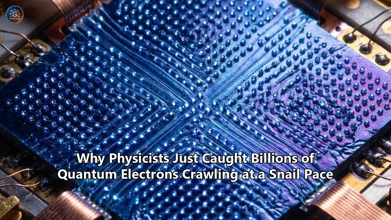
Inside a laboratory at the University of Chicago’s Pritzker School of Molecular Engineering, an ultraviolet laser focused to a ten-micrometer beam struck the cleaved surface of a layered iron-germanium-tellurium crystal. When the instrument detected the particles knocked free by the light, the velocity readouts confounded standard solid-state expectations: billions of electrons, typically accustomed to zipping through conductive lattices at speeds approaching thousands of kilometers per second, had slowed to a near-total crawl.
The experimental results, published in Science Advances by a research team led by Assistant Professor Shuolong Yang alongside postdoctoral scholars Gabriele Berruto and Qiang Gao, document an exotic electronic state inside the van der Waals ferromagnet $\text{Fe}_5\text{GeTe}_2$. In this material, huge populations of electrons surrender their individual kinetic energy to form a dispersionless "flat band" directly at the Fermi level, where their group velocity drops toward zero.
Unlike conventional insulators or disordered systems where electrons grind to a halt because they run into atomic impurities or structural defects, these particles decelerate while locked in collective, macroscopic quantum coherence. They behave not as isolated charges ricocheting through atomic corridors, but as a synchronized fluid moving across the crystal in lockstep.
Standard Metal Band Structure            Flat-Band System (Fe5GeTe2)
      Energy (E)                               Energy (E)
          |     /                                  |
          |    /  Steep dispersion                 |         Fermi Level (Ef)
   Ef ----+---/--- (High velocity)          Ef ----+========= (Velocity ≈ 0)
          |  /   vg = (1/ħ)(dE/dk)                 |         Collective Coherence
          | /                                      |
          +------------ Momentum (k)               +------------ Momentum (k)
The discovery upends theoretical models governing how magnetic order and charge transport interact in low-dimensional materials. More importantly, it thrusts $\text{Fe}_5\text{GeTe}_2$ into the center of a high-stakes scientific contest. For years, physicists have pursued distinct, competing architectures to halt electrons: twisting sheets of graphene to exact nanoscale angles, engineering frustrated geometric lattices like Japanese basket-weave kagome patterns, or leaning on heavy-fermion intermetallics.
The Chicago team’s realization relies on an entirely different mechanism: an intrinsic, electronic-interaction-driven flat band coupled to a real-space charge order that persists at temperatures far higher than its competitors. The result could reshape the engineering of next-generation magnetic memory and ultra-low-power computing devices.
The Physics of Sluggishness: Dispersion, Effective Mass, and the Flat Band
To understand why physicists find crawling electrons so significant, one must look at how momentum relates to kinetic energy inside a crystalline lattice. In classical mechanics, an object’s velocity tracks linearly with its momentum, scaled by its invariant mass. In the quantum architecture of a solid, however, an electron moves through a periodic potential established by a grid of atomic nuclei. Its energy states coalesce into electronic bands, mapped as an energy-momentum dispersion relation, $E(\mathbf{k})$, where $\mathbf{k}$ denotes the crystal momentum vector.
The group velocity $v_g$ of an electron wavepacket through the crystal lattice is given by the gradient of this dispersion relation in momentum space:
$$v_g(\mathbf{k}) = \frac{1}{\hbar} \nabla_{\mathbf{k}} E(\mathbf{k})$$
In standard conductors such as copper, aluminum, or gold, the energy bands cut sharply across the Fermi energy ($E_F$). The slope $\nabla_{\mathbf{k}} E(\mathbf{k})$ is steep, giving electrons high velocities—typically between $10^5$ and $10^6$ meters per second. These electrons race through the lattice, colliding periodically with vibrating atoms (phonons) or structural flaws, which manifests macroscopically as electrical resistance.
+-----------------------------------------------------------------------------------+
| Dispersion Steepness vs. Velocity Analogy                                         |
|                                                                                   |
| Steep Slope (Standard Conductor)           Flat Slope (Fe5GeTe2 Flat Band)        |
| Water racing down a vertical waterfall     Water pooled on a flat, level plane    |
| -> Maximum kinetic energy                  -> Kinetic energy vanishes             |
| -> Independent, high-speed transit         -> Coulomb repulsion forces lockstep   |
+-----------------------------------------------------------------------------------+
When an electronic band flattens out, the derivative $\nabla_{\mathbf{k}} E(\mathbf{k})$ approaches zero across a significant portion of the Brillouin zone. As the slope vanishes, the group velocity drops to near zero. Yang illustrates the dynamic by comparing it to fluid dynamics: "Water flowing down a steep waterfall moves at extreme speed. But if you flatten the terrain, the water slows to an absolute crawl. That is what happened to these electrons. Their kinetic energy has been extinguished".
Simultaneously, the effective mass $m^$ of the electron quasiparticle, which is inversely proportional to the curvature of the energy band, surges toward infinity:
$$m^ = \hbar^2 \left( \frac{\partial^2 E}{\partial k^2} \right)^{-1} \to \infty$$
When an electron’s effective mass becomes massive and its kinetic energy drops to zero, the physics changes entirely. In ordinary metals, kinetic energy dominates over the Coulomb repulsion between electrons; the particles have enough momentum to bypass one another, behaving essentially as independent, free-moving entities under Landau's Fermi liquid theory.
When the kinetic bandwidth $W$ contracts until it is dwarfed by the on-site Coulomb repulsion energy $U$ ($U/W \gg 1$), the electrons can no longer ignore each other. They must coordinate their movements to minimize their shared electrostatic repulsion.
In most materials, pushing a system into a regime of strong Coulomb correlation simply causes the electrons to lock into a localized Mott insulating state or scatter incoherently, creating an impenetrable quantum traffic jam where charge conduction collapses entirely. The anomalous feature of the University of Chicago discovery is that the electrons in $\text{Fe}_5\text{GeTe}_2$ do not scatter into an incoherent mess.
"We’re not measuring one electron," Yang explained. "We’re measuring the interaction of thousands or millions of electrons, and they are all moving together in a coherent way. That's a quantum many-body phenomenon, and it's actually a very weird thing". The charges remain mobile enough to conduct, but they do so in synchronized lockstep, preserving their collective phase relationships while moving at a snail's pace.
Four Pathways to Freezing Electrons: A Comparative Architecture
The discovery in Chicago does not exist in an academic vacuum. Halting electrons without destroying their quantum coherence has become a focal point of modern condensed matter physics. Scientists have pursued several competing technological and material approaches to engineer flat bands and study correlated phenomena. Each route features starkly different mechanisms, manufacturing constraints, operating temperatures, and operational tradeoffs.
COMPETING FLAT-BAND ARCHITECTURES

1. Moiré Superlattices (Twistronics)
   [ Graphene Sheet 1 ]
         \ (θ ≈ 1.1°)
   [ Graphene Sheet 2 ]
   * Mechanism: Long-wavelength spatial interference pattern
   * Tradeoff: Extreme fabrication fragility; operates below 2 Kelvin

2. Geometrically Frustrated Lattices (Kagome / Pyrochlore)
   * Mechanism: Destructive quantum interference via corner-sharing triangles/tetrahedra
   * Tradeoff: Hardcoded by crystal symmetry; flat bands often lie far from Fermi energy

3. Kondo Heavy-Fermion Systems
   * Mechanism: Hybridization of localized f-electrons with itinerant conduction states
   * Tradeoff: Heavy reliance on radioactive or rare elements; cryogenic operating limits

4. Interaction-Driven van der Waals Systems (Fe5GeTe2)
   * Mechanism: Intrinsic many-body Coulomb interactions driving charge ordering
   * Tradeoff: Complex stoichiometry; stable at 100 Kelvin with room-temperature magnetism
Pathway 1: Moiré Superlattices and Nanoscale Twistronics
The most famous approach to flat bands over the past decade is twistronics, pioneered theoretically by Allan MacDonald and Rafi Bistritzer and demonstrated experimentally by Pablo Jarillo-Herrero’s group at the Massachusetts Institute of Technology in 2018.
Twistronics achieves flat bands through physical geometry. By stacking two atomically thin sheets of graphene and twisting one relative to the other by a precise "magic angle" of approximately 1.1 degrees, researchers produce a moiré superlattice—a long-period interference pattern that stretches hundreds of times the diameter of a single carbon hexagon.
Twisted Bilayer Graphene (Moiré Superlattice)
Top Layer:    o---o---o---o---o
             /   /   /   /   /
Bottom Layer:  o---o---o---o---o   (Rotated by θ = 1.1°)
Result: Long-period supercell quenches kinetic energy into flat bands
This massive supercell radically downscales the size of the Brillouin zone. The original, steeply dispersing Dirac cones of graphene are folded repeatedly into a much smaller mini-Brillouin zone. At the magic angle, interlayer tunneling hybridizes the electron states, flattening the dispersion bands near zero energy and quenching the electrons' Fermi velocity.
The Tradeoffs of Twistronics
- Fabrication Bottlenecks: Fabricating magic-angle twisted bilayer graphene (MATBG) or twisted transition metal dichalcogenides (TMDs) requires meticulous nanofabrication. Stacking two-dimensional layers with an angular precision of $\pm 0.05^\circ$ demands specialized polymer-stamp transfer setups inside inert-gas gloveboxes.
- Structural Instability: Twisted flakes suffer from spatial inhomogeneity and strain relaxation. Over time or across larger device areas, the twist angle drifts, washing out the flat-band condition across the device.
- Cryogenic Dependency: While moiré flat bands have yielded unconventional superconductivity, orbital magnetism, and correlated insulating states, these phenomena typically vanish at temperatures above 1 to 3 Kelvin. Maintaining the flat-band state requires liquid helium or dilution refrigerators, confining twistronics largely to academic laboratories.
Pathway 2: Geometrically Frustrated Lattices (Kagome and Pyrochlore Crystals)
A separate camp of physicists, including teams led by Joseph Checkelsky, Riccardo Comin, and Mingda Li at MIT, has focused on stoichiometric, single-crystal compounds whose atomic structures naturally cancel electron motion through destructive quantum interference.
Rather than relying on mechanical twisting, these researchers grow crystals featuring kagome lattices—arrangements of corner-sharing triangles—or their three-dimensional analogues, pyrochlore lattices.
Kagome Geometry (Corner-Sharing Triangles)
        /\          /\
       /  \        /  \
      /____\______/____\
      \    /      \    /
       \  /        \  /
        \/__________\/
Trapped Orbit: Electron waves hopping clockwise and counter-clockwise
interfere destructively, pinning the particle inside the hexagonal void.
When an electron travels through a kagome lattice, its quantum wavepacket can hop around the perimeter of the corner-sharing triangles. If the geometry is structured correctly, the quantum paths traversing clockwise and counterclockwise acquire a phase difference of exactly $\pi$ radians ($180^\circ$).
The two paths interfere destructively, canceling the probability amplitude for the electron to hop out of the unit cell. The particle becomes trapped inside the real-space hexagonal void of the lattice, yielding a completely flat electronic band in momentum space without any artificial twisting.
In late 2023, Checkelsky's group extended this concept into three dimensions by synthesizing crystals of the pyrochlore metal $\text{CaNi}_2$, where corner-sharing nickel tetrahedra cage electrons in all spatial directions.
The Tradeoffs of Frustrated Lattices
- Energetic Misalignment: While frustrated lattices naturally host flat bands, those bands rarely land precisely at the Fermi level ($E_F$). In materials like $\text{CoSn}$ or $\text{FeSn}$, the geometrically trapped flat bands often sit hundreds of millielectronvolts above or below the energy window where conduction electrons operate. If the flat band is buried deep below the Fermi surface, it has little influence on the material's conduction properties.
- Static Chemical Architecture: The electronic structure is fixed by the crystal’s thermodynamic synthesis. Shifting the flat band to the Fermi level requires aggressive chemical doping, which often introduces atomic defects that disrupt the subtle destructive interference keeping the band flat in the first place.
Pathway 3: The Kondo Engine and Heavy-Fermion Systems
A third route to halting electrons involves heavy-fermion materials, a domain long analyzed by condensed matter theorists like Qimiao Si at Rice University. First discovered in the 1970s in intermetallic compounds containing rare-earth or actinide elements (such as $\text{CeCu}_6$, $\text{CeCoIn}_5$, or $\text{UPt}_3$), these systems generate slow-moving electrons through the Kondo resonance.
Kondo Lattice Hybridization
Itinerant Conduction Electrons (Broad s/p/d band)
                    ||
                    || Hybridization (below Kondo Temperature Tk)
                    \/
Localized Magnetic Moments (Unfilled, localized 4f or 5f orbitals)
                    ||
                    \/
Extremely Heavy Quasiparticles (m* ≈ 100 to 1000 m_e)
In a Kondo lattice, itinerant conduction electrons (typically from broad $s$, $p$, or $d$ atomic orbitals) interact with an array of localized magnetic moments residing in tightly bound $4f$ or $5f$ atomic shells. Above a characteristic Kondo temperature ($T_K$), these two electron populations remain separate.
As the material cools below $T_K$, the conduction electrons begin screening the localized magnetic moments, entangling their spins. This quantum many-body hybridization creates a narrow, sharp resonance at the Fermi level.
Quasiparticles emerging from this hybridization inherit characteristics of the localized $f$-orbitals, developing an effective mass hundreds or even thousands of times greater than that of a bare electron. These massive quasiparticles crawl through the crystal lattice, enabling studies of quantum criticality, non-Fermi liquids, and unconventional superconductivity.
The Tradeoffs of Heavy Fermions
- Exotic Elements and Toxicity: Heavy-fermion materials rely on lanthanide or actinide elements like cerium, ytterbium, uranium, or plutonium, which present synthesis difficulties, chemical toxicity, and oxidation issues.
- Extreme Cryogenics: The characteristic Kondo temperatures governing these interactions are low, typically ranging from a few Kelvin down to millikelvin levels. Coherence dissolves rapidly as thermal vibrations wash out the delicate spin-screening resonance.
Pathway 4: The Chicago Paradigm: Interaction-Driven Flat Bands in $\text{Fe}_5\text{GeTe}_2$
The breakthrough achieved by Shuolong Yang’s team at the University of Chicago bypasses the constraints of the first three approaches. They did not construct a moiré superlattice by twisting individual atomic sheets, nor did they use geometric frustration or rare-earth $f$-orbitals.
Instead, they demonstrated that an intrinsic, interaction-driven flat band can emerge spontaneously at the Fermi level within an iron-based van der Waals crystal: $\text{Fe}_5\text{GeTe}_2$.
Fe5GeTe2 Layered Architecture
[Te - Ge - Fe - Fe - Fe - Ge - Te]  <-- Covalently bonded atomic slab
----------------------------------  <-- Van der Waals Gap (weakly bonded)
[Te - Ge - Fe - Fe - Fe - Ge - Te]  <-- Covalently bonded atomic slab
* Features iron occupancy vacancies and intrinsic ferromagnetism
* Electrons slow down via spontaneous electronic correlation and charge ordering
$\text{Fe}_5\text{GeTe}_2$ is a layered van der Waals ferromagnet. Discovered in 2019, it gained quick attention because its magnetic ordering survives at unusually high temperatures—reaching roughly 260 to 310 Kelvin in bulk form, and exceeding 300 Kelvin in exfoliated or iron-intercalated thin films.
The crystal structure consists of slabs of iron ($\text{Fe}$) and germanium ($\text{Ge}$) atoms sandwiched between outer layers of tellurium ($\text{Te}$). These slabs are held together across a van der Waals gap by weak dispersion forces, allowing the material to be thinned down to single 2D layers.
What makes $\text{Fe}_5\text{GeTe}_2$ chemically complex is the internal arrangement of its iron atoms. The lattice contains three distinct crystallographic iron sites: $\text{Fe}(1)$, $\text{Fe}(2)$, and $\text{Fe}(3)$. The $\text{Fe}(1)$ site sits close to the tellurium boundary and is split between two positions above and below the germanium plane, exhibiting partial, disordered occupancy.
Physicists had assumed this disorder simply degraded electronic coherence. Standard density functional theory (DFT) calculations treated $\text{Fe}_5\text{GeTe}_2$ as an itinerant ferromagnet with broad, dispersive $d$-electron bands crossing the Fermi level at high speed.
+-----------------------------------------------------------------------------------+
| Why Fe5GeTe2 Surprised Theorists                                                  |
|                                                                                   |
| Theoretical Prediction (DFT):             Experimental Reality (Laser-ARPES):     |
| * Disordered iron occupancy               * Highly coherent quantum state         |
| * Itinerant, high-velocity d-electrons    * Ultra-flat band pinned at Fermi level |
| * Incoherent scattering from defects      * Electrons move slowly in lockstep     |
| * Simple band ferromagnetism              * Spontaneous √3 × √3 R30° charge order |
+-----------------------------------------------------------------------------------+
Using high-resolution, micro-focused angle-resolved photoemission spectroscopy (micro-ARPES), Yang and his colleagues found that theoretical models had missed the mark. The $d$-electrons within the iron layers interact through strong Coulomb repulsion, spontaneously splitting the energy bands and generating an ultra-flat electronic band directly pinned at the Fermi energy.
Simultaneously, the flat band triggers a real-space charge density wave: a $\sqrt{3} \times \sqrt{3}\, R30^\circ$ charge order manifested by distinct band folding within 30 millielectronvolts of the Fermi surface.
The electrons in this material slow down not because an experimentalist twisted the crystal, nor because the atomic lattice forced destructive interference, but because strong internal electron-electron interactions prompted them to reorganize into an ordered state.
This correlation quenches their velocity while maintaining quantum coherence. The spectral weight of this flat band exhibits a logarithmic temperature dependence reminiscent of a heavy Fermi liquid, confirming that the slow electrons behave as coherent quasiparticles rather than trapped, immobile charges.
Detailed Tradeoff Matrix: Comparing Approaches
To see where the Chicago discovery fits within modern physics, we can compare the four major architectures along five primary axes: operating temperature limits, fabrication complexity, band tuning, susceptibility to structural disorder, and scalability for device integration.
| Parameter | Moiré Superlattices (Twistronics) | Geometrically Frustrated Lattices (Kagome/Pyrochlore) | Heavy-Fermion Systems (Kondo Lattices) | Interaction-Driven vdW Systems ($\text{Fe}_5\text{GeTe}_2$) |
|---|---|---|---|---|
| Primary Mechanism | Long-period spatial interference from physical rotation ($\theta \approx 1.1^\circ$). | Destructive quantum interference of hopping paths on corner-sharing vertices. | Hybridization between itinerant conduction bands and localized $f$-orbitals. | Strong Coulomb correlation driving spontaneous charge order and band flattening. |
| Operating Temperature | Cryogenic: Typically $0.05\text{ K} - 4\text{ K}$. | High stability: Geometric properties survive above $300\text{ K}$, though correlations often require $<50\text{ K}$. | Cryogenic: Typically $0.1\text{ K} - 20\text{ K}$ ($T_K$ rarely exceeds $50\text{ K}$). | Elevated Coherence: Flat band and charge order survive up to $100\text{ K}$; magnetism persists past $300\text{ K}$. |
| Band Position Control | Electrostatic gating shifts $E_F$ across the flat band without chemical alterations. | Rigid: Flat bands often sit far from $E_F$; requires chemical doping that can degrade crystal quality. | Rigid: Band is anchored to $E_F$ by hybridization, but difficult to shift with external electrostatic gates. | Dynamically Switchable: Pinning occurs intrinsically at $E_F$; accessible to optical laser switching. |
| Fabrication Difficulty | Extreme: Requires nanometer-scale alignment, micro-stamping, and sub-$0.1^\circ$ angle precision. | Moderate: Bulk single crystals or thin films grown via chemical vapor transport (CVT) or MBE. | Moderate to High: Requires arc-melting or flux growth of reactive, radioactive, or rare elements. | Straightforward: Grown as bulk single crystals or exfoliated using standard 2D tape techniques. |
| Disorder Tolerance | Highly sensitive: Slight angular variations or strain gradients disrupt the moiré state. | Moderate: Atomic defects interrupt destructive interference loops, turning flat bands dispersive. | High: Kondo screening can survive moderate chemical disorder in the conduction band. | Uniquely Robust: Flat band emerges in spite of intrinsic iron vacancy disorder in the lattice. |
Mechanical Twisting versus Spontaneous Ordering
When contrasting twistronics with the University of Chicago's interaction-driven van der Waals system, the trade-off between fabrication precision and functional reliability becomes clear.
In magic-angle graphene, the experimentalist must manually impose a synthetic periodicity on non-interacting sheets of carbon. If the twist angle slips by just $0.1^\circ$ during thermal cycling or gate biasing, the superlattice changes and the flat band dissolves.
In $\text{Fe}_5\text{GeTe}_2$, the flat band requires no mechanical intervention. The electrons organize themselves into an interaction-driven flat band via internal Coulomb interactions.
This internal organization explains why the Chicago team observed coherent flat-band dynamics at 100 Kelvin—a temperature range roughly fifty times warmer than that required for correlated states in magic-angle twisted bilayer graphene.
Understanding these differences is critical because manipulating quantum electron behavior in scalable technologies requires devices that can operate without liquid helium infrastructure.
THERMAL CEILINGS COMPARED

Twistronics (Graphene):
[ 1.7 K ] Superconductivity vanishes
|
Heavy Fermions (CeCoIn5):
[ 2.3 K ] Coherent heavy state collapses
|
Interaction-Driven Flat Band (Fe5GeTe2):
[================================================== 100 K ] Coherent slow-motion flat band persists
|
Bulk Magnetism (Fe5GeTe2):
[================================================================================ 310 K ] Room-temperature ferromagnetism
Structural Traps versus Electronic Self-Organization
The contrast between geometrically frustrated lattices (kagome and pyrochlore) and $\text{Fe}_5\text{GeTe}_2$ is just as sharp. In a kagome metal such as $\text{CoSn}$ or a pyrochlore like $\text{CaNi}_2$, the flat band is an invariant consequence of single-particle hopping physics.
The destructive interference occurs whether electrons interact strongly or not; it is hardwired into the crystal’s spatial symmetries.
The primary drawback is lack of control. Because the band is a product of fixed atomic coordinates, it rarely coincides with the Fermi level. If a flat band sits 500 millielectronvolts beneath the Fermi energy, its trapped electrons are entirely filled and cannot carry electrical current or influence the material's conduction properties.
The material acts like a conventional conductor governed by other, more dispersive bands that happen to cross the Fermi surface.
In $\text{Fe}_5\text{GeTe}_2$, the flat band does not rely on geometric caging. Its position is pinned directly at the Fermi level precisely because it is generated by electronic correlations. When electrons interact strongly through Coulomb forces, the energetic penalties of occupancy redistribute charge states near the Fermi surface, naturally aligning the flat band with the conduction threshold.
The resulting charge order ($\sqrt{3} \times \sqrt{3}\, R30^\circ$) folds the electronic bands, stabilizing the flat-band manifold within 30 millielectronvolts of the chemical potential.
Consequently, the electrons crawling at a snail's pace are the active charge carriers driving conduction, rather than inert background states.
Laser ARPES: The Spectroscopic Smoking Gun
Confirming that billions of electrons are moving coherently at low speeds within a solid requires advanced experimental diagnostics. The Chicago team proved the existence of this interaction-driven flat band using high-resolution, micro-focused Angle-Resolved Photoemission Spectroscopy (micro-ARPES).
Laser-ARPES Measurement Scheme

  [ Ultrafast UV Laser ] (hν = 6.0 eV)
            |
            | (Focused to 10 µm spot)
            v
   /=================\
  |  Fe5GeTe2 Sample  |  --> Ejected Photoelectrons
   \=================/           |
                                 v
                     [ Hemispherical Analyzer ]
                                 |
                                 v
         Maps Kinetic Energy (E_kin) vs. Emission Angle (θ)
                                 |
                                 v
         Extracts Band Dispersion E(k) and Group Velocity v_g
ARPES leverages the photoelectric effect originally explained by Albert Einstein. A high-energy photon strikes the crystal surface, transferring its energy to an electron within the material. If this energy exceeds the material's work function $\Phi$, the electron is ejected into the vacuum.
By measuring the kinetic energy ($E_{kin}$) and the emission angle ($\theta, \phi$) of these escaping photoelectrons, researchers use the conservation laws of energy and momentum to map the electron’s original band structure inside the crystal:
$$E_B = h\nu - \Phi - E_{kin}$$
$$\mathbf{k}_{\parallel} = \frac{1}{\hbar} \sqrt{2m_e E_{kin}} \sin\theta$$
For $\text{Fe}_5\text{GeTe}_2$, capturing accurate spectra had challenged researchers for years because the material naturally forms microscopic domains with varying surface terminations and iron concentrations. If an ARPES measurement averages over a millimeter-wide photon beam, these distinct domains blur together. The resulting spectra display smeared, indistinct bands, which led early studies to misinterpret the material's electronic structure as merely disordered and incoherent.
The University of Chicago team resolved this issue by focusing an ultraviolet laser beam ($h\nu = 6.0\text{ eV}$) down to a spot just 10 micrometers across. This tight spatial focus allowed them to probe single, atomically pristine crystalline domains.
Spectral Profile Across the Brillouin Zone

     Energy Relative to Ef (meV)
          0 -----------------------------------  Flat Band (dE/dk ≈ 0)
        -10
        -20
        -30 ===================================  Charge-Order Band Folding
        -40
        -50
           \                 |                 /
            \                |                /  Underlying Dispersive Bands
             \               |               /
              Γ              K               M   Momentum Space Points
The micro-ARPES measurements revealed three primary spectroscopic signatures:
- A Dispersionless Horizon: Rather than displaying parabolically dispersing bands cutting across $E_F$, the emission intensity showed a flat horizontal band spanning the Brillouin zone. Over a broad momentum range, the variation in energy was negligible ($\Delta E < 5\text{ meV}$), confirming that group velocity $v_g$ dropped to near zero.
- Charge-Order Band Folding: The researchers identified replica bands folded back toward the center of the Brillouin zone within 30 millielectronvolts below the Fermi level. This band folding confirmed the formation of a $\sqrt{3} \times \sqrt{3}\, R30^\circ$ spatial charge order, demonstrating that the electrons had organized into an ordered electronic lattice.
- Logarithmic Spectral Temperature Dependence: As the sample was warmed from liquid helium temperatures up toward 100 Kelvin, the intensity of this flat band decayed logarithmically. This behavior matches the theoretical predictions of a coherent Fermi liquid undergoing Kondo-like screening, rather than random scattering from static atomic defects.
"From a scientific perspective, it suggests that the magnetic interactions within the material are totally different from what theory predicts," noted co-lead author Gabriele Berruto. The data demonstrated that theoretical simulations, which had dismissed iron-vacancy disorder as simple noise, missed the self-organizing quantum states that stabilize sluggish electrons.
Device Physics and Engineering: From Spintronics to Optical Memory Gates
Finding billions of electrons crawling coherently inside a material is fundamentally engaging for physicists, but the technological implications are what make this discovery stand out. The modern computing industry is rapidly colliding with the thermal and physical limits of silicon-based complementary metal-oxide-semiconductor (CMOS) technology. As microchip components shrink to the nanometer scale, interconnect resistance, gate leakage, and capacitive heat dissipation create severe engineering roadblocks.
Spintronics offers a way forward by utilizing the electron’s intrinsic spin rather than its charge to store and process data, promising non-volatile, instant-on computing with low power requirements. However, traditional spintronic devices—such as magnetic random-access memory (MRAM)—rely on three-dimensional ferromagnetic metal films like cobalt-iron-boron ($\text{CoFeB}$).
When these films are thinned down to a few nanometers, their magnetic order often degrades, their surface interfaces develop rough boundary defects, and the current densities required to flip their magnetic moments remain high.
Traditional MRAM versus vdW Quantum Flat-Band Memory

Traditional MRAM (CoFeB/MgO):
* Requires heavy drive currents to flip magnetization (Spin-Transfer Torque)
* Interfaces degrade when scaled down to sub-nanometer thicknesses
* High Joule-heating losses

vdW Flat-Band Memory (Fe5GeTe2):
* Atomically sharp van der Waals interfaces minimize scattering
* Strong electronic correlations allow low-power state manipulation
* Optical/laser switching can toggle the flat-band state on ultrafast timescales
Layered van der Waals ferromagnets like $\text{Fe}_5\text{GeTe}_2$ offer a compelling alternative. Because they are held together by weak out-of-plane bonds, they can be cleaved down to atomic monolayers while retaining atomically smooth interfaces, free from dangling bonds.
Until now, the primary barrier preventing the use of two-dimensional magnets in industrial spintronics was thermal: almost all discovered 2D magnets (such as chromium triiodide, $\text{CrI}_3$, or chromium germanium telluride, $\text{Cr}_2\text{Ge}_2\text{Te}_6$) lose their magnetic order below 70 Kelvin. $\text{Fe}_5\text{GeTe}_2$ is an exception, sustaining magnetic order around room temperature.
The discovery of a coherent flat band adds a new operational dimension to this system. In typical memory devices, bits are written by using spin-transfer torque (STT) or spin-orbit torque (SOT) to physically rotate the orientation of a magnetic domain.
Because the electrons in the flat band of $\text{Fe}_5\text{GeTe}_2$ are governed by strong Coulomb correlations, the entire collective state is sensitive to external perturbations. A small electrical or optical trigger can alter the underlying balance of energy, shifting the material between different magnetic and electronic states.
Optical Switching Mechanism in Fe5GeTe2

State "0": Correlated Ground State          State "1": Transient Metal State
----------------------------------          ---------------------------------
* Flat band pinned at Fermi level           * Laser pulse disrupts charge order
* Quenched electron group velocity          * Dispersive bands cross Fermi level
* √3 × √3 R30° charge density order         * High group velocity (regular flow)
* High electrical resistance                * Low electrical resistance
The Chicago team is already investigating whether a focused laser pulse can dynamically switch $\text{Fe}_5\text{GeTe}_2$ between this coherent, slow-motion flat-band phase and its regular metallic phases.
Because the flat band directly governs electrical conductivity, switching between the flat-band state (where electron group velocity is low and effective mass is high) and an itinerant state (where electrons move rapidly) produces a large, readable contrast in electrical resistance.
This mechanism could enable an optical-write, electrical-read memory architecture. Instead of routing heavy electrical currents through nanoscopic wires to alter magnetic bits—a process that creates substantial Joule heating—a nanoscale optical pulse could switch the material's quantum state in picoseconds.
The resulting data state could then be read non-destructively through standard low-voltage resistance measurements. Understanding and guiding this quantum electron behavior inside van der Waals magnets could unlock paths toward ultra-dense, ultra-fast memory cells capable of non-volatile data retention.
Theoretical Implications and the Legacy of Peter Littlewood
The experimental discovery in $\text{Fe}_5\text{GeTe}_2$ is prompting condensed matter theorists to reassess how they calculate electronic structures in complex materials. For decades, the primary computational tool for solid-state physics has been Density Functional Theory (DFT) formulated under the Generalized Gradient Approximation (GGA) or Local Density Approximation (LDA). While DFT accurately predicts the properties of weakly correlated materials like silicon, copper, or gallium arsenide, it struggles with strongly correlated systems where $U/W \gg 1$.
In $\text{Fe}_5\text{GeTe}_2$, conventional DFT calculations predicted broad, dispersive bands and suggested that the crystallographic disorder on the $\text{Fe}(1)$ site would produce simple dephasing and incoherent scattering.
The Chicago experiments show the opposite: strong local Coulomb interactions ($U$) can spontaneously drive band flattening, while the dynamic charge order acts as an organizing template that protects quantum coherence across millions of interacting particles.
This experimental validation offers concrete support for emerging theoretical frameworks that combine Dynamical Mean-Field Theory with DFT (DFT+DMFT), designed to capture multi-orbital quantum fluctuations and interaction-driven band reorganization.
Theoretical Framework Evolution

Standard Model (DFT / GGA):
* Independent electron approximation
* Treats iron disorder as random scattering centers
* Predicts high velocity, broad dispersive bands
* Fails to anticipate flat bands or low-velocity coherence

Evolving Framework (DFT + DMFT / Many-Body Theory):
* Accounts for strong on-site Coulomb repulsion (U)
* Predicts dynamic electron correlations and orbital selective behaviors
* Models the spontaneous formation of the √3 × √3 R30° charge order
* Matches experimental laser-ARPES data and band flattening
The paper published in Science Advances carries a poignant dedication: it is dedicated to the late condensed matter theorist Peter Littlewood, former director of Argonne National Laboratory and an emeritus professor of physics at the University of Chicago, who passed away in June 2024.
Littlewood was a co-author on the study and a leading figure in the physics of charge density waves, polariton condensation, and collective electronic phenomena. His theoretical work emphasized that collective many-body interactions could produce order and coherence in systems that seemed, on the surface, thoroughly disordered.
The discovery that billions of electrons can crawl in lockstep through an intrinsically disordered, layered magnet stands as an experimental verification of the physical principles Littlewood spent his career developing.
Technical Challenges and Next Milestones
While the Chicago team’s discovery marks an important advance, substantial fundamental and materials-engineering challenges must be overcome before these slow-moving electrons can power commercial electronics.
CURRENT STATUS VS. COMMERCIAL MILESTONES

Milestone 1: Thermal Elevation
Current: Flat band & coherence stable up to 100 K (-280°F)
Target:  Maintain flat-band coherence at 300 K (Room Temperature)

Milestone 2: Monolayer Exfoliation & Oxidation Resistance
Current: Air-sensitive flakes, micro-ARPES performed in Ultra-High Vacuum (< 10^-10 Torr)
Target:  Passivated, air-stable heterostructures capped with hBN or AlOx

Milestone 3: Dynamic Switching Speeds
Current: Proof-of-concept optical manipulation of charge order
Target:  Sub-picosecond, all-optical or electro-optical read/write switching cycles
The Room-Temperature Hurdle
The most immediate operational hurdle is temperature. Although the material’s intrinsic ferromagnetism survives past room temperature (310 Kelvin), the coherent, interaction-driven flat band has only been definitively tracked up to 100 Kelvin.
Above 100 Kelvin, thermal fluctuations (phonons) begin to wash out the $\sqrt{3} \times \sqrt{3}\, R30^\circ$ charge order, causing the flat band to broaden into a more dispersive, incoherent state.
"If we eventually want to use it in a memory device, it needs to work at room temperature," noted co-lead author Qiang Gao, who has since transitioned to a research scientist position at Lawrence Berkeley National Laboratory.
Extending the thermal threshold from 100 Kelvin to 300 Kelvin will likely require chemical engineering: substituting a small fraction of the iron atoms with cobalt, nickel, or ruthenium, or intercalating chemical species into the van der Waals gaps to stiffen the lattice against thermal fluctuations.
Approaches to Bridge the Thermal Gap (100 K -> 300 K)

1. Chemical Doping:
   Substitute Fe sites with Co or Ni to enhance exchange coupling
2. Intercalation Engineering:
   Insert transition-metal atoms into the van der Waals gap to suppress phonons
3. Dielectric Straining:
   Deposit thin films on lattice-mismatched substrates to freeze the charge order
Environmental Sensitivity and Passivation
Like many transition-metal tellurides, $\text{Fe}_5\text{GeTe}_2$ degrades when exposed to atmospheric oxygen and ambient humidity. When left unprotected in air, the top tellurium layers oxidize within minutes, destroying the clean atomic interfaces required for quantum coherence.
Currently, experimental validation relies on ultra-high vacuum (UHV) chambers operating at pressures below $10^{-10}\text{ Torr}$.
For commercial fabrication, processing methods must be developed to encapsulate exfoliated or sputtered $\text{Fe}_5\text{GeTe}_2$ films with inert capping barriers, such as hexagonal boron nitride ($\text{hBN}$) or atomic-layer-deposited aluminum oxide ($\text{Al}_2\text{O}_3$), preserving the underlying electronic states without degrading the delicate flat band.
Scalable Thin-Film Synthesis
Most research on $\text{Fe}_5\text{GeTe}_2$ uses chemical vapor transport (CVT) to grow small, millimeter-scale single crystals, from which thin flakes are manually cleaved using scotch-tape methods.
Integrating this quantum system into industrial semiconductor fabrication requires wafer-scale thin-film growth. Early work with molecular beam epitaxy (MBE) and sputtering shows promise, but thin films frequently exhibit high concentrations of pinholes and variations in iron site occupancy that can suppress the charge order.
Optimizing substrate selection (such as sapphire, gallium arsenide, or silicon) and establishing tight thermal control during film growth will be essential to reliably produce wafer-scale flat-band characteristics.
Where Condensed Matter Goes from Here
The discovery of billions of electrons crawling coherently inside $\text{Fe}_5\text{GeTe}_2$ marks an important shift in how physicists approach strongly correlated states of matter. For years, the field was divided between the complex nanofabrication required for moiré twistronics and the rigid, hard-to-tune band structures of frustrated kagome and heavy-fermion lattices.
The realization that many-body interactions inside a van der Waals magnet can spontaneously flatten bands at the Fermi level reveals that electrons can organize themselves without artificial nanostructuring.
The Expanding Landscape of Flat-Band Research

     [ Moiré Twistronics ]            [ Frustrated Lattices ]
     * Nanoscale angular assembly     * Hardwired crystal symmetry
               \                              /
                \                            /
                 --> [ Correlated Physics ] <--
                /                            \
               /                              \
  [ Kondo Heavy Fermions ]            [ Interaction-Driven vdW Systems ]
  * f-electron spin screening         * Fe5GeTe2 self-organizing flat bands
Moving forward, researchers are shifting focus from simply discovering flat bands to learning how to dynamically manipulate them. If researchers can show that the snail-paced electrons in $\text{Fe}_5\text{GeTe}_2$ can be switched on ultrafast picosecond timescales using tailored optical or electrical pulses, the boundary between fundamental condensed matter physics and applied spintronics will narrow significantly.
The next phase of research will focus on probing this state across single atomic monolayers, tuning the charge order using electrostatic gates, and searching for analogous interaction-driven flat bands in related van der Waals systems.
By showing that quantum electrons can be brought to a near-complete crawl without losing their collective coherence, the Chicago team has provided physicists with an accessible, resilient platform to explore the collective mechanics of the quantum world.
Reference:
- http://www.sciencedaily.com/releases/2026/09/260929053548.htm
- https://scitechdaily.com/electrons-mysteriously-slow-to-a-crawl-inside-this-magnetic-material/
- https://scitechdaily.com/electrons-mysteriously-slow-to-a-crawl-inside-this-magnetic-material/
- https://news.ssbcrack.com/researchers-discover-unexpected-quantum-behavior-in-fe5gete2-material/
- https://arxiv.org/abs/2508.03116
- https://quantumzeitgeist.com/university-chicago-slow-electrons-stay/
- https://www.sciencedaily.com/releases/2026/09/260929053548.htm
- https://news.mit.edu/2023/physicists-trap-electrons-3d-crystal-first-time-1108
- https://collaborate.princeton.edu/en/publications/flat-bands-strange-metals-and-the-kondo-effect/
- https://www.sciencenews.org/article/quasiparticles-help-physicists-make-sense-world
- https://dspace.mit.edu/entities/publication/7509fdcc-90ea-4bd9-9e0a-e1b2557bb74e
- https://www.youtube.com/watch?v=9r6-G86fsMw
- https://news.rice.edu/news/2024/researchers-discover-new-flat-electronic-bands-paving-way-advanced-quantum-materials
- https://cf003.cdn.4science.cloud/4s-assetstore-prod--mit--dspace/123383625113154173768936252095124552840?response-content-type=application%2Fpdf&response-content-disposition=attachment%3B+filename%3D%22Kajale-skajale-SM-MAS-2023-thesis.pdf%22&Expires=1791099660&Signature=bC9SZL0qF9Ge4xCWK068KoXzc1D2Ga1KCCaTO0Pf9pfXAqr9eWmhfNFvfYF8DLIoIJeESK5RZqJOtTVXea7Hf5CKEGOnpNTTjnGwwpEsN4PfkIgtIjuHDi~ZHqCs4tV93JzmAi-z361zZNvdo4dPEFqiNhwv8PHtfswNFTYfoMbG0066dP5E5pE9BEhzaYgpd0UWQoLAd1dV5kyBNqcW2NvgJgZ4YWHI7MBJYuiOoVD1EZYOPVmTRkehVvqz3QGMnJZZcx~We9vUzN3uY~lajA3K~lNmw7Lbt-hGZiclAEf86JopWtA3s-cYCe65iPS9JRfoqGCVUY02MFRp6reO4Q__&Key-Pair-Id=K1M0LPFHJMTXJX
- https://royalsociety.org/science-events-and-lectures/2026/05/spin-physics/
- https://assets-eu.researchsquare.com/files/rs-3956532/v1_covered_ea7f1f9c-7fcb-4b68-8b69-1ff29e6212b3.pdf
- https://www.sciencedaily.com/releases/2026/09/260929053548.htm