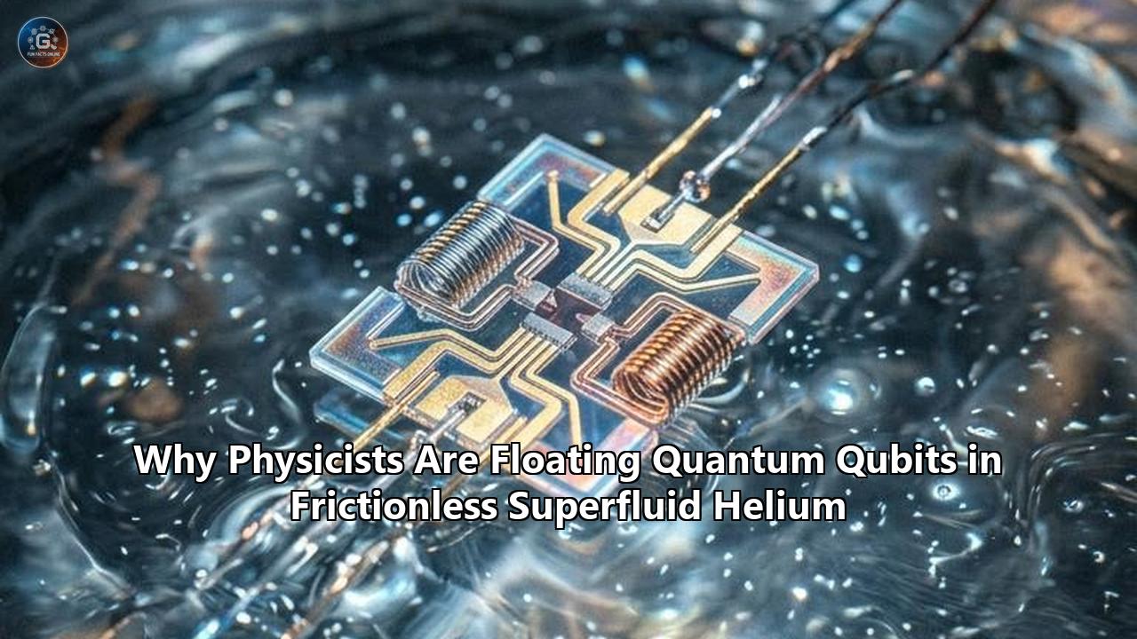
In physics laboratories in Chicago and East Lansing, single electrons are levitating ten nanometers above a pool of liquid helium chilled to within a fraction of a degree of absolute zero. Held in place by an electrostatic image charge and prevented from touching the liquid by a quantum barrier, these solitary particles represent an ambitious gambit in quantum hardware. The effort to build practical quantum processors has long been locked in a race dominated by superconducting circuits, trapped ions, and silicon quantum dots. Now, peer-reviewed validations from academic and industrial teams—spearheaded by researchers from Michigan State University, the University of Chicago, Stanford University, and the quantum startup EeroQ—have proved that individual electrons hovering over frictionless liquid helium can be manipulated, shuttled, and coupled to microwave photons using industry-standard silicon manufacturing.
The milestones arrived in quick succession. Experimental physics groups demonstrated the strong coupling of a single electron on helium to a superconducting microwave cavity, confirming that the motional state of an isolated electron on a liquid substrate can exchange energy quanta coherently with a photon. Concurrently, in Physical Review Applied, engineers reported the selective two-dimensional shuttling of electrons across a cryogenic chip fabricated on a commercial 130-nanometer complementary metal-oxide-semiconductor (CMOS) process line at SkyWater Technology. Over continuous automated testing, electron packets were transported across microchannel networks over aggregate distances exceeding tens of kilometers without the loss of a single charge. Backing these transport mechanics, experiments published in Physical Review X confirmed that single electrons can be trapped, sensed, and controlled on helium at 1.1 Kelvin—more than one hundred times higher than the ten-millikelvin operating thresholds demanded by standard superconducting transmons.
+-----------------------------------------------------------------------------------------+
|                                 PHYSICAL SYSTEM ANATOMY                                 |
|                                                                                         |
|       Vacuum (P < 10⁻¹⁰ Torr)                                                           |
|       ---------------------------------------------------------------------------       |
|                                                                                         |
|                           ( e⁻ )   <-- Single Electron Levitating                       |
|                             |          at z ≈ 7.6 nm - 10 nm                            |
|             Image Charge    |                                                           |
|             Attractive Force v                                                          |
|       ~~~~~~~~~~~~~~~~~~~~~~~~~~~~~~~~~~~~~~~~~~~~~~~~~~~~~~~~~~~~~~~~~~~~~~~~~~~       |
|       Superfluid ⁴He Film (~1 µm thick, T < 1.2 K)   [Zero Viscosity, Zero Spin]        |
|       ~~~~~~~~~~~~~~~~~~~~~~~~~~~~~~~~~~~~~~~~~~~~~~~~~~~~~~~~~~~~~~~~~~~~~~~~~~~       |
|                                                                                         |
|       [Dielectric / Microchannel Substrate: SiO₂ / Si]                                  |
|       [=================== DC Guard & Shuttling Gates ==========================]       |
|       [======= High-Impedance Resonator (TiN / Nb) / Readout Electrodes ========]       |
+-----------------------------------------------------------------------------------------+
These results have thrust an architecture originally theorized in the late 1990s into direct competition with the quantum industry's best-funded platforms. Building quantum qubits superfluid helium processors requires balancing radical isolation against practical accessibility. Proponents argue that using a liquid helium surface as an atomic-scale buffer solves the primary killer of quantum coherence in solid-state devices: material defects and charge noise. Critics and rival hardware developers contend that introducing a fluid interface creates hydrodynamic instabilities, limits gate speeds compared to pure transmons, and faces daunting packaging hurdles.
Understanding why elite laboratories are investing in floating electrons requires examining the physics of the helium-vacuum boundary and contrasting this emerging architecture against solid-state quantum circuits, trapped atomic ions, and solid noble-gas alternatives.
The Physics of the Floating Trap: Image Charges and Pauli Repulsion
The interface between vacuum and superfluid helium-4 creates a pristine trapping environment dictated by two competing physical forces. When an electron is introduced above the liquid surface, its presence polarizes the helium atoms beneath it. Liquid helium has an exceptionally low dielectric constant ($\epsilon \approx 1.0572$), slightly greater than the vacuum value of unity. Because $\epsilon > 1$, the electric displacement fields set up an attractive image-charge potential in the liquid. For an electron at a distance $z$ above the surface, this attractive potential mimics the classic one-dimensional Coulomb problem:
$$V_{\text{image}}(z) = -\frac{\Lambda e^2}{4\pi \epsilon_0 z}$$
where the effective charge scaling factor is governed by the dielectric mismatch:
$$\Lambda = \frac{\epsilon - 1}{4(\epsilon + 1)} \approx 0.00696$$
This weak electrostatic pull acts as an image force drawing the electron toward the liquid. If the substrate were water, silicon, or metal, the electron would crash into the surface, fall into a deep potential well, or bind chemically.
Helium-4 prevents this collapse through a fundamental quantum mechanical barrier. Helium is an inert noble gas with a closed $1s^2$ electronic shell. For an external electron to enter the liquid, it must occupy an empty quantum state within the helium atoms. By the Pauli exclusion principle, the incoming electron would have to occupy the orthogonal $2s$ conduction state, which requires overcoming an energy barrier of approximately 1.0 electron-volt ($V_0 \approx 1.0\text{ eV}$). Thermally, 1.0 eV corresponds to a temperature of more than 11,000 Kelvin—an insurmountable wall for an electron operating in a cryogenic apparatus below 2 Kelvin.
Energy Potential V(z)
     ^
1 eV |  [ HELIUM BULK (z < 0) ]    |   [ VACUUM (z > 0) ]
     |  Pauli Exclusion Barrier    |
     |  +-------------------------+ |
     |  |                         | |
     |  |                         | |
 0 eV+--+-------------------------+-+-----------------------------------> z (Distance)
     |                            |  \
     |                            |   \  Weak Image Potential:
     |                            |    \ V(z) = -Λe² / 4πε₀z
     |                            |     \
     |                            |      `-- (Ground State Level E₁ ≈ -7.6 K)
     |                            |          Hovering at z ≈ 7.6 nm
     v                            |
Trapped between an attractive image charge pulling it inward and an aggressive quantum exclusion barrier repelling it outward, the electron finds an equilibrium. It settles into quantized Rydberg-like energy states perpendicular to the liquid surface. In the perpendicular ($z$) coordinate, the bound states exhibit discrete energy levels:
$$E_n \approx -\frac{R_e}{n^2}, \quad n \in \{1, 2, 3, \dots\}$$
where the effective Rydberg constant for helium-4 is $R_e \approx 0.66\text{ meV}$, which translates to a transition frequency of approximately 130 to 150 gigahertz between the ground ($n=1$) and first excited ($n=2$) out-of-plane states. Crucially, the expectation value of the distance from the surface in the ground state is:
$$\langle z \rangle_1 \approx 7.6\text{ to }10\text{ nanometers}$$
The electron floats suspended in high vacuum, separated from any physical matter by a vacuum gap nearly twenty times wider than the helium interatomic spacing. In-plane lateral motion parallel to the surface ($x, y$) remains entirely unconstrained. The particle behaves as a genuine two-dimensional electron gas (2DEG) inhabiting a frictionless plane.
The Solid-State Bottleneck: Two-Level Systems and Dielectric Loss
To evaluate why researchers are willing to handle cryogenic liquid helium in microchannels, one must dissect the physical failure modes that plague established solid-state quantum computers.
Superconducting transmons—the foundation of hardware systems built by IBM, Google, and Rigetti—have carried quantum information processing from proof-of-principle devices to systems exceeding one thousand noisy physical qubits. Yet, transmons face fundamental materials science limits. A transmon is an LC circuit where the non-linear inductor is a Josephson junction consisting of two superconducting aluminum layers separated by an amorphous aluminum oxide ($\text{AlO}_x$) insulating barrier.
Amorphous dielectric materials are disordered. At millikelvin temperatures, atoms or small groups of atoms within the barrier, at metal-substrate interfaces, or on oxidized surfaces can tunnel between two nearly degenerate configuration states. These localized structural defects act as spurious quantum entities known as two-level systems (TLS). When the transition frequency of a TLS drifts into resonance with the qubit's operational frequency (typically 4 to 6 gigahertz), the TLS absorbs microwave energy from the qubit, precipitating energy relaxation characterized by the decay time $T_1$.
Furthermore, solid surfaces generate charge noise. Trapped charges in the underlying dielectric fluctuate randomly, generating fluctuating electric fields that shift the qubit's frequency and induce dephasing, characterized by the decoherence time $T_2^$. The quality factor $Q$ of superconducting microwave cavities and transmons is systematically capped by the dielectric loss tangent ($\tan\delta$) of the materials that construct them:
$$\frac{1}{Q_{\text{dielectric}}} = \sum_i p_i \tan \delta_i$$
where $p_i$ represents the electric field filling factor in the lossy dielectric region $i$. Even the most pristine silicon and sapphire wafers have native surface oxides and chemical residues that poison quantum states.
+---------------------------------------------------------------------------------------------------+
|                                  MATERIAL INTERFACE COMPARISON                                    |
+------------------------------------+--------------------------------------------------------------+
| SYSTEM                             | DOMINANT DECOHERENCE SOURCES                                 |
+------------------------------------+--------------------------------------------------------------+
| Superconducting Transmons          | * Amorphous AlOx junction defects (TLS)                      |
|                                    | * Surface oxides on sapphire/silicon (dielectric loss)       |
|                                    | * Non-equilibrium quasiparticle poisoning                   |
|                                    | * Macroscopic footprint sensitive to stray EM fields         |
+------------------------------------+--------------------------------------------------------------+
| Silicon Spin Qubits (Quantum Dots) | * Charge noise at Si/SiO₂ or Si/SiGe semiconductor interface|
|                                    | * Nuclear spin dephasing from ²⁹Si isotopes                  |
|                                    | * Valley-orbit splitting fluctuations                        |
|                                    | * Extreme sensitivity to nanometer gate lithography errors   |
+------------------------------------+--------------------------------------------------------------+
| Floating Electrons on Helium       | * Ripplons (capillary waves on the helium surface)           |
|                                    | * Thermal helium vapor atoms (negligible at T < 0.5 K)       |
|                                    | * Image-charge induced substrate dielectric noise (screened) |
|                                    | * ZERO substrate lattice defects; ZERO nuclear spin in ⁴He   |
+------------------------------------+--------------------------------------------------------------+
Silicon spin qubits, developed by researchers at Intel, QuTech, HRL Laboratories, and UNSW, compress the qubit footprint down to tens of nanometers by confining single electrons or holes inside electrostatic quantum dots defined within a silicon-silicon germanium ($\text{Si/SiGe}$) heterostructure or metal-oxide-semiconductor ($\text{Si-MOS}$) channel. While silicon spin qubits offer long spin coherence when isotopically purified to remove nuclear spin-bearing $^{29}\text{Si}$, they remain embedded inside a crystal lattice.
The moving electron interacts directly with the semiconductor interface. Fluctuating charge traps near the gate dielectric lead to charge noise, while strain and atomic-scale step edges perturb the semiconductor valley splitting. If the energy splitting between conduction band valleys is small or non-uniform across an array, qubit initialization fails and spin relaxation accelerates through spin-valley mixing.
Floating an electron on superfluid helium bypasses this condensed-matter environment entirely. Superfluid helium-4 at sub-kelvin temperatures is self-purifying; any chemical impurity—such as air, water, hydrogen, or nitrogen—freezes instantly and precipitates to the walls of the chamber. Helium-4 possesses an atomic nucleus with zero net nuclear spin ($I = 0$), eliminating the magnetic hyperfine dephasing that plagues group III-V semiconductors like gallium arsenide ($\text{GaAs}$). Because the electron levitates above the liquid in high vacuum, its wavefunction never intersects a disordered crystal lattice, an amorphous oxide, or a chemical contaminant. The dielectric loss tangent of liquid helium itself is vanishingly small ($\tan\delta < 10^{-10}$), providing a clean platform for harboring quantum qubits superfluid helium processors.
Liquid Helium vs. Solid Neon: The Battle Over Cryogenic Substrates
Within the noble-element quantum movement, an intense scientific debate has emerged regarding the physical state of the underlying substrate. Should the noble element remain a mobile, self-healing superfluid liquid, or should it be frozen into an immovable solid?
At the University of Notre Dame and Argonne National Laboratory, physicist Dafei Jin has pioneered the solid neon approach. Solid neon (eNe) qubits utilize single electrons trapped in vacuum above a frozen neon substrate. Neon condenses into a solid crystal at approximately 24.5 Kelvin under standard conditions and can be cooled to millikelvin temperatures inside a dilution refrigerator. Like helium, neon is an inert noble gas with a filled electronic shell, yielding a high vacuum barrier of roughly 0.67 eV that prevents electrons from penetrating the crystal.
+---------------------------------------------------------------------------------------------------+
|                        SUBSTRATE TRADEOFF MATRIX: SOLID NEON VS. SUPERFLUID HELIUM               |
+-----------------------------------+-------------------------------+-------------------------------+
| METRIC / PROPERTY                 | SOLID NEON (eNe)              | SUPERFLUID HELIUM (eHe)       |
+-----------------------------------+-------------------------------+-------------------------------+
| Physical Phase                    | Frozen Solid Polycrystal      | Quantum Superfluid Liquid     |
+-----------------------------------+-------------------------------+-------------------------------+
| Substrate Coherence Limits        | Mechanical rigidity suppresses| Ripplons (quantized capillary |
|                                   | surface waves (no ripplons)   | waves) cause phase jitter     |
+-----------------------------------+-------------------------------+-------------------------------+
| Surface Morphology                | Rough; contains bumps, grain  | Atomically smooth meniscus;   |
|                                   | boundaries, and nanovoids     | self-healing liquid surface   |
+-----------------------------------+-------------------------------+-------------------------------+
| Qubit Mobility & Transport        | Immobile; pinned by local     | Fully mobile; scalable        |
|                                   | surface potential variations  | CCD-style 2D shuttling        |
+-----------------------------------+-------------------------------+-------------------------------+
| Demonstrated Coherence (Charge)   | T₁ ≈ 100 µs, T₂ ≈ 100 µs      | T₁ ≈ 10–100 µs (orbital)      |
+-----------------------------------+-------------------------------+-------------------------------+
| Predicted Coherence (Spin)        | > 1–10 seconds                | > 10–100 seconds              |
+-----------------------------------+-------------------------------+-------------------------------+
| Manufacturing Tolerances          | Deposition requires precise   | Capillary filling in standard |
|                                   | in-situ cryogenic annealing   | foundry-fabricated microfluidics|
+-----------------------------------+-------------------------------+-------------------------------+
The fundamental thesis for choosing solid neon over liquid helium centers on surface vibrations. A liquid surface, even when superfluid, supports capillary waves and surface gravity modes. In the quantum regime, quantized capillary waves are called ripplons. Ripplons act as two-dimensional surface phonons that propagate across the helium layer. When an electron floats above liquid helium, its vertical distance to the surface fluctuates due to the zero-point and thermal motion of these ripplons. Because the image potential depends inversely on distance ($1/z$), these surface ripples modulate the binding energy of the electron, inducing orbital dephasing and mechanical jitter.
Solid neon eliminates ripplons. Because it is a rigid solid, there are no capillary waves. In 2022 and 2024, Jin’s team published findings demonstrating that an electron charge qubit on solid neon could achieve energy relaxation times $T_1$ and dephasing times $T_2$ exceeding 100 microseconds—several orders of magnitude longer than conventional semiconductor charge qubits, which typically decohere in nanoseconds due to material charge noise.
However, solid neon introduces its own structural liabilities. Freezing a noble gas inside a cryogenic chamber onto a microchip does not yield an ideal single crystal; instead, it forms an imperfect, polycrystalline film laced with surface roughness, grain boundaries, and nanoscale steps. Recent theoretical and experimental analyses confirm that local bumps and depressions in the solid neon film perturb the electrostatic potential. Electrons become pinned in topographical local minima.
This pinning destroys one of the most powerful capabilities of floating electrons: long-distance mobility. In solid neon, moving an electron requires forcing it across physical surface ridges, which scrambles its quantum state or demands prohibitive gate voltages. Furthermore, growing an atomically flat solid neon layer uniformly across an entire multi-qubit chip inside a cryostat has proved notoriously difficult to replicate consistently.
Superfluid helium solves the topography problem through fluid dynamics and surface tension. Superfluid helium-4 possesses zero viscosity, allowing it to coat microfabricated chips via capillary action. Surface tension pulls the liquid into an atomically smooth meniscus. If a disturbance or localized cosmic ray impacts the liquid, the superfluid redistributes instantly to reform a pristine, self-healing interface.
Engineers at Michigan State University, Stanford, and EeroQ mitigate the ripplon problem by confining the helium inside narrow, microfabricated channels. When liquid helium is confined within microchannels roughly one to two micrometers wide and a few hundred nanometers deep, long-wavelength ripplons are geometrically suppressed. The capillary dispersion relation shifts the fundamental vibration modes to much higher frequencies, freezing them out at operating temperatures and leaving behind a quiescent, ultra-smooth liquid foundation.
The Four-Way Hardware Divergence: Electrons on Helium vs. Dominant Architectures
To assess the practical value of levitating quantum qubits superfluid helium devices, the platform must be benchmarked across key performance vectors against superconducting circuits, semiconductor spin dots, and trapped-ion systems.
+-------------------------------------------------------------------------------------------------------------------------------+
|                                      COMPREHENSIVE HARDWARE ARCHITECTURE COMPARISON                                           |
+------------------------+-----------------------+-----------------------+-----------------------+------------------------------+
| ATTRIBUTE              | SUPERCONDUCTING       | SEMICONDUCTOR         | TRAPPED IONS          | ELECTRONS ON SUPERFLUID      |
|                        | TRANSMONS             | SPIN QUBITS           | (e.g., Ba⁺, Yb⁺)      | HELIUM                       |
+------------------------+-----------------------+-----------------------+-----------------------+------------------------------+
| Qubit Dimension        | Macroscopic:          | Nanoscopic:           | Atomic:               | Intermediate:                |
|                        | ~100 µm – 1 mm        | ~50 – 100 nm          | Zero-dimension point  | ~0.5 – 2 µm                  |
+------------------------+-----------------------+-----------------------+-----------------------+------------------------------+
| Coherence Time         | T₁ ≈ 50 – 400 µs      | T₂* ≈ 10 – 100 µs     | T₂ > 1 – 60 seconds   | T₂ > 10 – 100 seconds        |
|                        | T₂ ≈ 50 – 300 µs      | T₂ (echo) ≈ 1 – 20 ms |                       | (spin state, predicted)      |
+------------------------+-----------------------+-----------------------+-----------------------+------------------------------+
| Single-Qubit Gate Time | Ultra-fast:           | Fast:                 | Slow:                 | Ultra-fast:                  |
|                        | ~10 – 30 ns           | ~20 – 100 ns          | ~1 – 50 µs            | ~10 – 50 ns (microwave-driven)|
+------------------------+-----------------------+-----------------------+-----------------------+------------------------------+
| Two-Qubit Gate Time   | ~30 – 100 ns          | ~50 – 200 ns          | ~50 – 500 µs          | ~20 – 100 ns                 |
|                        | (cross-resonance)     | (exchange interaction)| (Mølmer-Sørensen)     | (Coulomb / Exchange)         |
+------------------------+-----------------------+-----------------------+-----------------------+------------------------------+
| Connectivity Scheme    | Fixed nearest-neighbor| Short-range arrays;   | Dynamic shuttling /   | Dynamic 2D CCD shuttling;    |
|                        | planar mesh (heavy SWAP) dense gate wiring    | all-to-all connectivity| all-to-all chip connectivity |
+------------------------+-----------------------+-----------------------+-----------------------+------------------------------+
| Operating Temperature  | 10 – 20 mK            | 50 – 1000 mK          | Room Temp / 4 K       | 10 mK – 1.1 K                |
|                        | (Dilution fridge)     | (Dilution fridge)     | (Laser / RF trap)     | (Standard ⁴He cryostat)      |
+------------------------+-----------------------+-----------------------+-----------------------+------------------------------+
| Manufacturing Source   | Specialized cleanroom | Semiconductor CMOS    | Micro-machined traps  | Standard Commercial CMOS     |
|                        | lithography (Al/Nb)   | foundry (Si/Ge)       | + Bulk optical lasers | Foundries (130 nm node)      |
+------------------------+-----------------------+-----------------------+-----------------------+------------------------------+
1. Physical Footprint and Scaling Geometry
Superconducting transmons suffer from physical scale. A transmon is macroscopic, requiring large interdigitated capacitor pads to generate enough capacitance ($C_s \approx 60\text{ to }100\text{ fF}$) to suppress charge noise, giving it a footprint spanning hundreds of micrometers. Fitting one million transmons onto a single silicon chip would require a processor larger than a dining room table, making cryostat integration impossible without optical or microwave interconnects between modular dilution refrigerators.
Silicon spin qubits occupy the opposite extreme: their quantum dots are spaced less than 100 nanometers apart. While this allows extreme density, it introduces a severe routing crisis. Thousands of high-frequency control lines must terminate in a footprint the size of a red blood cell, producing parasitic cross-talk and thermal dissipation that overwhelms the cooling budget of standard dilution refrigerators.
Electrons on helium occupy an engineering sweet spot. The lateral spatial extent of a single electron's wavefunction in a microchannel trap is approximately 50 to 100 nanometers, but the lithographic trap pitch is typically between 0.5 and 2 micrometers. This spacing provides enough room to route standard CMOS metal interconnects without cross-talk, while maintaining a density thousands of times higher than superconducting transmons.
2. Connectivity: Fixed Planar Grids vs. All-to-All Shuttling
In a superconducting quantum processor, qubits are permanently anchored to fixed physical locations on a 2D surface (such as the heavy-hex lattice of IBM's Quantum Heron chips). Qubit A can only interact directly with Qubit B if they share a physical coupling element. To run an algorithm where non-adjacent qubits must become entangled, the quantum compiler must execute long chains of SWAP gates. Each SWAP gate consumes coherence budget and compounds error rates.
Trapped-ion processors (developed by Quantinuum and IonQ) avoid this by mechanically moving their qubits. In a quantum charge-coupled device (QCCD) architecture, atomic ions (such as ytterbium or barium) are physically shuttled through radio-frequency potential channels using time-varying voltages. This allows arbitrary all-to-all connectivity: any ion can be transported into an interaction zone to undergo a gate operation with any other ion. However, ions are heavy particles (hundreds of thousands of times more massive than an electron). Accelerating an ion too quickly heats its secular motion, requiring complex laser sideband cooling and capping gate speeds in the microsecond-to-millisecond range.
Electrons on superfluid helium combine the mechanical transportability of trapped ions with the speed of solid-state circuits. Because the electron is an elementary particle with minimal mass, it can be shuttled at velocities exceeding tens of thousands of meters per second with negligible motional heating. This eliminates the need for laser recooling.
The recent demonstration of parallel, selective 2D shuttling across 128 microchannels in a CMOS device proves that electrons can be continuously moved between memory zones, gate zones, and readout resonators. This grants the platform all-to-all connectivity while executing gate operations at gigahertz microwave clock rates.
Dual Encoding: Orbital States vs. Pure Spin
A pivotal question facing researchers working with floating electrons is which physical degree of freedom to use as the computational basis. The system offers two choices: the orbital (motional) state or the intrinsic electron spin state.
                +-----------------------------------------------------------+
                |             THE DUAL-ENCODING DESIGN LANDSCAPE            |
                +-----------------------------------------------------------+
                                             |
             +-------------------------------+-------------------------------+
             |                                                               |
             v                                                               v
   [ MOTIONAL / ORBITAL QUBIT ]                                    [ INTRINSIC SPIN QUBIT ]
   Basis: Lateral Harmonic States                                 Basis: Magnetic Zeeman States
   |0⟩ = Ground Motional State |ψ₀⟩                               |0⟩ = Spin-Up |↑⟩
   |1⟩ = First Excited State   |ψ₁⟩                               |1⟩ = Spin-Down |↓⟩
   ---------------------------------                              ---------------------------------
   • Direct dipole coupling to RF                                 • Zero electric dipole moment
   • Ultrafast gates: ~1 - 5 ns                                   • Extreme coherence: T₂ > 10 - 100 s
   • Direct cQED cavity readout                                   • Immunity to electric charge noise
   • Vulnerable to ripplon jitter                                 • Requires synthetic spin-orbit coupling
   • Primary use: Readout & bus                                   • Primary use: Robust quantum memory
1. The Motional / Orbital Qubit
When a single electron is laterally confined within a microchannel by electrostatic guard electrodes and a pair of underlying barrier gates, it sits in a lateral potential well. To first approximation, this well is a harmonic oscillator:
$$V(x, y) = \frac{1}{2} m_e \omega_x^2 x^2 + \frac{1}{2} m_e \omega_y^2 y^2$$
By adjusting the shaping electrodes, engineers introduce intentional geometric anharmonicity, creating non-equidistant energy spacings. The ground state $|0\rangle$ and first excited motional state $|1\rangle$ serve as the qubit basis.
The motional state possesses a massive electric dipole moment ($d = e \langle 0 | x | 1 \rangle$). As a result, the orbital state couples directly to the transverse electric fields of an on-chip superconducting microwave resonator. The interaction is described by the canonical Jaynes-Cummings Hamiltonian:
$$\hat{H} = \hbar \omega_r \left( \hat{a}^\dagger \hat{a} + \frac{1}{2} \right) + \frac{1}{2} \hbar \omega_q \hat{\sigma}_z + \hbar g \left( \hat{a}^\dagger \hat{\sigma}_- + \hat{a} \hat{\sigma}_+ \right)$$
where $\omega_r$ is the resonator frequency, $\omega_q$ is the electron orbital transition frequency, and $g$ is the electron-photon coupling strength.
In the milestone experiment reported by EeroQ, Schuster, and collaborators, researchers reached the strong-coupling regime where the coupling rate $g/2\pi$ (several megahertz) significantly outpaces both the resonator photon decay rate $\kappa/2\pi$ and the electron dephasing rate $\gamma/2\pi$:
$$g \gg (\kappa, \gamma)$$
Reaching strong coupling enables dispersive quantum non-demolition (QND) readout: shifting the electron's quantum state shifts the natural resonance frequency of the microwave cavity, allowing state detection in a few hundred nanoseconds using standard homodyne microwave electronics. However, because the orbital state interacts strongly via electric fields, it remains susceptible to electrostatic fluctuations and ripplons, limiting its pure coherence time to between tens of microseconds and a few milliseconds.
2. The Intrinsic Spin Qubit
To achieve coherence times capable of supporting fault-tolerant quantum error correction without continuous hardware intervention, physicists map quantum information to the electron's fundamental spin:
$$|0\rangle \equiv |\!\uparrow\rangle, \quad |1\rangle \equiv |\!\downarrow\rangle$$
The electron spin is isolated from its environment. The electron has no internal charge distribution that can couple to electric fields; it interacts with the universe almost exclusively through its magnetic dipole moment:
$$\vec{\mu}_s = -g_e \mu_B \vec{S}$$
Because the underlying helium-4 atoms have zero nuclear magnetic moments and the electron is floating in vacuum, there are no nuclear spins to induce Overhauser field fluctuations. Theoretical models indicate that the spin relaxation time $T_1$ for an electron on liquid helium exceeds hours, while the spin coherence time $T_2$ is projected to surpass 10 to 100 seconds.
3. The Synthetic Spin-Orbit Bridge
The challenge with spin qubits is the inverse of their virtue: because the electron spin does not couple to electric fields, it cannot couple directly to the electric fields of a microwave cavity for fast readout or two-qubit operations. Relying strictly on magnetic dipole interactions for control would limit gate speeds to the megahertz range, which is far too slow to capitalize on the system's inherent advantages.
                           SYNTHETIC SPIN-ORBIT COUPLING

      B₀ (Static DC Field)                 Microwave Electric Field E_rf(t)
             |                                          |
             v                                          v
      +--------------+    Slanting Gradient B_grad(x)  +------------------+
      | Electron     |  <============================> | Lateral Motion   |
      | Spin State   |       Micro-Ferromagnet         | In Harmonic Well |
      | |↑⟩  vs  |↓⟩ |                                 | |ψ₀⟩  vs  |ψ₁⟩   |
      +--------------+                                 +------------------+
             ^                                                  ^
             |                                                  |
             +============= Hybridized Spin-Charge State =======+
                                       |
                                       v
               Fast Microwave Control & Cavity Readout via Motional Dipole!
To resolve this trade-off, experimental designs introduce synthetic spin-orbit coupling via on-chip micromagnet arrays. Engineers lithographically pattern cobalt, nickel, or permalloy ferromagnetic micropillars adjacent to the microchannel traps. When magnetized by an external magnetic field $B_0$, these structures create a steep magnetic field gradient:
$$b_x = \frac{\partial B_z}{\partial x}$$
As the electron oscillates in its lateral electrostatic trap along the $x$-direction with velocity $\vec{v}$, it experiences an effective time-dependent magnetic field in its rest frame:
$$\vec{B}_{\text{eff}}(t) = b_x \, x(t) \, \hat{z}$$
This local gradient couples the electron's spatial position $x$ directly to its Pauli spin matrix $\hat{\sigma}_z$. This interaction hybridizes the spin state with the motional orbital state:
$$\hat{H}_{\text{SOC}} = g_{\text{so}} \left( \hat{a} + \hat{a}^\dagger \right) \left( \hat{\sigma}_+ + \hat{\sigma}_- \right)$$
Through this engineered hybridization, the quantum information rests in the spin state (shielded from decoherence), but can be manipulated and read out through the orbital dipole moment using gigahertz microwave pulses applied to the cavity. By selectively tuning the electron in and out of resonance with the field gradient using gate voltages, researchers can turn the interaction on for nanosecond gate operations and turn it off during idling, safeguarding the long spin coherence time.
Thermal Economics: Smashing the Millikelvin Barrier
One of the most consequential findings to emerge from recent floating-electron experiments is operational viability above 1 Kelvin.
Dilution refrigerators—the massive, gold-plated cryostats that encase superconducting and silicon quantum processors—rely on mixing two isotopes of helium ($^3\text{He}$ and $^4\text{He}$) to cool their mixing chambers down to 10 to 20 millikelvin. At these temperatures, cooling power is scarce. A high-end commercial dilution refrigerator provides roughly 10 to 25 microwatts of cooling capacity at 20 millikelvin, and scarcely 500 microwatts at 100 millikelvin.
Every coaxial line running from room-temperature control racks down into the cryostat introduces heat through thermal conduction and radio-frequency attenuation. As processor counts grow from dozens of qubits to tens of thousands, the thermal budget becomes a hard physical ceiling. Transmon qubits must be maintained below 20 millikelvin because their energy transitions correspond to frequencies around 5 gigahertz ($\sim 240\text{ mK}$). If the environmental temperature rises toward 100 millikelvin, thermal photons populate the microwave cavities:
$$n_{\text{th}} = \frac{1}{\exp\left(\frac{h\nu}{k_B T}\right) - 1}$$
These thermal photons destroy qubit states, inducing spontaneous excitation and dephasing.
Cryostat Temperature vs. Available Cooling Power
Cooling Power
     ^
10 W |                                                [ 1 K - 4.2 K Operations ]
     |                                                * ⁴He Evaporative Cryocoolers
 1 W |                                                * Multi-Watt Cooling Budget
     |                                                * Co-packaged Cryo-CMOS Drivers
     |                                                * Thousands of RF Lines Tolerated
10 mW+------------------------------------------------+
     |
 1 mW|                        [ 100 mK Regime ]
     |                        * Limited Dissipation
10 µW|   [ 10 - 20 mK Regime ]
     |   * Superconducting Transmons & Si Spin Qubits
 1 µW|   * Max ~20 µW Cooling Budget
     |   * Extreme Wiring & Thermal Bottleneck
     +---+--------------------+-----------------------+--------------> Temperature
        10 mK                100 mK                   1 K
In the Physical Review X experiment, researchers trapped, controlled, and read out individual electrons on superfluid helium at 1.1 Kelvin. This represents a temperature more than one hundred times warmer than typical superconducting qubit operating levels.
The physics permitting this thermal elevation stems from two factors:
- Trap Depth and Rydberg Transitions: The out-of-plane binding energy of the electron to the helium surface is roughly 7.6 Kelvin in temperature units. The barrier against penetrating into the liquid is 1.0 eV ($\sim 11,600\text{ K}$). Consequently, raising the bath temperature from 10 millikelvin to 1.1 Kelvin does not cause the electron to desorb or plunge into the fluid. It remains trapped in its out-of-plane ground state.
- Coupling Dynamics in High-Impedance Resonators: By fabricating microwave resonators from thin-film superconductors with high kinetic inductance—such as titanium nitride (TiN) or granular aluminum—the characteristic impedance $Z_0$ of the circuit can be pushed above 1,000 ohms, far higher than the standard 50-ohm transmission line. The vacuum electric field fluctuation scales as:
$$E_{\text{rms}} \propto \omega_r \sqrt{\frac{\hbar Z_0}{2}}$$
This large impedance boosts the single-electron-photon coupling rate $g$, allowing coherent interaction signals to stand out clearly against elevated thermal noise floors.
Operating at 1.1 Kelvin transforms the cryogenic economics of quantum computing. At 1 Kelvin, cooling is achieved using closed-cycle, pulse-tube pumped $^4\text{He}$ cryostats, which completely eliminate the need for rare, expensive helium-3 mixtures. More importantly, available cooling power at 1.1 Kelvin scales to hundreds of milliwatts or even full watts—more than four orders of magnitude higher than a dilution refrigerator's mixing chamber.
This generous cooling capacity allows classical CMOS digital control logic, analog-to-digital converters, and microwave multiplexers to be mounted directly alongside the quantum chip on the 1-Kelvin cold plate, breaking the cryogenic wiring bottleneck that limits other solid-state platforms.
Shuttling Dynamics: CCD Architectures for Quantum Processors
The primary practical impediment to scaling quantum chips is routing: connecting arbitrary pairs of qubits across a large 2D surface to execute entangling two-qubit gates without running millions of physical coaxial cables into the refrigerator.
The floating-electron architecture addresses this via electrostatic shuttling across microchannel capillary networks.
+---------------------------------------------------------------------------------------------------+
|                           2D CCD-STYLE QUANTUM SHUTTLING ARCHITECTURE                             |
+---------------------------------------------------------------------------------------------------+
|                                                                                                   |
|    Microchannel filled with superfluid ⁴He (~1.5 µm wide)                                         |
|    ===========================================================================================    |
|    [Gate V₁]       [Gate V₂]       [Gate V₃]       [Gate V₁]       [Gate V₂]       [Gate V₃]      |
|    -------------------------------------------------------------------------------------------    |
|        \               /               |               |               |               |          |
|         \  e⁻ Packet  /                |               |               |               |          |
|          \___________/                 |               |               |               |          |
|                                                                                                   |
|    Step 1: Electron localized above Gate V₂ (Potential Well)                                      |
|    -------------------------------------------------------------------------------------------    |
|                                        |                                                          |
|    Step 2: Voltage on V₃ lowered; V₂ raised:                                                      |
|                                        |                                                          |
|    -------------------------------------------------------------------------------------------    |
|    [Gate V₁]       [Gate V₂]       [Gate V₃]       [Gate V₁]       [Gate V₂]       [Gate V₃]      |
|    -------------------------------------------------------------------------------------------    |
|                        \               /                                                          |
|                         \  e⁻ Shuttled/                                                           |
|                          \___________/                                                            |
|                                                                                                   |
|    Continuous 3-phase clocking moves electrons smoothly along channels at > 10,000 m/s             |
+---------------------------------------------------------------------------------------------------+
Using standard foundry manufacturing at SkyWater Technology, engineers developed chips featuring networks of microchannels interconnected by arrays of sub-surface titanium nitride and aluminum gate electrodes. Liquid helium fills these channels automatically through capillary draw. A low-temperature electron source (such as a tungsten filament or field-emission tip) pulses electrons into the reservoir zones.
Once trapped on the liquid surface, electrons are transported using multi-phase clocking voltages applied to the underlying gates, identically to how charge packets are clocked across pixels in a classic Charge-Coupled Device (CCD) image sensor:
- Three-Phase Clocking Potentials: By cycling gate voltages $(V_1, V_2, V_3)$ in overlapping sinusoidal or trapezoidal patterns, an electrostatic potential well translates smoothly down the length of the microchannel. The floating electron slides across the frictionless superfluid helium surface, locked in the moving potential trough.
- Lossless, Long-Distance Transfer: In the Physical Review Applied study, electrons were transferred billions of consecutive times across 128 microchannels, racking up tens of kilometers of total distance without detectable electron loss or spontaneous ejection from the trap. Because superfluid helium has zero viscosity, hydrodynamic friction is absent. The only theoretical velocity ceiling is the Landau critical velocity of superfluid $^4\text{He}$ ($v_c \approx 50\text{ m/s}$), above which the moving electron can dissipate energy by creating quantized vortex rings or roton excitations.
- Decoupled Functionality Zones: Shuttling allows processor architectures to decouple memory, processing, and readout into physically dedicated chip zones:
Storage Registers: Dense, quiet arrays where electron spins idle in magnetic shielding away from noisy control lines.
Interaction Zones: Localized regions equipped with ferromagnetic micropillars where electrons are brought together to undergo two-qubit exchange gates or magnetic gradient operations.
Readout Ports: Resonant cavity ports where single electrons are shuttled to undergo dispersive state measurement, then returned to the processing queue.
This architectural modularity reduces wire counts. Instead of provisioning dedicated microwave drive and readout lines for every physical qubit, a modest set of shared control buses can manipulate and read millions of electrons dynamically shuttled across the processor.
Two-Qubit Interactions: Coulomb Exchange in Microfluidic Geometries
While single-qubit rotations and long-range transport have been experimentally validated, a viable quantum platform requires high-fidelity two-qubit entangling gates.
Floating electrons on helium provide two distinct mechanisms for engineering two-qubit gates: direct Coulomb interactions and coherent photon-mediated cavity exchange.
+---------------------------------------------------------------------------------------------------+
|                               TWO-QUBIT GATE IMPLEMENTATION MODES                                 |
+---------------------------------------------------------------------------------------------------+
| MODE A: DIRECT COULOMB EXCHANGE (Local, Fast)                                                     |
|                                                                                                   |
|           [Electron 1] <======== Coulomb Repulsion ========> [Electron 2]                         |
|             ( e₁⁻ )             F = e² / 4πε₀r²               ( e₂⁻ )                             |
|          ~~~~~~~~~~~~~                                     ~~~~~~~~~~~~~                          |
|         ~~~~~~~~~~~~~~~~~~~~ Superfluid ⁴He Film ~~~~~~~~~~~~~~~~~~~~~~~~                         |
|                                                                                                   |
|    * Unscreened Coulomb force couples motional wavefunctions directly.                            |
|    * Tuning central gate V_barrier controls wavefunction overlap & exchange splitting J.           |
|    * Two-qubit √SWAP or CPHASE executed in ~10 - 50 ns.                                           |
+---------------------------------------------------------------------------------------------------+
| MODE B: CAVITY-MEDIATED EXCHANGE (Long-Range, Distributed)                                        |
|                                                                                                   |
|         [ e₁⁻ ] <--- g ---> [ Superconducting Resonator ] <--- g ---> [ e₂⁻ ]                     |
|                                                                                                   |
|    * Virtual microwave photons in a shared coplanar waveguide act as the interaction bus.         |
|    * Enables arbitrary coupling between qubits separated by millimeters across the chip.          |
|    * Virtual exchange Hamiltonian: H_eff = (ħg² / Δ) (σ₁⁺ σ₂⁻ + σ₁⁻ σ₂⁺).                         |
+---------------------------------------------------------------------------------------------------+
1. Direct Coulomb / Exchange Interactions
Unlike electrons in semiconductor quantum dots, where the high dielectric constant of the material (e.g., $\epsilon \approx 11.7$ for silicon, $\epsilon \approx 13.1$ for gallium arsenide) heavily screens electric fields, electrons hovering over liquid helium experience minimal screening ($\epsilon \approx 1.057$). The Coulomb repulsion between two trapped electrons is raw and long-ranged:
$$U_C(r) = \frac{e^2}{4\pi \epsilon_{\text{eff}} r}$$
When two single electrons are brought into adjacent potential wells separated by a sub-micron barrier electrode, their motional states become coupled by Coulomb force. If the barrier potential between the wells is lowered via gate voltage, the spatial wavefunctions of the two electrons overlap, turning on the quantum mechanical exchange interaction:
$$\hat{H}_{\text{exchange}} = J(t) \, \vec{S}_1 \cdot \vec{S}_2$$
The exchange energy $J(t)$ scales exponentially with the barrier height and inter-qubit separation. Modulating $J(t)$ via gate pulses enables fundamental two-qubit entangling operations—such as $\sqrt{\text{SWAP}}$ or Controlled-PHASE ($\text{CZ}$) gates—in 10 to 50 nanoseconds.
2. Cavity-Mediated Photon Exchange
For electrons separated by large physical distances, two-qubit entanglement can be mediated by a shared superconducting coplanar waveguide resonator.
When two electrons are coupled to the same microwave cavity mode with coupling strengths $g_1$ and $g_2$, but both are detuned from the cavity frequency by $\Delta = \omega_q - \omega_r$ such that $|\Delta| \gg g$, direct photon absorption is suppressed. Instead, the electrons exchange virtual photons through the vacuum field of the resonator. This generates an effective long-range flip-flop interaction:
$$\hat{H}_{\text{eff}} = \frac{\hbar g_1 g_2}{\Delta} \left( \hat{\sigma}_1^+ \hat{\sigma}_2^- + \hat{\sigma}_1^- \hat{\sigma}_2^+ \right)$$
This cavity-bus architecture allows two electrons positioned at opposite ends of a microfluidic channel to entangle without physically moving them together, mirroring the long-distance entanglement techniques perfected in superconducting circuit architectures.
Engineering Hurdles and Remaining Questions
Despite these experimental milestones, the road toward a commercially viable quantum qubits superfluid helium computing platform remains crowded with formidable physics and materials challenges.
+---------------------------------------------------------------------------------------------------+
|                                 UNRESOLVED ENGINEERING HURDLES                                    |
+------------------------------------+--------------------------------------------------------------+
| CHALLENGE                          | PHYSICAL MECHANISM & IMPACT                                  |
+------------------------------------+--------------------------------------------------------------+
| Cryogenic Mechanical Microphonics  | Pulse-tube cryocooler vibrations generate micro-ripplons on  |
|                                    | the helium film, causing phase noise in motional states.     |
+------------------------------------+--------------------------------------------------------------+
| Microfluidic Film Uniformity       | Maintaining stable nanometer-scale liquid film thickness      |
|                                    | across centimeters of chip space requires hermetic sealing   |
|                                    | and active superfluid capillary volume management.           |
+------------------------------------+--------------------------------------------------------------+
| High-Fidelity Entangling Gates     | While single-electron trapping, shuttling, and cavity        |
|                                    | readout are proven, two-qubit gate fidelities (>99.5%)       |
|                                    | have yet to be benchmarked experimentally in the laboratory. |
+------------------------------------+--------------------------------------------------------------+
| Thermomechanical Packaging         | Integrating microwave feedlines, DC CMOS clocking, and       |
|                                    | liquid helium fill-capillaries within a vacuum-tight,        |
|                                    | magnetically shielded enclosure without introducing heat.   |
+------------------------------------+--------------------------------------------------------------+
1. Mechanical Microphonics and Surface Dynamics
The primary operational concern remains cryogenic vibration. Modern dry cryostats use mechanical pulse tubes to achieve sub-Kelvin temperatures. The cyclic compression and expansion of helium gas in these coolers produces mechanical vibrations at frequencies ranging from 1 to 50 hertz.
On a liquid substrate, these mechanical shocks propagate into the microchannels, exciting low-frequency surface sloshing and capillary oscillations. While capillary geometry suppresses long-wavelength modes, sub-hertz and low-kilohertz ripplons can alter the instantaneous distance between the electron and the underlying gates, introducing phase jitter into gate operations. Solving this requires advanced passive and active vibration-isolation systems and microchannel architectures engineered to damp surface oscillations hydrodynamically.
2. Film Level Control and Hermetic Sealing
Superfluid helium exhibits the Rollin film effect: it creeps up the walls of any container that houses it, forming a microscopic film approximately 30 nanometers thick that migrates toward warmer regions.
Maintaining a constant, uniform liquid film thickness across a complex CMOS chip containing thousands of microchannels requires precise fluidic engineering. If the helium level drops too low, the electron's distance to the chip surface shrinks, exposing it to dielectric surface noise. If the liquid overflows the microchannels, lateral electrostatic confinement fails. Teams must package their chips inside hermetically sealed silicon micro-cavities where helium fill levels are controlled by on-chip capillary reservoirs and capacitive liquid-level sensors.
3. Demonstrating Fault-Tolerant Gate Fidelities
The most critical upcoming scientific milestone is not shuttling or trapping, but the experimental measurement of two-qubit gate fidelity via randomized benchmarking. Superconducting qubits have demonstrated two-qubit gate fidelities exceeding 99.8%, while trapped-ion systems routinely cross 99.9%.
For electrons on helium, theoretical blueprints predict gate fidelities well above the 99% fault-tolerance threshold due to the absence of TLS defects. However, this must be proven experimentally under actual laboratory noise conditions. Until an experimental group executes a verified two-qubit entangling gate between two individual electrons on helium, the platform remains an emerging contender rather than a confirmed commercial rival.
What to Watch Next: The Trajectory of Floating Qubits
The timeline for floating-electron quantum computing is accelerating rapidly as theoretical concepts yield to empirical devices. With strong microwave coupling and scalable CMOS shuttling validated by peer-reviewed research, several upcoming milestones will determine whether the platform can break into quantum computing's top tier:
- Demonstration of Coherent Spin Control via Synthetic Spin-Orbit Coupling: Experimental realization of single-qubit spin rotations driven by ferromagnetic field gradients, confirming whether predicted spin coherence times ($T_2 > 10\text{ seconds}$) hold in functional silicon devices.
- Execution of the First Coherent Two-Qubit Gate: Demonstration of exchange-based or cavity-mediated entanglement between two floating electrons on helium, with fidelity benchmarking via quantum state tomography.
- Integration of On-Chip Cryo-CMOS Clock Generation: Exploiting operation at 1.1 Kelvin by fabricating 3-phase CCD shuttling clock generators directly onto the qubit die, shrinking control hardware to a handful of digital input pins.
- Consolidation or Coexistence with the Solid Neon Camp: Tracking whether solid-substrate approaches (eNe) resolve their polycrystalline surface defect issues, or if the self-healing, mobile nature of superfluid helium establishes itself as the winning noble-element substrate.
Floating electrons over frictionless superfluid helium challenge the conventional wisdom that quantum processors must rely either on fixed, defect-prone solid-state junctions or complex, laser-trapped atomic clouds. By capturing the atomic-scale simplicity and pristine coherence of free electrons while directing them across silicon circuits using standard microfluidic channels, researchers have established a unique third pathway. The physics indicates that when you decouple a quantum qubit from the imperfections of solid matter, the path toward a scalable quantum computer becomes significantly smoother.
Reference:
- https://postquantum.com/quantum-research/above-1-k-qubits/
- https://schusterlab.stanford.edu/static/pdfs/Koolstra2019.pdf
- https://arxiv.org/html/2509.14506v1
- https://www.techexplorist.com/quantum-computing-breakthrough-electrons-helium/103301/
- https://www.eeroq.com/eeroq-develops-new-microwave-resonators-for-our-future-quantum-processors/
- https://quantumcomputingreport.com/eeroq-advances-its-electron-on-helium-ehe-qubit-technology/
- https://www.eeroq.com/eeroq-electron-shuttling-achievements-published-in-physical-review-applied/
- https://www.eeroq.com/publications/
- https://pubmed.ncbi.nlm.nih.gov/10373109/
- https://arxiv.org/pdf/2311.02501
- https://www.researchgate.net/publication/385746919_Superfluid_Helium_for_Advanced_Quantum_Computing_Architectures
- https://en.wikipedia.org/wiki/Electron-on-helium_qubit