The global search for a material that can transmit electricity with absolutely zero energy loss has taken a decisive, prize-winning turn. On June 10, 2026, the Norwegian Academy of Science and Letters announced that the prestigious Kavli Prize in Nanoscience was awarded to Eva Andrei of Rutgers University, Pablo Jarillo-Herrero of the Massachusetts Institute of Technology (MIT), and Allan MacDonald of the University of Texas at Austin. The trio was honored for their pioneering development of "twistronics"—the practice of stacking and rotating atomically thin layers of materials to completely alter their physical properties.
This recognition comes on the heels of a flurry of rapid experimental breakthroughs in the spring of 2026. On May 29, 2026, a research team led by Chun Ning "Jeanie" Lau at Ohio State University published a landmark study demonstrating a "superconductivity switch." By combining twisted bilayer graphene with a synthetic substrate, they showed that the zero-resistance state of the material can be toggled on and off by manipulating the local electronic environment. This followed a seminal paper published in Nature Physics on April 7, 2026, which untangled the highly debated role of electron-electron interactions in driving this zero-resistance state.
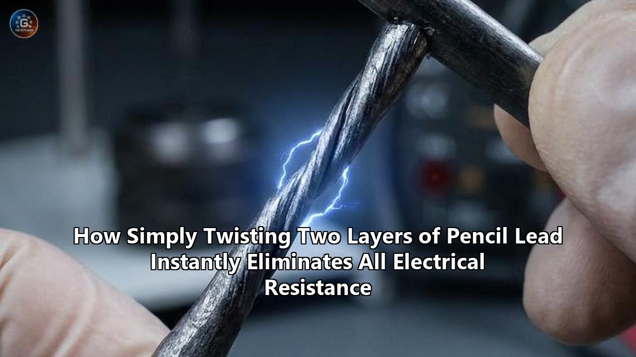
These milestones are bringing a decades-old physics dream closer to reality. By taking two single-atom sheets of carbon—which can be isolated from ordinary graphite, the exact material used in common pencil lead—and rotating one layer by a precise "magic angle" of approximately 1.1 degrees, physicists can instantly eliminate all electrical resistance. This phenomenon represents a massive leap forward in materials science, promising to solve some of the most persistent bottlenecks in modern technology, from the energy-hungry cooling systems of quantum computers to the massive transmission losses in global power grids.
The Global Cost of Friction: Why Electrical Resistance is Our Greatest Invisible Energy Drain
To understand why this discovery has captured the highest honors in science, one must first look at the silent tax paid by every electronic device on Earth: electrical resistance. Whenever an electric current flows through a standard conductor like copper or aluminum, the moving electrons collide with the vibrating atoms of the metal lattice. These collisions act as a form of subatomic friction.
This friction has two major, costly consequences:
- Transmission Waste: Approximately 5% to 10% of all electricity generated worldwide is lost as heat during transmission and distribution. In the United States alone, this equates to billions of dollars of wasted energy annually, requiring power plants to burn more fossil fuels simply to compensate for the power dissipated into the atmosphere.
- Thermal Throttling in Microelectronics: Inside microchips, millions of microscopic copper wires generate localized heat as currents pass through them. This thermal energy limits how tightly transistors can be packed and how fast processors can run without melting. It is the primary reason your laptop gets hot and why hyperscale data centers require gigawatts of electricity solely for cooling.
Conventional Transmission:
[Power Plant] ===(5% to 10% lost as heat due to lattice friction)===> [Home/Factory]

Superconducting Transmission:
[Power Plant] ===(0% lost, 100% current retention at zero resistance)===> [Home/Factory]
Superconductors offer a theoretical escape hatch from this thermodynamic trap. In a superconducting state, electrons pair up to form "Cooper pairs," which flow smoothly through the atomic lattice without any scattering or resistance.
However, since Kamerlingh Onnes first discovered superconductivity in mercury in 1911, the phenomenon has been locked behind a severe thermal barrier. Conventional superconductors require cryogenic cooling down to temperatures near absolute zero—typically below 10 Kelvin (-263 degrees Celsius)—demanding complex and expensive liquid helium systems.
While "high-temperature" cuprate superconductors discovered in the late 1980s can operate at warmer temperatures (above the boiling point of liquid nitrogen, or 77 Kelvin), they are highly brittle, ceramic materials that are notoriously difficult to manufacture, shape into wires, or integrate into microchips. Consequently, the challenge has remained: find a material that is mechanically robust, chemically simple, and capable of displaying highly tunable superconductivity without requiring the extreme environments of outer space.
The Carbon Blueprint: Unlocking Graphene from the Humble Pencil Lead
The path to solving this challenge began with an exceptionally common material: graphite, the soft crystalline form of carbon used to manufacture pencil lead. Graphite consists of countless sheets of carbon atoms stacked on top of one another like sheets of paper in a ream. Within each sheet, the carbon atoms are arranged in a rigid hexagonal honeycomb lattice, bound together by incredibly strong covalent bonds. However, the bonds holding the stacked sheets together—van der Waals forces—are incredibly weak.
When you draw a line with a pencil, the friction against the paper easily shears these weak van der Waals bonds, leaving behind thin stacks of carbon. In 2004, Andre Geim and Konstantin Novoselov at the University of Manchester realized they could exploit this weakness to isolate a single, two-dimensional sheet of carbon atoms. Using ordinary adhesive tape, they repeatedly peeled away layers from a block of graphite until they were left with a single layer. This material, named graphene, earned the duo the 2010 Nobel Prize in Physics.
       Graphite Stack (Pencil Lead)
     ┌───────────────────────────────┐  <- Weak van der Waals forces
     ├───────────────────────────────┤  <- easily sheared by friction
     └───────────────────────────────┘
                     │
                     ▼ (Exfoliation)
             Single-Layer Graphene
              ⬢-⬢-⬢-⬢-⬢-⬢-⬢-⬢-⬢
              | | | | | | | | |
              ⬢-⬢-⬢-⬢-⬢-⬢-⬢-⬢-⬢  <- 2D Honeycomb Carbon Lattice
Graphene proved to be a material of extremes. It is roughly 200 times stronger than steel by weight, highly flexible, and possesses extraordinary thermal and electrical conductivity. In single-layer graphene, electrons behave as "Dirac fermions"—highly mobile particles that move through the carbon lattice as though they have no rest mass, traveling at roughly 1,000 kilometers per second.
Despite these remarkable properties, pristine single-layer graphene is not a superconductor. Because the electrons move so fast and interact so weakly with the atomic lattice, they do not readily pair up. For years, scientists attempted to induce superconductivity in graphene by chemically "doping" it—depositing foreign atoms like calcium or lithium onto its surface to force electron pairing. However, these chemical modifications often degraded graphene's structural integrity and yielded inconsistent results.
The pursuit of pencil lead superconductivity took a major turn when physicists stopped looking at how to modify graphene chemically, and instead started looking at how to stack it geometrically.
The 1.1-Degree Miracle: How Moiré Superlattices Freeze Electrons in Place
The theoretical foundation for this breakthrough was laid in 2011 by Allan MacDonald and Rafi Bistritzer. They calculated that if you took two sheets of graphene, stacked them directly on top of each other, and slowly rotated one layer relative to the other, a massive change would occur in the material's electronic structure.
At a very specific rotational angle—which MacDonald dubbed the "magic angle" of approximately 1.1 degrees—the quantum mechanical waves of the electrons in the two layers would interfere with one another in a way that dramatically slowed down the electrons. In conventional materials, electrons zip through the crystal lattice at breakneck speeds. But at the magic angle, their velocity drops close to zero.
This phenomenon relies on the creation of a "moiré superlattice". When two identical hexagonal lattices are placed on top of one another with a slight rotational offset, they form a new, much larger interference pattern.
Hexagonal Lattice 1:   ⬢ ⬢ ⬢ ⬢ ⬢ ⬢
Hexagonal Lattice 2:   ⬡ ⬡ ⬡ ⬡ ⬡ ⬡  (Rotated by 1.1°)

Moiré Superlattice:    █   ░   █   ░   █   ░
                       (New periodic structure with a 13nm wavelength)
At a 1.1-degree twist, the wavelength of this moiré pattern is roughly 13 nanometers—nearly 50 times larger than the distance between individual carbon atoms in the graphene sheet. This means that a single "super-unit cell" of the moiré pattern contains more than 10,000 carbon atoms.
This giant periodic pattern completely alters how electrons move through the material, giving rise to several key phenomena:
- Band Flattening: In quantum mechanics, the relationship between an electron's energy and its momentum is described by "energy bands." In a single layer of graphene, these bands are highly steep, meaning a small change in momentum results in a massive change in energy, reflecting the high kinetic energy of the electrons. At the 1.1-degree magic angle, these energy bands flatten out completely.
- Quenching of Kinetic Energy: Because the energy band is flat, the kinetic energy of the electrons is suppressed. Electrons that were once racing through the carbon sheets at speeds of thousands of kilometers per second suddenly slow to a crawl, dropping by a factor of 30.
- Dominance of Electron Correlation: When kinetic energy is minimized, the electrostatic repulsion between electrons (Coulomb interaction) becomes the dominant force governing the system's behavior. Instead of ignoring each other as they pass by, the electrons are forced to interact strongly, coordinating their movements to minimize their mutual repulsion.
In 2018, Pablo Jarillo-Herrero's lab at MIT successfully fabricated this structure in a cleanroom, confirming MacDonald's theoretical predictions. When they cooled the magic-angle twisted bilayer graphene (MATBG) down to 1.7 Kelvin, they discovered that by applying an electric voltage to a nearby metal gate, they could tune the material's carrier density. At a specific electron density, the material transitioned from a metal into a "Mott insulator"—a state where electrons are so strongly repelled by each other that they lock in place, refusing to conduct electricity.
Even more remarkably, when they injected slightly more electrons into this insulator, the material underwent a phase transition. The electrons paired up, and the material instantly entered a zero-resistance, superconducting state. This band flattening is the foundational physical engine behind pencil lead superconductivity, proving that geometry alone can induce a quantum phase transition that usually requires complex chemical alloying.
The Twistronics Dilemma: Why 'Magic-Angle' Graphene is Hard to Tame
Despite the initial excitement surrounding Jarillo-Herrero’s 2018 discovery, a massive gap remained between a delicate laboratory demonstration and a practical, scalable technology. The central obstacle in translating pencil lead superconductivity from a liquid-helium-cooled physics curiosity into a commercially viable industrial standard is the extreme, almost absurd level of precision required to fabricate and maintain these twisted structures.
The Precision Problem
The magic angle is not a broad window; it is a razor-thin target centered at 1.1 degrees. If the twist angle between the two graphene sheets deviates by even 0.1 degrees (for example, to 1.0 degrees or 1.2 degrees), the flat energy bands warp, the kinetic energy of the electrons rises, and the superconductivity completely vanishes.
| Twist Angle | Electronic Phase | Physical Behavior |
|---|---|---|
| 0.0° (Aligned) | Semi-metal | Standard bilayer graphene; good conductor but highly resistive under load |
| 0.8° | Strongly correlated metal | Highly resistive; some localized electron interactions, no superconductivity |
| 1.1° (Magic Angle) | Unconventional Superconductor / Insulator | Zero electrical resistance; customizable quantum phases |
| 1.4° | Dispersive metal | Standard conduction; electrons travel too fast to coordinate into Cooper pairs |
To make matters worse, carbon sheets are highly flexible and elastic. When one sheet of graphene is laid down on another, it naturally wants to "slip" back into its lowest-energy thermodynamic state, which is perfectly aligned (0 degrees) or rotated at a high, non-superconducting angle. This tendency is called "structural relaxation" or "self-alignment."
Even if a researcher successfully achieves a 1.1-degree rotation during assembly, the material often develops local wrinkles, bubbles, and rotational "strain" across its surface. This "twist-angle disorder" means that a single flake of graphene might have areas of 1.1 degrees next to areas of 1.05 degrees and 1.15 degrees, resulting in patchy, inconsistent superconductivity that breaks down under current load.
The Problem of Microscopic Exfoliation
The original "Scotch tape" method of isolating graphene is inherently unscalable. It produces tiny, random flakes of single-layer carbon that are often only a few micrometers wide—far too small to be integrated into commercial electronic components or long-distance power lines. Finding these microscopic flakes under an optical microscope, aligning them with sub-degree accuracy using motorized micromanipulators, and transferring them without tearing or folding them remains an incredibly slow, manual process.
The Cryogenic Trap
While the physics of magic-angle twisted bilayer graphene is highly promising, its transition temperature (the critical temperature, $T_c$, below which it becomes a superconductor) is extremely low—typically around 1.7 to 3 Kelvin. This requires cooling the material with liquid helium, which is a scarce, non-renewable resource that is difficult and expensive to manage.
If this material is to be used in real-world quantum computers, sensors, or power transmission lines, scientists must find ways to either raise this critical temperature or develop methods to stabilize and control the superconducting state at higher temperatures.
The Mechanism Mystery
Unlike conventional superconductors, which are well-explained by BCS (Bardeen-Cooper-Schrieffer) theory where lattice vibrations (phonons) glue electrons together, magic-angle graphene is a member of a class known as "unconventional superconductors."
In these materials, the electron pairing is believed to be mediated by direct electronic interactions or quantum geometry. Because physicists did not fully understand how the electrons were pairing up, they lacked a clear roadmap to optimize the material, raise its critical temperature, or manufacture devices with predictable behavior.
The Environmental Lever: Active Control and the Quantum Gating Breakthroughs
Faced with these daunting physical and engineering bottlenecks, the global materials physics community has mobilized. The spring of 2026 has witnessed a series of highly successful solutions targeting the fragile nature of twisted graphene, proving that the material's properties can be stabilized, amplified, and controlled without relying solely on sub-degree structural perfection.
A primary example of this is the breakthrough led by Chun Ning "Jeanie" Lau and her team at Ohio State University, published on May 29, 2026. Rather than focusing solely on perfecting the physical twist angle, Lau's team looked at the surrounding environment of the graphene layers.
They combined twisted bilayer graphene with a synthetic, highly polarizable dielectric substrate: strontium titanate ($\text{SrTiO}_3$), which behaves similarly to a synthetic diamond material under specific electronic conditions.
               [ Top Gate Electrode ]
  ───────────────────────────────────────────────────
              [ Hexagonal Boron Nitride ]
  ===================================================
       [ Twisted Bilayer Graphene (1.1° Twist) ]
  ===================================================
     [ Strontium Titanate (SrTiO3) Substrate ]   <-- High-permittivity dielectric
  ───────────────────────────────────────────────────
              [ Bottom Gate Electrode ]
Strontium titanate possesses an extraordinarily high dielectric constant (permittivity) at cryogenic temperatures. When placed adjacent to the twisted bilayer graphene, it acts as an electrostatic "screen," absorbing and modifying the long-range Coulomb interactions between the electrons in the graphene.
By applying an external voltage to this gate structure, the researchers were able to dynamically change how the electrons interacted with their surroundings. They discovered they could:
- Switch Superconductivity On and Off: By shifting the electrostatic screening of the strontium titanate substrate, they could instantly trigger or collapse the superconducting state without changing the physical twist angle of the carbon sheets.
- Loosen Twist-Angle Tolerance: The screening effect of the substrate helped stabilize the flat energy bands, meaning that even if the twist angle was slightly off (e.g., 1.0 degrees or 1.2 degrees), the material could still be forced into a superconducting state by tuning the external voltage.
- Defy Conventional Physics: The system showed a strong suppression of the typical Coulomb repulsion that normally prevents electron pairing, demonstrating that the environment surrounding a 2D material can be just as influential as the material itself.
This "superconductivity switch" represents a massive leap forward for the design of energy-efficient microchips. If superconductivity can be toggled on and off via simple electrostatic gating, it opens the door to creating superconducting transistors.
Such transistors would generate zero heat when turned "on" (in their superconducting state) and block all current when turned "off" (in their insulating state), eliminating the thermal limits that currently restrict the performance of modern silicon processors.
Complementing this work, the study published in Nature Physics on April 7, 2026, provided a rigorous theoretical and experimental framework for this environmental tuning. Titled "Double-edged role of interactions in superconducting twisted bilayer graphene," the paper explored how changing the electrostatic environment alters the balance between the electron-electron interactions that help superconductivity emerge and the interactions that screen and suppress it.
By showing that local screening can be used as a "dial" to balance these opposing forces, the research team provided physicists with a systematic recipe to optimize pencil lead superconductivity. Instead of treating the material as a rigid, static crystal, scientists can now treat it as an active, tunable quantum laboratory.
Mapping the Superfluid Gap: MIT's Resonator Diagnostics
While the Ohio State University team was mastering the external control of superconductivity, Pablo Jarillo-Herrero's lab at MIT was busy solving the diagnostic challenge: how to peer inside the material and measure exactly how robust its superconducting state is.
In conventional superconductors, the stability of the zero-resistance state is characterized by two fundamental properties:
- Superfluid Stiffness: This refers to the quantum-mechanical rigidity of the superconducting electron pairs. It measures how difficult it is for thermal fluctuations or magnetic fields to disrupt the coordinated flow of the Cooper pairs.
- Superconducting Gap: This is the minimum energy required to break a Cooper pair apart back into individual, resistive electrons. A larger, more resilient gap means the superconductor can operate at higher temperatures and withstand higher currents and magnetic fields before collapsing back into a normal metal.
For years, directly measuring these properties in a 2D material like twisted bilayer graphene was considered nearly impossible because the sample sizes are so small (often less than 10 micrometers across) that traditional bulk measurement techniques are completely useless.
Measuring Superfluid Stiffness
To overcome this obstacle, Jarillo-Herrero’s team collaborated with physicists at Harvard University to develop an entirely new microwave-frequency resonator platform, publishing their results in Nature on February 5, 2025.
They fabricated a highly sensitive superconducting micro-resonator out of aluminum and connected it directly to a flake of magic-angle twisted bilayer graphene. By sending high-frequency microwave signals through the resonator and measuring the tiny changes in the system's "kinetic inductance"—which is directly related to the mass and density of the superconducting Cooper pairs—the team was able to calculate the material's superfluid stiffness for the first time.
                     Microwave Signal In
                             │
                             ▼
  ┌────────────────────────────────────────────────────────┐
  │         Superconducting Aluminum Resonator            │
  └──────────────────────────┬─────────────────────────────┘
                             │ (Probing kinetic inductance)
                             ▼
  ┌────────────────────────────────────────────────────────┐
  │     Magic-Angle Twisted Bilayer Graphene (MATBG)      │
  └────────────────────────────────────────────────────────┘
                             │
                             ▼
                    Microwave Signal Out
          (Tiny phase shifts reveal superfluid stiffness)
The results of this measurement were highly unexpected. The team discovered that the superfluid stiffness in magic-angle graphene is primarily governed by "quantum geometry"—the collective shape of the electronic wavefunctions in the flat band—rather than the speed or density of individual electrons.
This confirmed that the superconductivity in this material is highly unconventional and operates under a completely different set of rules than standard metals. It proved that even though the electrons are slowed to a near-halt, they can still form an incredibly rigid superfluid that flows with zero resistance.
Confirming Unconventional Superconductivity in Trilayer Graphene
Building on this success, on November 6, 2025, Jarillo-Herrero’s team published another seminal paper in Science, focusing on magic-angle twisted tri-layer graphene (MATTG).
In this structure, three sheets of graphene are stacked and twisted relative to each other in a mirror-symmetric "sandwich" configuration (e.g., $+\theta, -\theta, +\theta$). This trilayer structure had previously shown hints of being even more robust than the bilayer version, but direct proof remained elusive.
Using a newly developed "tunneling spectroscopy" platform, the MIT team was able to measure MATTG's superconducting gap directly. The method involved measuring the tunneling current of electrons passing between two isolated layers of twisted graphene as a function of voltage.
They discovered that the superconducting gap in MATTG has a distinct, "V-shaped" or nodal structure. In conventional superconductors, the gap is highly uniform in all directions (known as s-wave pairing). A nodal, V-shaped gap is a definitive hallmark of an unconventional superconductor (such as d-wave pairing, commonly found in high-temperature cuprates).
Conventional Superconductor (s-wave):
   Superconducting Gap Energy
   [██████████████████████████████]  <- Uniform, isotropic gap

Unconventional Superconductor (d-wave/nodal):
   Superconducting Gap Energy
   \            /  \            /
    \    Node  /    \    Node  /
     \    │   /      \    │   /      <- V-shaped, directional nodes
      \───▼──/        \───▼──/
This discovery provides the most direct experimental confirmation to date that magic-angle graphene belongs to the elite family of unconventional superconductors.
Because it exhibits similar physics to cuprate superconductors but consists of nothing but pure carbon, it serves as a pristine, ultra-clean "simulator". Physicists can now use it to study the mysteries of high-temperature superconductivity without the messy structural defects, chemical impurities, and complex crystal lattices of ceramic oxides.
From Two to Three Dimensions: Rhombohedral Graphene and Magnetic Superconductors
As scientists have mastered the art of twisting graphene, they have also begun to explore whether they can achieve similar, zero-resistance quantum states without the mechanical headache of rotation. This has led to another parallel breakthrough: the study of "rhombohedral graphene," which can also be isolated directly from graphite (pencil lead).
In standard graphite, the carbon layers are typically stacked in an alternating "AB-AB-AB" pattern (known as Bernal stacking). However, graphite also contains rare, microscopic regions where the layers stack in a staircase-like "ABC-ABC-ABC" pattern, known as rhombohedral stacking.
Bernal Stacking (AB-AB):      Rhombohedral Stacking (ABC-ABC):
    Layer B:  ○   ○               Layer C:    ●   ●
    Layer A:  ●   ●               Layer B:  ○   ○
    Layer B:  ○   ○               Layer A:  ●   ●
    Layer A:  ●   ●               Layer C:    ●   ●
In late May 2025, a research team at MIT led by Assistant Professor Long Ju published a landmark paper in Nature detailing their work with "pentalayer" rhombohedral graphene—a five-layer stack of carbon atoms isolated from graphite with no twisting whatsoever.
When they cooled this microscopic stack down to 300 millikelvins (just a fraction of a degree above absolute zero) and subjected it to an external electrical field, they observed a spectacular double behavior: the material became both a superconductor and a magnet at the same time.
Historically, magnetism and superconductivity have been considered fundamental enemies. In a classic superconductor, an external magnetic field will quickly destroy the delicate Cooper pairs by forcing their spins to align, collapsing the zero-resistance state (a phenomenon known as the Meissner effect).
However, Long Ju's team discovered that their five-layer rhombohedral graphene was a "chiral superconductor." In this state:
- Coexistence of Order: The material exhibits spontaneous magnetic hysteresis (switching between magnetic states) while remaining completely superconducting with zero electrical resistance.
- High Magnetic Resilience: The critical magnetic field required to destroy the superconductivity was measured at 1.4 Tesla—an exceptionally high value for a material with such a low charge carrier density.
- Spin-Valley Coupling: The electrons in rhombohedral graphene form Cooper pairs where their spins and valley degrees of freedom are locked together, shielding them from the destructive effects of external magnetic fields.
This discovery defies a century of conventional wisdom regarding magnetism and superconductivity. It suggests that the crystalline structures hidden within everyday pencil lead are far more sophisticated than anyone had ever imagined.
By providing a highly stable, non-twisted alternative to bilayer graphene, rhombohedral stacking offers a parallel pathway to developing next-generation quantum devices, such as topologically protected qubits that are immune to external electromagnetic noise.
The Path to Industrialization: From the Lab to the Power Grid
With these spectacular theoretical and experimental breakthroughs established in 2025 and 2026, the scientific community is now shifting its focus from fundamental physics to practical, industrial engineering. If pencil lead superconductivity is to transition from a laboratory bench to our power grids and computers, several key hurdles must be cleared.
1. Scaling Up Graphene Production
The manual "Scotch tape" exfoliation of graphene must be replaced with automated, high-throughput manufacturing methods. The leading candidate is Chemical Vapor Deposition (CVD), a process where carbon-rich gases (such as methane) are decomposed at high temperatures over transition metal catalysts (such as copper or nickel foils) to grow large-area, single-atom sheets of graphene.
CVD Graphene Synthesis:
[Methane Gas (CH4)] ===(Heat 1000°C over Copper Foil catalytic substrate)===> [Continuous Graphene Sheet]
Currently, CVD can produce roll-to-roll sheets of graphene meters in length. However, transferring these sheets onto device substrates, stacking them, and achieving a uniform 1.1-degree twist across large areas remains an incredibly difficult task.
To solve this, advanced nanofabrication facilities are developing "robotic twist-transfer systems." These systems use high-speed optical computer vision and automated micromanipulators to align, rotate, and stamp large-area graphene sheets with millidegree precision, reducing human error and eliminating localized wrinkles and strain.
2. Eliminating the Cryogenic Requirement
While the OSU strontium titanate screening breakthrough has shown that we can make the superconducting state more resilient, the critical temperature ($T_c$) of these materials still hovers below 10 Kelvin. To be commercially viable for power grids, we must raise this temperature.
One highly promising avenue of research involves "strain engineering." By physically stretching or compressing the graphene sheets during the twisting process, scientists can alter the atomic bond lengths and further flatten the electronic energy bands.
Theoretical calculations suggest that combining precise twist angles with targeted biaxial strain could potentially raise the critical temperature of twisted multi-layer graphene into the tens of Kelvin, placing it within the reach of inexpensive, liquid-nitrogen-based cooling systems.
3. Integrating with Silicon Semiconductors
To utilize twisted graphene in consumer electronics, it must be integrated directly into existing silicon fabrication lines (Complementary Metal-Oxide-Semiconductor, or CMOS).
This requires developing low-temperature transfer processes. If graphene is transferred onto silicon wafers at too high a temperature, it can damage the underlying transistors.
Researchers are currently testing sacrificial transfer layers made of polymers that can be dissolved away cleanly, leaving behind pristine, twisted graphene structures directly on top of active silicon circuits.
A Glimpse into the Zero-Resistance Future
The implications of successfully scaling up pencil lead superconductivity are nothing short of civilizational. If this carbon-based technology can be successfully commercialized, it will fundamentally redefine how humanity generates, transmits, and processes energy.
                  ========================================
                  │       THE CARBON-BASED FUTURE        │
                  ========================================
                                     │
         ┌───────────────────────────┼───────────────────────────┐
         ▼                           ▼                           ▼
[ Lossless Power Grids ]     [ Heatless Microchips ]     [ Scalable Quantum Computers ]
- Zero copper losses         - No thermal throttling     - Topologically robust qubits
- High-current capacity      - Ultra-dense processors    - Monolithic integration
- Low infrastructure cost    - Extreme energy savings    - Millisecond coherence times
Lossless Power Transmission
Replacing heavy, resistive copper transmission lines with light, flexible, superconducting graphene cables would instantly recover up to 10% of the world's wasted electricity.
Because carbon is highly abundant and incredibly lightweight compared to copper, these cables would be cheaper to manufacture, easier to string over long distances, and capable of carrying massive currents without overheating. This would make it highly viable to transmit renewable energy from remote solar deserts and offshore wind farms directly to distant metropolitan centers without any loss.
Heatless Supercomputing
Integrating gate-controlled twisted graphene switches into silicon microchips would eliminate the primary physical barrier to computing speed: heat.
Computers could run at clock speeds far exceeding current limits without requiring noisy cooling fans or complex liquid refrigeration.
Data centers, which currently consume more than 2% of the world's electricity (much of it for cooling), would see their power requirements plummet by orders of magnitude, vastly reducing their environmental footprint.
Scalable Quantum Computing
One of the greatest challenges in building practical quantum computers is "decoherence"—the fragile quantum states of qubits are easily destroyed by microscopic thermal and electromagnetic noise.
The discovery of unconventional, robust superconductivity in twisted tri-layer graphene (MATTG) and rhombohedral graphene provides a perfect platform for building "topological qubits."
These qubits would be protected from external noise by the inherent geometry of their wavefunctions, allowing quantum computers to perform complex calculations for minutes rather than microseconds, paving the way for revolutionary advances in medicine, cryptography, and materials design.
What to Watch For Next
As we look forward into the remainder of 2026 and beyond, several critical milestones will signal whether pencil lead superconductivity is successfully transitioning from an academic marvel to an industrial reality:
- Watch for Large-Area CVD Twist-Transfer Demonstrations: Keep an eye out for announcements from nanofabrication companies regarding the automated transfer of 2-inch or 4-inch twisted graphene wafers with uniform angle distribution.
- Monitor the Rising Critical Temperature ($T_c$): Watch for new publications combining twisted graphene with novel substrates or strain engineering to push the superconducting transition temperature above 77 Kelvin.
- Look for Early Prototype Integrations: Watch for partnerships between academic labs (such as MIT, Harvard, or Ohio State) and major semiconductor fabrication companies to build the first hybrid silicon-graphene integrated circuits.
- Follow the Evolution of Twistronics Beyond Carbon: The Kavli Prize-winning principles of twistronics are already being applied to other 2D materials, such as transition metal dichalcogenides (TMDs) and hexagonal boron nitride. These materials may offer even higher transition temperatures and unique electronic phases.
The humble pencil has been a tool of human expression and calculation for centuries. Today, thanks to the prize-winning pioneers of twistronics, it is clear that the very carbon we use to sketch our ideas holds the key to a frictionless, energy-efficient future. By simply twisting two layers of this common material, scientists have unlocked a quantum-mechanical wonderland that will reshape our technological landscape for generations to come.
Reference:
- https://www.chosun.com/english/industry-en/2026/06/10/E56FM7EY3FEYRMHB6KTLHO64XU/
- https://www.sciencedaily.com/releases/2026/05/260528082511.htm
- https://www.grapheneuses.org/nature-physics-highlights-new-graphene-result-superconducting-interactions/
- https://www.bbva.com/en/sustainability/frontiers-award-for-discovering-the-magic-angle-that-unlocks-new-material-properties/
- https://physics.mit.edu/news/mit-physicists-turn-pencil-lead-into-gold/
- https://news.mit.edu/2025/physicists-measure-key-aspect-superconductivity-magic-angle-graphene-0205
- https://thevarsity.ca/2017/02/12/your-pencil-is-now-a-superconductor/
- https://www.youtube.com/watch?v=s4QmHApzOQc
- https://news.mit.edu/2025/physicists-observe-evidence-unconventional-superconductivity-graphene-1106
- https://www.sciencenews.org/article/twisted-carbon-graphene-superconductor
- https://www.impactlab.com/2025/02/20/mit-breakthrough-measures-superfluid-stiffness-in-magic-angle-graphene-paving-the-way-for-quantum-computing/
- https://scitechdaily.com/mit-discovers-magnetic-superconductor-in-pencil-lead/
- https://scienceblog.com/mit-discovers-magnetic-superconductor-in-pencil-lead/
- https://www.cloudynights.com/forums/topic/966715-mit-scientists-turn-pencil-lead-into-a-magnetic-superconductor/