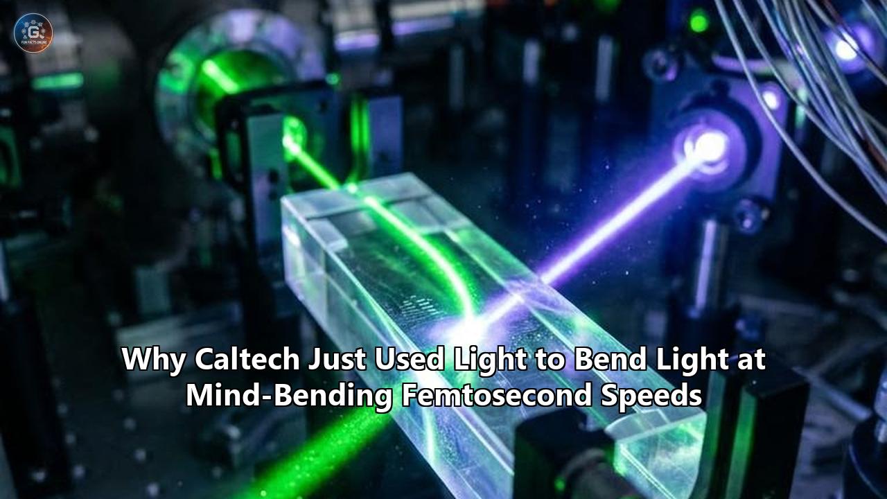
In an era where electronic microprocessors are pushing up against the hard physical limits of thermodynamics and silicon clock speeds, researchers at the California Institute of Technology (Caltech) have achieved a milestone in ultrafast optics. In a study published in Nature Nanotechnology, a team led by Professor Harry Atwater demonstrated an all-optical chip capable of using one beam of light to steer another beam across angles of up to ±13 degrees in just 74 femtoseconds.
To put that timeframe into perspective, 74 femtoseconds—74 quadrillionths of a second—is roughly the time it takes a pulse of light to travel across the width of a single human hair.
The breakthrough overcomes a fundamental hurdle in physics: photons, unlike electrons, carry no electrical charge and generally pass straight through one another without interacting. By engineering an ultrathin metasurface made of nanoscale silicon pillars, the Caltech team amplified the extremely weak interactions between photons. The result is a system where a high-intensity "pump" laser alters the local optical properties of a material on demand, redirecting a secondary "probe" laser almost instantaneously.
"Steering light with light is very challenging because light typically interacts very weakly with matter," said Harry Atwater, the Howard Hughes Professor of Applied Physics and Materials Science at Caltech. "Using optical metasurfaces—ultrathin, carefully nanoengineered sheets—we can up the interaction strength to make this possible with much higher efficiency."
The lead author of the study, Claudio Hail, conducted the experiments as a postdoctoral scholar in Atwater’s laboratory before joining the faculty at the University of California, Berkeley. Hail noted that the operational speed of the device was strictly limited by the pulse duration of the driving laser itself—meaning that with even shorter laser pulses, the response time could become even faster.
This achievement marks a major leap toward all-optical computing, ultra-high-bandwidth wireless communications, and solid-state beam-steering systems that operate without moving mechanical parts or electronic switching bottlenecks.
The Fundamental Problem: Photons Don't Like to Talk to Each Other
To understand why this achievement is significant, it helps to examine how modern information infrastructure processes data. Today’s internet runs on light traveling through fiber-optic cables over long distances. Light possesses virtually unmatched bandwidth and moves at the ultimate speed limit of the universe. However, whenever a data packet reaches a network router or a computing node, that optical signal must be converted into an electrical signal, processed by silicon transistors, and converted back into light.
This optical-to-electronic-to-optical (O-E-O) conversion creates a major speed bump. Electronic transistors process information by physically moving electrons through semiconductors. This process generates substantial heat, consumes energy, and suffers from capacitive delays that have kept microchip clock speeds hovering around 3 to 5 gigahertz (GHz) for nearly two decades.
Photons offer a solution. If computing chips could route, switch, and process data using light instead of electricity, processing speeds could reach the terahertz (THz) or petahertz (PHz) regime while consuming a fraction of the energy.
TRADITIONAL OPTICAL ROUTING (O-E-O Bottleneck):
[Optical Signal] ---> [Photodetector] ---> [Electrical Transistor] ---> [Laser Diode] ---> [Optical Signal]
                                                  |
                                      (Heat & Bandwidth Delay)

ALL-OPTICAL ROUTING (Caltech Approach):
[Optical Signal] ------------------------------------------------------------------------> [Redirected Optical Signal]
                                        ^
                                        |  (74-femtosecond deflection)
                               [Light Control Beam]
However, building an all-optical circuit requires a mechanism for light bending light—meaning one light signal must directly dictate the path, phase, or intensity of another. In standard classical optics governed by linear electromagnetism, photons obey the principle of superposition. When two light beams cross path in open air or in standard glass, they pass straight through each other unchanged. To force photons to interact, they must be brought together inside a non-linear material medium.
For decades, attempts to create light-controlled optical switches have run into a fundamental trade-off between speed and efficiency:
- Resonant Electronic Carrier Excitation: Traditional optoelectronic switches hit a material with light to excite real electrons across a semiconductor's bandgap, pushing them into higher energy states. This creates large shifts in the material’s index of refraction, making it easy to steer light. But those excited electrons must eventually decay back down to their ground state. This "carrier relaxation" process takes picoseconds to nanoseconds, imposing a hard upper limit on how fast the system can reset.
- Non-Resonant Ultrafast Nonlinearities: Alternatively, light can interact with a material instantaneously through nonlinear optical polarization. However, these non-resonant effects are exceptionally weak. Achieving meaningful light deflection historically required gigantic high-power lasers or long propagation distances through kilometers of specialized fiber optic cables.
The Caltech team bypassed this trade-off by engineering a nanostructure that magnifies weak instantaneous light interactions without triggering slow electronic delays.
Deconstructing the Physics: The Optical Kerr Effect
At the heart of the Caltech device lies a quantum phenomenon known as the Optical Kerr Effect.
The optical Kerr effect is a third-order non-linear optical process ($\chi^{(3)}$ nonlinearity) in which an intense electric field of light modifies a material's refractive index ($n$), which determines how fast light propagates through that medium. Mathematically, the refractive index under the Kerr effect is expressed as:
$$n(I) = n_0 + n_2 I$$
Where:
- $n_0$ is the linear refractive index of the material at low light intensities.
- $n_2$ is the non-linear refractive index coefficient.
- $I$ is the optical intensity of the light passing through.
When an intense laser pulse—the "pump" beam—strikes a Kerr-nonlinear medium, its strong electric field exerts a force on the bound electrons surrounding the atomic nuclei. Crucially, this force does not kick the electrons up into higher, unoccupied energy bands. Instead, it slightly distorts the shape of their electron orbitals.
ELECTRON DYNAMICS IN OPTICAL MODULATION:

1. Traditional Excitation (Slow: Picoseconds to Nanoseconds)
   [Conduction Band]  <--- Electron Excited (Absorbs Energy)
         ^                                |
         | (Band Gap Energy)              v (Relaxation Delay)
   [Valence Band]     ---------------------

2. Optical Kerr Effect (Ultrafast: Sub-Femtosecond)
   [Bound Orbital]    <--- Orbital Distorted by Light's Electric Field
                      <--- Returns to Normal Instantly as Light Leaves
Because the electrons are never boosted into separate, long-lived energy states, they do not need to undergo a slow relaxation process. As soon as the laser pulse passes, the atomic electron clouds snap back to their original shapes instantaneously. The intrinsic response time of this Kerr polarization is sub-femtosecond.
The practical problem has always been the value of $n_2$. In conventional dielectric materials like fused silica or silicon, $n_2$ is tiny—typically on the order of $10^{-14}$ to $10^{-18} \text{ cm}^2/\text{W}$. To alter the refractive index enough to bend an intersecting beam of light, one would normally need to blast the material with gigawatt-level laser pulses, which risks melting the device.
The Metasurface Architecture: Trapping Light in Nanoscale Pillars
To make the optical Kerr effect practical at low power, Atwater and Hail turned to the field of flat optics and nanophotonics. They fabricated a custom metasurface—an engineered 2D sheet covered with subwavelength microscopic structures called "meta-atoms".
METASURFACE CROSS-SECTION (Conceptual Representation):

       Incident Pump Beam                 Incident Probe Beam
              |                                   |
              v                                   v
  +---------------------------------------------------+
  |   |||   |||   |||   |||   |||   |||   |||   |||   | <-- Amorphous Silicon Nanopillars
  |   |||   |||   |||   |||   |||   |||   |||   |||   |     (High-Q Resonators)
  +---------------------------------------------------+
  |                  Quartz Substrate                 |
  +---------------------------------------------------+
                                  \
                                   \ Deflected Probe Beam (Steered up to 13°)
                                    v
The device consists of an ultrathin array of nanoscale pillars made from amorphous silicon sitting on a glass substrate. Each individual pillar is smaller than the wavelength of light it interacts with.
The key to the design lies in configuring the nanopillars to exhibit a high Quality Factor (high-Q) optical resonance.
When light strikes a standard flat piece of glass, it passes through in a straight line almost instantly. In contrast, when light hits Caltech’s high-Q metasurface, the individual silicon nanopillars act as tiny optical cavity traps. The incoming photons bounce inside the nanopillars for a few optical cycles before being re-emitted.
This brief light-trapping effect yields two crucial outcomes:
- Field Concentration: Trapping the light inside a subwavelength volume boosts the local electric field intensity inside the silicon by orders of magnitude. Because the refractive index change $\Delta n = n_2 I$ depends directly on intensity ($I$), boosting the field amplifies the strength of the optical Kerr effect without requiring more laser power.
- No Slow Carrier Bottleneck: Unlike plasmonic metasurfaces made of metals (which generate high heat and optical loss) or semiconductor systems that rely on free-carrier absorption, the high-Q dielectric silicon structures trap light while maintaining non-resonant Kerr interactions.
How the Steering Mechanism Works
To steer a beam of light using another beam, the team used a dual-beam setup: a spatially structured pump beam and a weaker probe beam.
- Projection: The intense pump laser pulse is projected onto the metasurface with a spatially varying intensity pattern (for instance, a linear intensity ramp across the surface).
- Modulation: Where the pump beam is brightest, the optical Kerr effect alters the refractive index of the silicon nanopillars the most. Where the pump beam is dim, the refractive index changes very little. This creates a temporary gradient-index prism across the chip.
- Deflection: Simultaneously, the probe beam arrives at the metasurface. As it passes through this light-induced gradient, the optical phase of the wavefront shifts unequally across the surface, causing the entire probe beam to bend sideways by up to 13 degrees.
- Reset: The moment the 74-femtosecond pump pulse terminates, the electron orbitals snap back, the artificial prism vanishes, and the device resets.
HOW THE PUMP PATTERN BENDS THE PROBE BEAM:

Pump Intensity Pattern:  [ Low Intensity  ------------>  High Intensity ]
Refractive Index Shift:  [ Small Δn       ------------>  Large Δn       ]
Phase Delay Across Chip: [ Minimal Delay  ------------>  Maximum Delay  ]
                                       |
                                       v
Resulting Wavefront:     /  /  /  /  /  (Tilted Wavefront = Steered Light)
By altering the spatial pattern of the pump beam, the researchers demonstrated that they could dynamically control the angle and direction of the redirected probe beam in real time.
Experimental Performance Breakdown
The table below outlines the core metrics demonstrated by the Caltech researchers in their published experiment:
| Parameter | Caltech Experimental Value | Conventional Optoelectronic Devices | Impact / Significance |
|---|---|---|---|
| Response Time | 74 femtoseconds ($7.4 \times 10^{-14} \text{ s}$) | 1 picosecond to 10 nanoseconds | Over 100 to 10,000 times faster than existing electro-optic switches. |
| Steering Deflection Angle | Up to $\pm 13^\circ$ in near-infrared | $1^\circ - 5^\circ$ (for traditional static metasurfaces) | Wide deflection angle enables practical optical signal routing. |
| Primary Physics Mechanism | Non-resonant Optical Kerr Effect | Interband/Intraband free-carrier absorption | Eliminates recombination delays, enabling pulse-limited operation. |
| Metasurface Material | High-Q Amorphous Silicon | Metals (Plasmonic) or Lithium Niobate | Low optical loss, high non-linear index, CMOS manufacturing compatible. |
| Control Signal Source | Spatially structured laser pulse (Pump) | Electrical current/voltage | Direct light-by-light manipulation with zero electronic interface. |
A notable takeaway from the experiment was that the 74-femtosecond modulation speed was limited by the pump laser pulse itself, not by the metasurface material.
"The researchers note that the current modulation speed is still set by the duration of the laser pulses that drive the system rather than by the metamaterial's intrinsic properties," Caltech noted in an official statement. If driven by a 10-femtosecond laser, the metasurface could theoretically re-route light on an even shorter scale.
Real-World Applications: Why All-Optical Beam Steering Matters
Achieving ultrafast spatial light control opens up possibilities across multiple high-tech industries.
                  +----------------------------------------------+
                  |  ULTRAFAST LIGHT-BY-LIGHT BEAM CONTROL       |
                  +----------------------------------------------+
                                         |
         +-------------------------------+-------------------------------+
         |                               |                               |
         v                               v                               v
+------------------+           +-------------------+           +-------------------+
| Optical AI &     |           | Ultra-Wideband    |           | Solid-State       |
| Quantum Computing|           | Telecom & Li-Fi   |           | Femtosecond LiDAR |
+------------------+           +-------------------+           +-------------------+
| Multi-terahertz  |           | Free-space optical|           | Instantaneous     |
| optical switches |           | data routing      |           | 3D scanning       |
| replace silicon  |           | without O-E-O     |           | with no moving    |
| transistors|         | bottleneck        |           | mechanical parts  |
+------------------+           +-------------------+           +-------------------+
1. Multi-Terahertz All-Optical Computing and AI Acceleration
Modern artificial intelligence models require massive matrix-vector multiplications. Electronic graphics processing units (GPUs) consume immense power pushing billions of bits through metallic interconnects, generating heat and encountering RC latency bottlenecks.
By replacing electronic logic gates with optical switches that operate via light bending light, future processors could compute at optical frequencies. Photonic integrated circuits (PICs) using metasurface routing could perform complex computations in a single pass of light through a chip at clock rates exceeding 10 terahertz—thousands of times faster than today's 5 GHz processors—with minimal heat generation.
2. Next-Generation Telecommunications and Free-Space Li-Fi
As world data traffic explodes, fiber optic networks and wireless communications are approaching capacity limits. Current telecommunication nodes use electro-optic modulators to direct signals.
Ultrafast spatial light modulators operating at femtosecond speeds could enable instantaneous spatial division multiplexing. Light signals carrying terabytes of data could be switched between different optical fibers or redirected through free space (Li-Fi) without ever being converted to electricity, drastically decreasing internet infrastructure latency and energy consumption.
3. Solid-State LiDAR for Autonomous Vehicles and Robotics
Light Detection and Ranging (LiDAR) systems emit laser pulses to map physical environments in 3D. Today's commercial LiDARs rely on mechanical spinning mirrors or slow micro-electro-mechanical systems (MEMS) to sweep the laser beam across a field of view. These mechanical parts are susceptible to wear, vibration, and mechanical failure.
While electronic optical phased arrays (OPAs) exist, they are often limited in steering speed and angular resolution. A metasurface powered by optical Kerr switching can steer beams across wide angles at sub-picosecond speeds without any moving parts, paving the way for compact, fully solid-state LiDAR sensors that fit onto a tiny chip.
Comparing Ultrafast Optical Technologies
To place Caltech's breakthrough in perspective, it helps to compare it against other state-of-the-art approaches in ultrafast photonics.
COMPARING ULTRAFAST PHOTONIC PLATFORMS:

[ Plasmonic Metasurfaces ]  ---> Fast, but high optical loss (Metals absorb light)
[ Thin-Film Lithium Niobate]---> Strong electro-optic effect, but relies on electronic drive voltages
[ Transparent Oxides (ITO) ] ---> High index change, but limited by slow free-carrier decay
[ Caltech Silicon Kerr Metasurface ] ---> Ultrafast (74 fs), low loss, pure light-by-light control
Thin-Film Lithium Niobate ($\text{LiNbO}_3$) Nanophotonics
Lithium niobate is a foundational material in modern telecommunications due to its strong Pockels effect (a second-order $\chi^{(2)}$ electro-optic nonlinearity). Platforms developed at institutions like Caltech (in Alireza Marandi's laboratory) and Harvard have produced integrated optical switches and frequency combs.
However, conventional Pockels-effect devices require an external electrical voltage applied via metallic electrodes to induce an index change. This electrical interface introduces capacitive RC delays and high driver-power requirements at ultra-high frequencies. Caltech's Kerr metasurface operates purely all-optically, eliminating metal electrodes entirely.
Plasmonic Metasurfaces
Plasmonic devices utilize surface plasmon polaritons—coupled oscillations of light and free electrons at metal-dielectric interfaces—to squeeze light into sub-nanometer volumes. While plasmonic structures produce strong light-matter interactions, metals like gold and silver suffer from intrinsic ohmic absorption losses. Much of the optical energy is lost as heat.
Caltech's low-loss dielectric approach uses amorphous silicon, which preserves optical power while maintaining high field concentration.
Transparent Conducting Oxides (TCOs)
Materials such as Indium Tin Oxide (ITO) and Aluminum-doped Zinc Oxide (AZO) exhibit extremely large refractive index changes in their "Epsilon-Near-Zero" (ENZ) spectral regions. However, these changes rely heavily on intraband free-carrier excitation. Electrons are driven into higher energy states within the conduction band, causing a relaxation delay of several picoseconds before the material resets.
The non-resonant Kerr mechanism used by Hail and Atwater avoids free-carrier excitation, allowing for sub-picosecond reset times.
Engineering Challenges and the Path to Commercialization
While steering a laser beam in 74 femtoseconds is a scientific milestone, translating this laboratory breakthrough into commercial technologies will require solving several engineering challenges.
ENGINEERING ROADMAP TO COMMERCIALIZATION:

[ Lab Prototype ] ------------> [ Integrated Lasers ] ----------> [ Mass Manufacturing ]
* Tabletop femtosecond laser    * Microcomb / Mode-locked        * Deep-UV lithography on 300mm
* 74 fs response demonstrated     lasers integrated on-chip        silicon wafers
* Precise pump profiling        * Low power consumption          * Packaging with PIC fiber networks
1. On-Chip Integration of Femtosecond Laser Sources
In the laboratory demonstration, the pump pulses were generated by a benchtop femtosecond laser system. For this technology to work inside a smartphone, datacenters, or autonomous cars, engineers must integrate femtosecond pulse generators directly onto microchips.
Advancements in Kerr microcombs and integrated mode-locked lasers on silicon photonic platforms are progressing rapidly, but miniaturizing high-peak-power pulse sources remains an active area of research.
2. Mitigating Two-Photon Absorption (TPA)
Although the experiment relied primarily on the non-resonant Kerr effect, high optical intensities in semiconductors can occasionally trigger Two-Photon Absorption (TPA). TPA occurs when an electron simultaneously absorbs two photons, jumping across the bandgap and creating free electrons.
In their paper, the authors noted a minor background contribution from two-photon-excited free carriers. At extremely high repetition rates (tens of gigahertz), residual free carriers could accumulate, generating heat and slowing the recovery time. Materials with wider optical bandgaps—such as silicon nitride ($\text{Si}_3\text{N}_4$) or titanium dioxide ($\text{TiO}_2$)—are being explored to completely suppress TPA.
3. Scalable Nanofabrication
Fabricating arrays of subwavelength silicon nanopillars requires high-precision nanolithography. While electron-beam (E-beam) lithography is ideal for prototyping in research environments, commercial scaling will rely on deep-ultraviolet (DUV) or extreme-ultraviolet (EUV) photolithography lines currently used by semiconductor foundries. Ensuring uniform feature sizes across a multi-inch wafer is critical to maintaining uniform optical resonance.
What to Watch For Next
The demonstration of pulse-limited light bending light in 74 femtoseconds marks a shift in how engineers approach optical signal processing. Moving forward, several key milestones will signal the transition of this technology from fundamental physics to real-world deployment:
- Sub-10-Femtosecond Switching: Researchers plan to drive these high-Q metasurfaces with even shorter, few-cycle laser pulses to test the ultimate physical speed limit of Kerr-driven beam manipulation.
- Two-Dimensional Arbitrary Wavefront Shaping: Demonstrating full 2D dynamic spatial light modulation, where light patterns can be reconfigured into arbitrary shapes, holograms, or multi-beam splitters on femtosecond timescales.
- Monolithic Photonic Integration: Combining Kerr metasurfaces directly with silicon waveguides, photodetectors, and on-chip microcomb lasers to build completely self-contained all-optical processing engines.
- Quantum Information Processing: Applying ultrafast spatial control to entangled single-photon states, laying the foundation for high-speed quantum routers and optical quantum computers.
By demonstrating that light can control and bend light at speeds governed strictly by the duration of the light pulse itself, the Caltech team has provided a blueprint for bypassing the electronic speed limit. As optical metasurface engineering continues to converge with semiconductor manufacturing, the dream of ultra-fast, all-optical computing and high-bandwidth photonics moves closer to reality.
References & Further Reading
- Primary Study: Hail, C., et al. (2026). Pulse-limited spatial light modulation and beam steering in high-Q non-linear metasurfaces. Nature Nanotechnology.
- Caltech Division of Engineering and Applied Science: Research updates from the Harry Atwater Laboratory (Thomas J. Watson Laboratory of Applied Physics).
- Related Research: Sekine, R., Marandi, A., et al. (2025). Ultra-broadband lithium niobate nanophotonic optical parametric oscillators. Nature Photonics.
- Metasurface Fundamentals: Shirmanesh, G. K., & Atwater, H. A. (2021). Electro-Optically Tunable Metasurfaces for Comprehensive Control of Light. Caltech Doctoral Thesis.
Reference:
- https://www.caltech.edu/about/news/steering-light-in-a-flash-new-chip-redirects-light-beams-in-less-than-a-trillionth-of-a-second
- https://pubmed.ncbi.nlm.nih.gov/42332252/
- https://scitechdaily.com/caltechs-new-device-steers-light-with-light-at-mind-bending-speed/
- https://thesis.caltech.edu/16983/01/Li_Gordon_2025.pdf
- https://thesis.caltech.edu/13955/
- https://www.caltech.edu/about/news/new-optical-switch-could-lead-to-ultrafast-all-optical-signal-processing
- https://knowridge.com/2026/07/scientists-create-ultra-fast-chip-that-redirects-light-in-less-than-a-trillionth-of-a-second/
- https://www.caltech.edu/about/news/nanoscale-device-simultaneously-steers-and-shifts-frequency-of-optical-light-pointing-the-way-to-future-wireless-communication-channels
- https://www.admissions.caltech.edu/explore-more/news/bending-light-tiny-chip-42252
- https://www.electrooptics.com/news/caltech-researchers-create-light-projecting-silicon-chip
- https://www.caltech.edu/about/news/uniting-the-light-spectrum-on-a-chip
- https://light.caltech.edu/
- https://scitechdaily.com/revolutionizing-light-control-caltechs-mind-bending-3d-printed-optical-devices/