For more than two decades, materials scientists and solid-state physicists treated wrinkles in two-dimensional sheets as a manufacturing defect—an irritating byproduct of chemical vapor deposition and transfer processes that degraded electron mobility and ruined device uniformity. In cleanrooms from Silicon Valley to Hsinchu, process engineers spent millions of dollars trying to flatten graphene to preserve its pristine, planar honeycomb lattice.
That foundational assumption has now been upended.
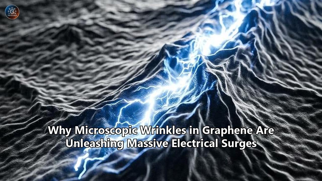
A multinational research collaboration led by Rice University, working alongside teams from the University of Manchester, the University of Brighton, the South Dakota School of Mines and Technology, the University of Sussex, and Pennsylvania State University, has proven that microscopic, sub-nanometer wrinkles in graphene act as powerful electronic engines. Published in Advanced Materials, the study demonstrates that when graphene buckles into creases whose radius of curvature approaches atomic dimensions—less than a single nanometer across—the local material generates an electrical polarization between 100,000 and 10 million times stronger than that observed in conventional bulk flexoelectric materials.
When biased with a modest potential of approximately one volt, these microscopic ripples do not merely impede charge; they channel and unleash localized electrical current surges.
The finding delivers the first direct experimental validation of "quantum orbital flexoelectricity" in 2D systems, a theoretical concept first proposed nearly two decades ago. More critically, it reveals that structural geometry alone can serve as an electronic control knob, bypassing the chemical dopants, electrostatic gating layers, and complex lithographic patterning that have historically constrained two-dimensional semiconductor design.
        Planar Graphene                          Wrinkled Graphene (Sub-nm Curvature)

    (Uniform π-orbitals)                 (Orbital Distortion & Inversion Symmetry Breaking)
        o---o---o---o                                    .-"-.  <-- Convex: π-lobes expand outward
       / \ / \ / \ / \                                  /  •  \     Partial sp²-to-sp³ rehybridization
      o---o---o---o---o                                |   •   |
       \ / \ / \ / \ /                                 |   •   |
        o---o---o---o                                 /         \
                                                     o           o  <-- Concave: σ-bonds compressed
  • Charge Distribution: Symmetrical             --------------------------------------------------
  • Net Dipole Moment: Zero                      • Flexoelectric Polarization: 10⁵–10⁷× bulk
  • Local Gauge Field: Zero                      • Gauge Field: Pseudomagnetic fields (>100 T)
                                                 • Work Function: Abrupt local potential drop (ΔΦ)
                                                 • Transport: Directional carrier channeling & surges
The 18-Year Theoretical Cold Case in Nanophysics
To understand why this discovery took the condensed matter physics community by surprise, one must look back to 2008. Theoretical physicist Vincent Meunier—then at Oak Ridge National Laboratory and now the P. B. "Pete" Brenan Chair of Physics and Materials Science and Engineering at Rice University—alongside physicist Sergei Kalinin, published calculations indicating that extreme, non-uniform mechanical bending in carbon networks would warp the local electronic wavefunctions.
In a perfectly planar graphene crystal, carbon atoms form three in-plane $\sigma$-bonds via $sp^2$ hybridization, arranged at $120^\circ$ angles, while the remaining $p_z$ orbitals extend perpendicularly above and below the atomic sheet. These unhybridized $p_z$ orbitals form a delocalized $\pi$-electron cloud that spreads symmetrically across the top and bottom faces of the crystal. Because the crystal structure possesses inversion symmetry, planar graphene is non-polar; it cannot exhibit spontaneous electrical polarization, nor can it display classical piezoelectricity—the generation of an internal electric field under uniform mechanical stress.
Meunier and Kalinin calculated that if one could bend the carbon sheet tightly enough, the mechanical strain gradient across the atomic monolayer would break this symmetry. The $p_z$ orbitals on the convex (outer) side of the curve would be forced to spread apart, while the orbital lobes on the concave (inner) side would be squeezed together. This asymmetry would force the out-of-plane $\pi$-orbitals to mix with the underlying in-plane $\sigma$-orbitals—a phenomenon known as quantum flexoelectricity or electronic flexoelectricity.
                  UNSTRAINED                                 CURVED (SUB-NANOMETER)
             Planar sp² Hybridization                      Quantum Orbital Mixing

                 (π-orbital lobe)                                (Expanded π-lobe)
                     +-----+                                          +-------+
                     |     |                                         /         \
                 ---[ Carbon ]---                                ---[  Carbon   ]---
                     |     |                                         \         /
                     +-----+                                          +-------+
                 (π-orbital lobe)                                (Compressed π-lobe)

           • Symmetrical distribution                     • Asymmetrical charge distribution
           • Inversion symmetry preserved                 • Inversion symmetry broken
           • Net dipole = 0                               • Local dipole moment (P_flexo ≠ 0)
The resulting charge shift would create a permanent, localized electric dipole moment aligned along the axis of curvature. The smaller the radius of curvature, the steeper the strain gradient, and the more intense the resulting electric polarization would become.
For nearly twenty years, however, Meunier’s prediction remained a theoretical curiosity. Experimentalists who tried to measure the phenomenon ran into an intractable metrological barrier: atomic force microscopy (AFM). To bend graphene in a laboratory, researchers routinely pressed sharp diamond or silicon tips into suspended membranes. But the physical force of the AFM tip introduced external contact stresses, tip-sample electrostatic artifacts, and substrate-induced charges that swamped the subtle quantum signals they were trying to detect.
Moreover, mechanically manipulating graphene via cantilever tips produced broad, gentle ripples with radii of curvature measuring tens or hundreds of nanometers. At those macroscopic scales, the strain gradient was simply too weak to induce observable orbital rehybridization.
The breakthrough occurred when Sathvik Ajay Iyengar, then a doctoral researcher working in the laboratory of materials scientist Pulickel M. Ajayan at Rice University, began re-examining anomalous scanning probe datasets collected with collaborator Manoj Tripathi.
Rather than artificially deforming graphene with mechanical probes, the team investigated self-assembled graphene sheets grown on molybdenum disulfide ($\text{MoS}_2$) substrates. Because graphene and $\text{MoS}_2$ possess fundamentally different crystal lattice constants and thermal expansion coefficients, the graphene layer naturally buckles as it cools down from the high growth temperatures of chemical vapor deposition.
As the graphene contracts against the rigid underlying crystal, it relieves mechanical stress by crumpling into a dense array of self-assembled nanowrinkles.
When Iyengar and the team mapped these naturally occurring ridges, they discovered that the bends were confined to sub-nanometer dimensions. The apex of each wrinkle had a radius of curvature on the order of 0.5 nanometers—roughly five angstroms, or the width of just a few carbon rings. The curvature reached an astounding $10^9\text{ m}^{-1}$, three orders of magnitude sharper than any deformation previously analyzed in experimental flexoelectric literature.
When the researchers brought conductive microscopic probes near these sub-nanometer apexes without pressing down on them, the data showed intense, localized electrical anomalies. The theoretical cold case was cracked: the sharpest wrinkles were acting like tiny, self-contained electric power plants, generating local charge separations and sparking electrical current surges under low driving voltages.
Orbital Mechanics and the Mathematics of Curvature
To grasp how these nanoscale deformations reshape graphene electrical properties, one must examine the electronic Hamiltonian of a carbon lattice under inhomogeneous strain gradients.
In undisturbed graphene, electrons occupy states described by the massless Dirac equation, where the energy dispersion relation is strictly linear near the corners of the first Brillouin zone—the Dirac points ($K$ and $K'$):
$$E(\mathbf{k}) = \pm \hbar v_F |\mathbf{k} - \mathbf{K}|$$
Here, $v_F \approx 10^6\text{ m/s}$ represents the Fermi velocity, $\hbar$ is the reduced Planck constant, and $\mathbf{k}$ is the wavevector. The density of states at the Dirac point drops to zero, rendering pristine graphene a zero-bandgap semimetal.
       PRISTINE GRAPHENE (Dirac Cone)              WRINKLED GRAPHENE (Gauge Field Shift)

                    E                                           E
                    |                                           |
                   / \                                         / \
                  /   \                                       /   \
                 /  *  \                                     /  *  \
                / /   \ \                                   / /   \ \
               / /     \ \                                 / /     \ \
  ------------*-----------*------------       ------------*-----------*------------
             K             K'                            K             K'

         • E(k) = ± ħ v_F |k - K|                 • E(k) = ± ħ v_F |k - K - eA/ħ|
         • Symmetric, Zero Gap                    • Asymmetric Hopping (t_ij ≠ t_0)
         • No Gauge Field (A = 0)                 • Gauge Field: B_pseudo = ∇ × A > 100 T
                                                  • Bandgap Opening: ΔE_g ~ 100–300 meV
When a graphene sheet is bent into a sub-nanometer ridge, this pristine electronic environment collapses. The mechanical deformation introduces an inhomogeneous strain tensor, $\varepsilon_{ij}(\mathbf{r})$, where the strain varies continuously as a function of the spatial coordinate across the wrinkle:
$$\varepsilon_{ij} = \frac{1}{2} \left( \frac{\partial u_i}{\partial x_j} + \frac{\partial u_j}{\partial x_i} + \frac{\partial h}{\partial x_i}\frac{\partial h}{\partial x_j} \right)$$
where $u_i$ represents the in-plane displacement field and $h(\mathbf{r})$ represents the out-of-plane out-of-plane topography (the wrinkle height profile).
Because the radius of curvature $R$ drops to $\sim 0.5\text{ nm}$, the carbon-carbon bond lengths ($a_0 \approx 0.142\text{ nm}$) at the crest of the wrinkle are stretched by more than $10\%$ on the outer surface while simultaneously being compressed along the inner basal plane.
This extreme distortion alters the nearest-neighbor electronic hopping amplitudes, $t_{ij}$, which govern how easily an electron can tunnel from one carbon atom to the next. In planar graphene, all three nearest-neighbor hopping integrals are identical ($t_1 = t_2 = t_3 \approx 2.8\text{ eV}$). Under sub-nanometer curvature, the hopping integrals become directionally anisotropic:
$$t_{ij} = t_0 \exp\left[ -\beta \left( \frac{d_{ij}}{a_0} - 1 \right) \right]$$
where $\beta \approx 3.37$ is the electron-phonon coupling parameter, and $d_{ij}$ is the modified bond distance between adjacent carbon atoms.
This modification acts on the Dirac electrons as an effective vector gauge potential, $\mathbf{A} = (A_x, A_y)$, defined by:
$$A_x = \frac{\hbar \beta}{2 e a_0} (\varepsilon_{xx} - \varepsilon_{yy})$$
$$A_y = -\frac{\hbar \beta}{e a_0} \varepsilon_{xy}$$
The modified Dirac Hamiltonian under this strain field becomes:
$$\mathcal{H} = v_F \boldsymbol{\sigma} \cdot \left( \mathbf{p} - e\mathbf{A} \right) + V_{\text{flexo}}(\mathbf{r})$$
The curl of this vector potential creates an artificial, or "pseudo-magnetic," field:
$$\mathbf{B}_{\text{pseudo}} = \boldsymbol{\nabla} \times \mathbf{A}$$
Because the strain changes drastically over a sub-nanometer distance, the spatial gradient $\boldsymbol{\nabla} \times \mathbf{A}$ reaches massive proportions.
Inside the crest of these nanowrinkles, the induced pseudomagnetic field exceeds 100 to 300 Tesla—far surpassing the highest continuous magnetic fields ever generated in national high-field magnet laboratories (which top out around 45 Tesla for continuous hybrid magnets).
Crucially, this pseudomagnetic field does not break global time-reversal symmetry because it assumes opposite signs at the two distinct valleys ($+B_{\text{pseudo}}$ at the $K$ valley and $-B_{\text{pseudo}}$ at the $K'$ valley).
| Parameter | Planar Graphene | Micrometer Wrinkle | Sub-Nanometer Nanowrinkle (Rice Discovery) |
|---|---|---|---|
| Radius of Curvature ($R$) | $\infty$ | $100\text{ nm} - 1\,\mu\text{m}$ | $0.5\text{ nm} - 0.9\text{ nm}$ |
| Curvature Gradient ($\kappa$) | $0\text{ m}^{-1}$ | $10^6\text{ m}^{-1}$ | $10^9\text{ m}^{-1}$ |
| Flexoelectric Polarization ($P$) | $0\text{ C/m}^2$ | $\sim 10^{-11}\text{ C/m}^2$ | $10^{-4}\text{ to } 10^{-3}\text{ C/m}^2$ ($10^7\times$ enhancement) |
| Orbital Hybridization | Pure $sp^2$ | $99.9\% \text{ } sp^2$ | Significant $sp^2 \rightarrow sp^3$ rehybridization |
| Local Gauge Field ($B_{\text{pseudo}}$) | $0\text{ T}$ | $< 0.1\text{ T}$ | $> 100 - 300\text{ T}$ |
| Local Bandgap Opening ($\Delta E_g$) | $0\text{ eV}$ (Semimetal) | Negligible ($< 1\text{ meV}$) | $100 - 300\text{ meV}$ (Locally Semiconducting) |
| Work Function Shift ($\Delta \Phi$) | Uniform baseline | Shift $< 5\text{ meV}$ | Abrupt drop: $50 - 150\text{ meV}$ |
Simultaneously, the breaking of vertical mirror symmetry allows the flexoelectric coupling term to kick in. In classical continuum mechanics, the flexoelectric polarization $P_i$ is linearly proportional to the strain gradient:
$$P_i = \mu_{ijkl} \frac{\partial \varepsilon_{jk}}{\partial x_l}$$
where $\mu_{ijkl}$ is the fourth-rank flexoelectric tensor. In bulk three-dimensional materials, $\mu_{ijkl}$ typically produces polarization values between $10^{-11}$ and $10^{-9}\text{ C/m}$.
However, in atomically thin graphene subjected to sub-nanometer bends, the physical mechanism transitions from classical ion-displacement flexoelectricity to quantum orbital flexoelectricity. The dynamic hybridization between $\pi$ and $\sigma$ orbitals yields a massive polarization density:
$$P_{\text{quantum}} = \chi_{\text{orb}} \frac{\partial \theta_B}{\partial s}$$
where $\theta_B$ represents the local bond bending angle, $s$ is the arc-length coordinate across the ridge, and $\chi_{\text{orb}}$ is the orbital flexoelectric susceptibility.
Because the entire curvature is crammed into a distance of three to four atomic rows, $\frac{\partial \theta_B}{\partial s}$ spikes. The resulting local electrostatic potential step ($V_{\text{flexo}}$) fundamentally alters how electrons populate the surrounding region.
Why the Bends Unleash Electrical Surges
The presence of a massive strain gradient and a 300-Tesla pseudomagnetic field explains the internal electronic environment, but it raises the central question: why does this microscopic structure produce a sudden, massive surge of electrical current when a low voltage is applied?
                  THE VOLTAGE-TRIGGERED SURGE MECHANISM

   Low Voltage Bias (< 0.8 V)                Threshold Voltage Surpassed (~1.0 V)

     Wrinkle acts as a barrier                 Resonant Tunneling & Channeling

         Electrons (e⁻)                             Massive Current Surge (I_surge)
         ==========>  |  (Blocked)                  ===============================>
                      |                                       ~~~~~ Ridge ~~~~~
         Flat       Wrinkle     Flat                Flat     /      (Ballistic) \   Flat
       Graphene      Ridge    Graphene            Graphene  /                    \ Graphene

   • Local bandgap barrier (ΔE_g)              • Electric field tilts the barrier
   • Electron waves reflect                    • Band alignment allows resonant tunneling
   • Low baseline conduction                   • Electrons channel ballistically along ridge
The answer lies in the interaction between quantum confinement, localized bandgap opening, and the formation of low-resistance ballistic pathways along the wrinkle spine.
In planar graphene, charge carriers encounter standard scattering mechanisms: acoustic phonon scattering, interactions with optical phonons, and scattering against charged impurities residing on the underlying substrate. These interactions establish the standard baseline for graphene electrical properties, limiting the maximum current density that can travel through a specific cross-section before heating occurs.
When a sub-nanometer wrinkle forms, it creates two distinct transport regimes depending on the direction of current flow:
1. The Cross-Wrinkle Speed Bump Effect
When electrons travel perpendicular to the wrinkle, they encounter an abrupt electronic obstacle. The combination of the local flexoelectric dipole and the opening of a localized bandgap ($\Delta E_g \approx 100\text{--}300\text{ meV}$) creates a potential barrier. At low voltages ($V_{\text{bias}} < 0.5\text{ V}$), this barrier acts like an electronic speed bump.
Incident electrons cannot surmount the energy step and are partially reflected, leading to a local accumulation of charge behind the barrier.
As the external bias approaches approximately 1.0 volt, the local electric field across the sub-nanometer tip exceeds $10^9\text{ V/m}$ ($1\text{ V}$ dropped across $\approx 1\text{ nm}$). This intense field tilts the energy bands via the quantum-confined Stark effect, causing the local barrier to thin out until it aligns with the Fermi level of the approaching charge carriers.
At that precise threshold, the accumulated charge transitions from classical thermal emission to Fowler-Nordheim-type resonant quantum tunneling. The accumulated electrons burst through the barrier simultaneously, creating a steep, non-linear jump in transconductance—the electrical current surge recorded by the Rice-led team's conductive AFM probes.
2. The Axial Ballistic Super-Highway
When current travels parallel to the ridge (along the spine of the wrinkle), a completely different physical mechanism takes over.
The pseudomagnetic field generated by the curvature gradient acts as a magnetic waveguide. In classical physics, a magnetic field bends charged particles into circular orbits. In quantum mechanics, a uniform magnetic field quantizes electron trajectories into discrete Landau levels.
Because the pseudomagnetic field in the nanowrinkle is localized strictly along the curved apex and drops rapidly to zero in the adjacent flat regions, it establishes steep spatial gauge-field gradients:
$$\mathbf{F}_{\text{Lorentz}} = e \left( \mathbf{v} \times \mathbf{B}_{\text{pseudo}} \right)$$
This forces electrons with matching valley indices into one-dimensional "snake states"—trajectories that skip continuously along the crest of the wrinkle without experiencing backscattering.
                          SNAKE STATE TRAJECTORY

              Top View of Wrinkle Apex (B_pseudo > 100 T)

                      + + + + + + + + + + + + + + +
               e⁻ ->   \  /  \  /  \  /  \  /  \  /  -> Ballistic Current
                      - - - - - - - - - - - - - - -

       • Spatial gradient of B_pseudo confines electron trajectories
       • Suppression of 180° backscattering eliminates standard resistance
       • Electron moves ballistically without generating Joule heating
Because 180-degree backscattering is fundamentally forbidden for massless Dirac fermions unless the scattering potential breaks the valley symmetry, these snake states allow electrons to move ballistically along the wrinkle apex.
The electrical resistance along the spine plummets, allowing massive current densities—exceeding $10^8\text{ A/cm}^2$—to shoot through the nanoscale ridge without inducing the thermal breakdown that would destroy a standard metallic wire of identical dimensions.
The Metrology Breakthrough: How the Physics Was Isolated
The primary reason this phenomenon remained unverified for eighteen years was an inability to isolate structural curvature from chemical and mechanical contamination. Previous attempts to measure flexoelectricity in low-dimensional materials relied on external indenters, which applied variable physical forces that deformed the atomic lattice unpredictably and generated massive triboelectric artifacts.
To definitively prove that the electrical surge was caused solely by geometric curvature and quantum orbital flexoelectricity, the research team constructed a non-destructive, multi-modal characterization methodology:
                     EXPERIMENTAL CHARACTERIZATION SUITE

   +-------------------------------------------------------------------------+
   | 1. SELF-ASSEMBLY ON MoS₂                                                |
   |    Spontaneous buckling relieves strain; zero external AFM force applied.|
   +-------------------------------------------------------------------------+
                                      |
                                      v
   +-------------------------------------------------------------------------+
   | 2. KELVIN PROBE FORCE MICROSCOPY (KPFM)                                 |
   |    Maps local surface potential & work function changes across wrinkles.|
   +-------------------------------------------------------------------------+
                                      |
                                      v
   +-------------------------------------------------------------------------+
   | 3. CONDUCTIVE ATOMIC FORCE MICROSCOPY (c-AFM)                           |
   |    Measures non-linear current surges at ~1.0 V bias across apexes.     |
   +-------------------------------------------------------------------------+
                                      |
                                      v
   +-------------------------------------------------------------------------+
   | 4. TIP-ENHANCED RAMAN SPECTROSCOPY (TERS)                               |
   |    Tracks G and 2D phonon peak shifts to quantify local lattice strain. |
   +-------------------------------------------------------------------------+
                                      |
                                      v
   +-------------------------------------------------------------------------+
   | 5. DENSITY FUNCTIONAL THEORY (DFT) SIMULATIONS                          |
   |    Ab initio calculations match observed polarization to π-σ mixing.    |
   +-------------------------------------------------------------------------+
Self-Assembled, Strain-Free Synthesis
Instead of mechanically perturbing graphene with a cantilever, the team capitalized on the van der Waals epitaxy mismatch between graphene and single-crystal molybdenum disulfide ($\text{MoS}_2$).
During the post-growth thermal cool-down cycle, differential thermal contraction naturally buckles the graphene into pristine, thermodynamically stable wrinkles. Because no external physical probe touched the graphene to induce these folds, the wrinkles were completely free from external clamping stresses, adhesive glue residues, or mechanical shear forces.
Non-Contact Kelvin Probe Force Microscopy (KPFM)
The team deployed frequency-modulated KPFM to measure the local contact potential difference ($V_{\text{CPD}}$) between the scanning tip and the graphene surface with sub-nanometer spatial resolution:
$$e V_{\text{CPD}} = \Phi_{\text{tip}} - \Phi_{\text{sample}}$$
By rastering the tip over both the curved wrinkle apexes and the adjacent flat baseline graphene on the same continuous sheet, the researchers mapped the spatial distribution of the local work function ($\Phi_{\text{sample}}$).
They detected an abrupt, localized work-function drop of tens of millielectronvolts precisely centered over the sub-nanometer wrinkle apexes. Because the chemical composition was verified to be pure carbon across both flat and wrinkled zones, this work-function shift served as an unambiguous direct measurement of the out-of-plane flexoelectric dipole moment.
Tip-Enhanced Raman Spectroscopy (TERS)
To verify that the electrical response was driven by mechanical lattice strain rather than chemical contamination, the researchers correlated their electrical scans with Raman spectroscopy. In graphene, the $G$ band ($\sim 1582\text{ cm}^{-1}$) corresponds to the in-plane optical $E_{2g}$ phonon mode, while the $2D$ band ($\sim 2680\text{ cm}^{-1}$) represents a second-order two-phonon process.
Tensile strain elongates the carbon-carbon bonds, weakening their force constants and red-shifting (softening) both the $G$ and $2D$ peaks:
$$\Delta \omega_G = -2 \gamma_G \omega_G^0 \varepsilon$$
$$\Delta \omega_{2D} = -2 \gamma_{2D} \omega_{2D}^0 \varepsilon$$
where $\gamma$ is the Grüneisen parameter.
By tracking the local Raman spectral shifts across the apex of the wrinkles, the team directly measured mechanical strain values exceeding $8\text{--}12\%$ across sub-nanometer spans. This confirmed the existence of the massive strain gradients required to drive quantum flexoelectricity.
First-Principles Density Functional Theory (DFT)
Finally, the experimental observations were cross-referenced with ab initio DFT simulations conducted by Vincent Meunier and his computational physics group.
Using the Perdew-Burke-Ernzerhof (PBE) generalized gradient approximation supplemented with van der Waals corrections (DFT-D3), the team simulated graphene ripples down to a 0.4-nanometer radius of curvature.
The DFT models confirmed that the outer $\pi$-orbitals undergo dramatic rehybridization with $\sigma$-orbitals, predicting an electric polarization density and local work function shift that matched the experimental KPFM and conductive-AFM measurements with extraordinary precision.
The Industrial Cleanroom Heresy: Turning Yield Killers into Active Logic
The implications of this discovery reach far beyond basic physics laboratories; they strike at the heart of semiconductor manufacturing strategy.
For the past fifteen years, foundries like TSMC, Intel, and Samsung have poured billions of dollars into advanced packaging, extreme ultraviolet (EUV) lithography, and novel 2D channel materials to prepare for the end of silicon scaling. In these advanced roadmaps, graphene, molybdenum disulfide ($\text{MoS}_2$), and tungsten diselenide ($\text{WSe}_2$) have long been eyed as replacement channel materials for sub-2-nanometer gate-all-around (GAA) field-effect transistors.
Yet, one massive obstacle has consistently blocked 2D materials from high-volume commercial fabs: morphology control.
       CONVENTIONAL SEMICONDUCTOR VIEW                 EMERGING MORPHOTROPIC VIEW

      +-------------------------------+             +-------------------------------+
      | Wrinkles = Fatal Flaws        |             | Wrinkles = Functional Circuits|
      |                               |             |                               |
      | • Destroy device uniformity   |             | • Geometry defines bandgap    |
      | • Degrade carrier mobility    |             | • Built-in polar dipoles      |
      | • Create random current paths |             | • Self-assembled transistors  |
      | • Eradicate by all means      |             | • Program via substrate strain|
      +-------------------------------+             +-------------------------------+
                      |                                             |
                      v                                             v
        Billion-dollar planarization                  Deterministic strain engineering
          efforts (CVD flattening)                       (Pre-patterned substrate steps)
When 2D crystals are grown on metal catalyst foils (such as copper or nickel) and transferred onto 300-millimeter silicon wafers via wet or dry transfer techniques, mechanical compression causes the 2D film to wrinkle uncontrollably. In the eyes of a fab yield engineer, these wrinkles were fatal flaws. They created spatial variations in resistance, caused threshold voltages to drift unpredictably across a die, and led to localized dielectric breakdown when exposed to gate voltages.
Foundries instituted complex thermal annealing steps, chemical mechanical planarization (CMP), and specialized polymeric transfer matrices to eradicate wrinkles entirely.
The Rice-led discovery demonstrates that the industry has been throwing away the most powerful feature of two-dimensional materials.
Rather than viewing nanoscale wrinkles as random defects, engineers can now treat them as self-assembling, atom-scale active components. By carefully tuning the substrate topography—for example, by etching sub-nanometer steps into underlying dielectric layers—foundries can force graphene to buckle at precisely defined locations with deterministic radii of curvature.
                     DETERMINISTIC STRAIN-ENGINEERED WAFER

      Sub-nm Wrinkle Channel (Active Switch)      Planar Graphene (Low-R Interconnect)
                 .-"-.
                /  •  \                              =================================
     __________/       \____________________________/                                 \___
    |                                                                                     |
    |   Substrate with Lithographically Pre-Patterned Nanoscale Trenches / Steps          |
    +-------------------------------------------------------------------------------------+

    • Step Edge forces graphene to fold with R < 1 nm -> Forms Flexoelectric Gate / Channel
    • Flat region maintains high ballistic conductivity -> Forms Interconnect
    • Eliminates the need for chemical doping and lithographic gate-dielectric deposition
This realization establishes an alternative paradigm: morphotropic electronics, or the design of electronic functions dictated entirely by mechanical shape rather than chemical composition.
Instead of building a transistor by depositing a source, a drain, a gate dielectric, a metal gate electrode, and adding chemical dopants, a complete field-effect switch can be established within a continuous, unbroken sheet of carbon simply by introducing a sub-nanometer fold.
The flat regions of the sheet act as ultra-low-resistance metallic interconnects, while the sharp sub-nanometer wrinkles act as the semiconducting channels and active switches.
This mechanical approach solves the most persistent crisis in 2D nanoelectronics: contact resistance and doping degradation. When chemical dopants (such as nitrogen, boron, or molecular dopants) are introduced into graphene to open a bandgap or modify carrier concentrations, they disrupt the $sp^2$ lattice, creating scattering centers that slash carrier mobility from $200,000\text{ cm}^2/\text{V}\cdot\text{s}$ down to less than $1,000\text{ cm}^2/\text{V}\cdot\text{s}$.
Geometric strain engineering, by contrast, modifies graphene electrical properties without introducing a single foreign chemical atom.
The carbon lattice remains crystallographically intact; its electronic band structure is simply tailored in real space by the localized strain gradient and quantum orbital flexoelectricity.
Room-Temperature Valleytronics Without Cryogenic Supermagnets
Beyond conventional digital logic, the validation of quantum orbital flexoelectricity and giant pseudomagnetic fields in wrinkled graphene unlocks an elusive frontier in quantum materials: practical, room-temperature valleytronics.
In conventional electronics, information is encoded exclusively in the electrical charge of electrons (the binary 0 and 1). In spintronics, information is encoded in the electron’s intrinsic spin magnetic moment (spin-up or spin-down).
Valleytronics seeks to utilize an entirely different quantum degree of freedom: the valley index.
In graphene, the conduction and valence bands meet at two distinct, symmetry-inequivalent points at the corners of the hexagonal Brillouin zone: the $K$ and $K'$ valleys. If an electronic circuit can selectively populate, manipulate, and detect electrons residing in the $K$ valley versus the $K'$ valley, it can execute quantum computation and binary logic with negligible power consumption and ultra-fast switching speeds.
                     VALLEY FILTERING AT THE NANOWRINKLE

                                 +--------------------+
                                 |  Unpolarized Beam  |
                                 | (Equal K and K')   |
                                 +--------------------+
                                           |
                                           v
                       +----------------------------------------+
                       | Sub-Nanometer Wrinkle (B_pseudo > 100T)|
                       +----------------------------------------+
                                      /          \
                                     /            \
        Deflected Left (-F_Lorentz) /              \ Deflected Right (+F_Lorentz)
                                   v                v
                         +----------------+  +-----------------+
                         | Pure K-Valley  |  | Pure K'-Valley  |
                         |  Carrier Beam  |  |   Carrier Beam  |
                         +----------------+  +-----------------+
Historically, manipulating the valley index in graphene required two impractical experimental conditions:
- Massive external magnetic fields (often exceeding 10 to 20 Tesla) to split the energy levels of the valleys via the valley Zeeman effect.
- Cryogenic temperatures (liquid helium cooling below 4 Kelvin) to prevent thermal fluctuations from mixing the two valley states.
Sub-nanometer wrinkles completely bypass both constraints.
Because the strain-induced pseudomagnetic field $B_{\text{pseudo}}$ flips sign between the valleys, it exerts an equal and opposite Lorentz force on electrons depending on which valley they inhabit:
$$\mathbf{F}_K = +e \left( \mathbf{v} \times \mathbf{B}_{\text{pseudo}} \right)$$
$$\mathbf{F}_{K'} = -e \left( \mathbf{v} \times \mathbf{B}_{\text{pseudo}} \right)$$
When an unpolarized current containing an equal mixture of $K$ and $K'$ electrons encounters a sub-nanometer wrinkle, the localized 300-Tesla pseudomagnetic field acts as a spatial valley filter.
Electrons in the $K$ valley are deflected to the left along the ridge, while electrons in the $K'$ valley are deflected to the right.
Because the effective field strength within the sub-nanometer bend is so massive (hundreds of Tesla), the energy splitting between the valley-polarized Landau levels easily exceeds the thermal energy of room temperature ($k_B T \approx 26\text{ meV}$ at $300\text{ K}$).
As a consequence, valley polarization and valley-filtered ballistic transport can operate stably at ambient room temperature, removing the need for cryogenic cooling or superconducting external magnets.
The Metamaterial Frontier: Self-Powered Nanosensors and Artificial Synapses
The ability of sub-nanometer wrinkles to generate localized electrical dipoles and directional current surges under mechanical deformation opens an immediate roadmap for ultra-sensitive nano-electromechanical systems (NEMS) and self-powered bio-electronic interfaces.
                     FLEXOELECTRIC HARVESTING / SENSING CYCLE

   1. Dynamic Bending / Acoustic Wave Impinges on Wrinkle
      --> Mechanical strain gradient fluctuates: δ(∇ε)

   2. Quantum Orbital Rehybridization Modulates Dipole Moment
      --> Flexoelectric polarization shifts dynamically: δP_quantum

   3. Charge Displacement Sparks Directional Current Surge
      --> Transient voltage peak generates harvestable electrical surge (δI)

   4. Analyte Adsorption (Gas/Biomolecule)
      --> Adsorbate shifts local dielectric environment -> Modulates surge threshold
Self-Powered Flexoelectric Nanogenerators
Traditional piezoelectric nanogenerators (PENGs) rely on non-centrosymmetric materials such as zinc oxide ($\text{ZnO}$), lead zirconate titanate ($\text{PZT}$), or odd-layer molybdenum disulfide ($\text{MoS}_2$). Graphene was historically excluded from this field because centrosymmetric, pristine sheets cannot produce piezoelectric voltages.
Quantum orbital flexoelectricity eliminates this limitation.
Because flexoelectricity depends on the gradient of strain rather than uniform strain, any mechanical vibration, ultrasonic wave, or thermal fluctuation that dynamically modulates the curvature of graphene wrinkles generates an alternating polarization current.
Given that the polarization generated within these sub-nanometer wrinkles is $10^5$ to $10^7$ times stronger than bulk flexoelectricity, a square centimeter of densely wrinkled graphene could theoretically harvest ambient acoustic or mechanical energy with power densities orders of magnitude higher than conventional piezoelectric films.
Ultra-Sensitive Molecular and Gas Detectors
Because the electrical current surge through a nanowrinkle is controlled by a sub-nanometer potential barrier, the transport mechanism is exquisitely sensitive to local perturbations.
If an external gas molecule (such as $\text{NO}_2$, $\text{NH}_3$, or a volatile organic compound) or a charged biomolecule adsorbs onto the apex of the wrinkle, its local dipole field directly alters the flexoelectric potential barrier $V_{\text{flexo}}$.
A single molecular binding event can alter the barrier height by several millielectronvolts, causing the non-linear surge current to switch on or off at the threshold voltage.
This allows wrinkled graphene to function as a chemical sensor capable of single-molecule detection limits without requiring complex functionalization chemistries that degrade the base material.
Neuromorphic Synaptic Memristors
In neuromorphic computing, researchers seek solid-state devices that mimic the synaptic plasticity of biological neurons—systems whose electrical resistance changes dynamically based on the history of applied electrical signals.
Wrinkled graphene interfaces naturally display hysteretic, non-linear current-voltage behavior.
When a voltage pulse is applied across a wrinkled graphene network, the localized electric field induces a microscopic mechanical readjustment of the carbon atoms at the crest of the bend via the converse flexoelectric effect (mechanical strain induced by an electric field gradient).
This slight structural relaxation shifts the work function and modifies the threshold voltage required for subsequent current surges.
The wrinkle acts as an analog memristor: repeated electrical pulses reinforce the conduction pathways (potentiation), while reverse pulses restore the high-resistance barrier (depression).
This enables the physical realization of ultra-dense, low-power artificial neural networks built entirely from mechanical ripples in a single carbon monolayer.
       BIOLOGICAL SYNAPSE                             WRINKLED GRAPHENE MEMRISTOR

  +--------------------------+                      +-------------------------------+
  | Pre-Synaptic Action      |                      | Input Voltage Pulse (V_bias)  |
  | Potential (Neurotrans-   |                      |                               |
  | mitter Release)          |                      | Induces Converse Flexoelectric|
  +--------------------------+                      | Atom Relaxation (δθ_B)        |
               |                                    +-------------------------------+
               v                                                    |
  +--------------------------+                                      v
  | Post-Synaptic Response   |                      +-------------------------------+
  | (Modulated Ion Channel   |                      | Non-Linear Current Surge      |
  | Conductance)             |                      | (Modulated Channel            |
  +--------------------------+                      | Transconductance)             |
                                                    +-------------------------------+
How Strain Gradients Reshape Graphene Electrical Properties
To fully appreciate why structural curvature offers superior control over graphene electrical properties compared to traditional chemical doping, one must examine how charge carriers interact with structural deformation versus chemical impurities:
+------------------------------------+------------------------------------+
| CHEMICAL DOPING / GATING           | CURVATURE STRAIN ENGINEERING       |
+------------------------------------+------------------------------------+
| Introduces foreign atoms (B, N)    | Pure carbon crystal lattice        |
| Disrupts sp² covalent bonding      | Preserves sp²-sp³ continuity       |
| Severe ionized impurity scattering | Pure gauge-field transport         |
| Mobility drops to < 1,000 cm²/V·s  | Ballistic mobility > 100,000 cm²/V·s|
| Permanent, unalterable after fab   | Reconfigurable via substrate strain|
| High 1/f electronic noise          | Low electronic flicker noise       |
+------------------------------------+------------------------------------+
Chemical doping inevitably degrades electronic performance. When a foreign dopant atom is substituted into the hexagonal lattice, it acts as a permanent, static scattering center. The carrier mobility plummets, and the electronic coherence length drops from hundreds of nanometers down to a few nanometers.
Strain engineering via sub-nanometer wrinkles preserves the pristine, unbroken topological connectivity of the carbon crystal.
The carrier mobility within the channel remains exceptionally high because the electrons are guided by smooth, continuous gauge fields rather than colliding with ionized impurities.
Furthermore, because the local work function drop and bandgap opening are dictated by curvature, the electronic profile can be modulated in real time by integrating the wrinkled graphene with piezoelectric or electrostrictive substrates.
Applying an external voltage to an underlying piezoelectric layer can expand or compress the substrate, tightening or flattening the graphene wrinkles on demand. This provides a dynamic, reversible switch to tune the material's electronic state without modifying its chemical makeup.
Engineering Bottlenecks and the Fab Roadmap
While the physics demonstrated by the Rice University collaboration validates quantum orbital flexoelectricity, transitioning this discovery into commercial fabrication environments requires solving three critical engineering bottlenecks:
                               FAB INTEGRATION ROADMAP

     Phase 1: Deterministic          Phase 2: Encapsulation &        Phase 3: Wafer-Scale
       Wrinkle Placement              Dielectric Integration               Yield

    [ Lithographic Steps ]            [ 2D hBN Passivation ]         [ 300mm Pilot Line ]
             |                                 |                              |
             v                                 v                              v
    Etch sub-nm trenches on          Atomic-layer deposition        Standardize threshold
    dielectric to anchor folds       protects wrinkle tips from     voltages and surge
    at target circuit nodes.         ambient contamination.         profiles across die.
1. Deterministic Placement and Geometric Precision
In the experimental study, the nanowrinkles formed spontaneously during thermal cool-down on $\text{MoS}_2$. In a semiconductor fabrication plant, spontaneous self-assembly is insufficient; logic circuits require transistors to be positioned at lithographically defined Cartesian coordinates with nanometer-scale overlay accuracy.
To solve this, foundries are exploring pre-patterned substrate lithography.
By using advanced electron-beam lithography or extreme ultraviolet (EUV) etching to pattern nanoscale ridges, trenches, or steps into an underlying silicon dioxide ($\text{SiO}_2$), silicon nitride ($\text{Si}_3\text{N}_4$), or hexagonal boron nitride (hBN) layer, researchers can anchor the wrinkles to exact locations.
The height and width of the substrate step dictate the exact radius of curvature of the overlying graphene fold, guaranteeing that every transistor across a 300mm wafer exhibits an identical flexoelectric potential barrier and threshold voltage.
2. Passivation and Dielectric Encapsulation
At the sub-nanometer crest of a wrinkle, the carbon atoms are pushed into an energetically elevated state. The partial $sp^3$ rehybridization makes these apexes far more chemically reactive than the inert, flat basal plane.
If exposed to air, ambient oxygen, moisture, and airborne hydrocarbons will preferentially chemisorb onto the sharp tips, passivating the out-of-plane orbitals and altering the flexoelectric dipole over time.
To preserve the stability of the electrical current surges, devices must be encapsulated in ultra-clean environments.
The primary solution is van der Waals encapsulation with atomically thin hexagonal boron nitride (hBN) or the low-temperature atomic layer deposition (ALD) of ultra-thin aluminum oxide ($\text{Al}_2\text{O}_3$) or hafnium dioxide ($\text{HfO}_2$).
The challenge lies in depositing these dielectric overlayers without applying mechanical compression that would crush the sub-nanometer wrinkles and flatten the curvature.
3. Thermal Dissipation and High-Current Reliability
Although electrons travel ballistically along the wrinkle apex, the abrupt potential barrier in cross-wrinkle transport forces electrons to shed energy when they tunnel through under a 1.0-volt bias.
This localized inelastic tunneling dumps energy directly into the optical phonon modes of the wrinkle crest, creating localized thermal hotspots.
Because graphene is an exceptional in-plane thermal conductor ($\kappa \approx 3,000\text{--}5,000\text{ W/m}\cdot\text{K}$), heat can dissipate rapidly along the flat regions of the sheet.
However, cross-plane heat transfer into the underlying substrate is often limited by thermal boundary resistance (Kapitza resistance).
Process engineers must optimize the thermal coupling between the wrinkled graphene and heat-sinking substrates (such as diamond or silicon carbide) to ensure that continuous electrical surges do not cause local structural fatigue or atomic migration over billions of operational cycles.
The Broader Horizon of Curvature Engineering
The confirmation of quantum flexoelectricity in wrinkled graphene marks the beginning of a broader movement within materials science: curvature engineering in low-dimensional heterostructures.
The physical principles uncovered by Iyengar, Ajayan, Meunier, and their collaborators are not restricted to carbon.
Every two-dimensional crystal currently under investigation—transition metal dichalcogenides ($\text{MoS}_2$, $\text{WS}_2$, $\text{MoSe}_2$, $\text{WSe}_2$), phosphorene, MXenes, and 2D magnetic materials like chromium triiodide ($\text{CrI}_3$)—must exhibit corresponding quantum flexoelectric and pseudomagnetic phenomena when bent into sub-nanometer radii.
                     THE EXPANDING 2D CURVATURE LANDSCAPE

  +--------------------+    +--------------------+    +--------------------+
  | Wrinkled Graphene  |    | Wrinkled TMDs      |    | Wrinkled 2D        |
  |                    |    | (MoS₂, WSe₂)       |    | Magnets (CrI₃)     |
  | • Flexoelectric    |    | • Direct/Indirect  |    | • Strain-Induced   |
  |   Surges           |    |   Bandgap Tuning   |    |   Ferro/Antiferro  |
  | • 300T Gauge Field |    | • Exciton Traps &  |    |   Phase Shifts     |
  | • Valley Filtering |    |   Single-Photon    |    | • Curvature-Driven |
  |                    |    |   Emitters         |    |   Spin Textures    |
  +--------------------+    +--------------------+    +--------------------+
In transition metal dichalcogenides, for instance, sub-nanometer wrinkles generate localized strain funnels that systematically draw optically generated excitons (bound electron-hole pairs) toward the apex of the fold.
This enables deterministic arrays of room-temperature single-photon emitters for quantum key distribution and photonic quantum computing.
In 2D magnetic systems, sub-nanometer curvature can continuously tilt magnetic exchange angles, transforming collinear ferromagnets into complex topological spin textures like skyrmions and bimerons without requiring external magnetic fields.
The research community is now shifting its focus from observing passive materials to actively programming these nanoscale geometries.
Teams across international labs are constructing multi-layered "moiré-wrinkle" superlattices—heterostructures where the twist angle between misaligned 2D sheets is deliberately combined with sub-nanometer wrinkles to produce coupled electronic, magnetic, and topological properties that cannot exist in any bulk 3D crystal.
What was once dismissed as a cleanroom imperfection has become a primary architecture for atomic-scale engineering.
By proving that the electronic landscape of a material can be completely rewired simply by bending it across a span smaller than a strand of DNA, researchers have eliminated the boundary between physical shape and electronic function.
As the semiconductor industry approaches the absolute physical limits of traditional lithography, the future of high-speed, low-power nanoelectronics may not depend on building smaller flat circuits, but on mastering the art of the atomic wrinkle.
Reference:
- https://www.sciencedaily.com/releases/2026/08/260815064801.htm
- https://bioengineer.org/rice-researchers-show-graphene-nanowrinkles-can-reshape-electrical-behavior/
- https://www.graphene-info.com/graphene-nanowrinkles-found-generate-flexoelectric-polarization-far-stronger
- https://www.sciencedaily.com/releases/2026/08/260815064801.htm
- https://warstek.com/temuan-baru-graphene-sedikit-lengkungan-bisa-mengubah-cara-listrik-mengalir/
- https://xenospectrum.com/en/graphene-nanowrinkle-flexoelectricity-geometry-over-chemistry/
- https://analyticalscience.wiley.com/content/news-do/graphene-wrinkles-generate-powerful-nanoscale-electrical-effects
- https://www.technologynetworks.com/applied-sciences/news/graphene-nanowrinkles-can-reshape-electricity-415612
- https://news.rice.edu/news/2026/rice-researchers-show-graphene-nanowrinkles-can-reshape-electricity
- https://bioengineer.org/rice-researchers-show-graphene-nanowrinkles-can-reshape-electrical-behavior/
- https://www.graphene-info.com/graphene-nanowrinkles-found-generate-flexoelectric-polarization-far-stronger
- http://ece.umn.edu/groups/tlow/Publications_files/nl1018063.pdf
- https://gizmodo.com/strained-graphene-creates-pseudo-magnetic-fields-strong-5601280
- https://www.youtube.com/watch?v=tS3NNNfzvV0
- https://newscenter.lbl.gov/2010/07/29/graphene-under-strain/
- https://news.rice.edu/news/2026/rice-researchers-show-graphene-nanowrinkles-can-reshape-electricity
- https://arxiv.org/pdf/2108.00167
- https://www.mdpi.com/2079-4991/13/15/2270
- https://www.researchgate.net/publication/234070705_Nanoscale_Flexoelectricity