
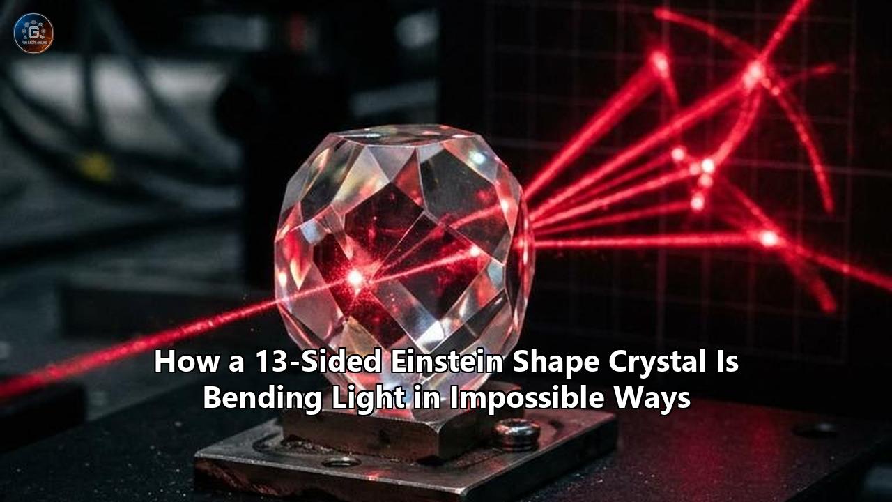
Physicists at the University of Tokyo and NTT Nanophotonics Center in Japan have constructed a nanostructured optical material based on a non-repeating mathematical pattern, demonstrating that it manipulates light in ways no conventional crystal can match. In a study published in Nature Communications, experimental physicist Yuto Moritake and senior author Masaya Notomi etched an array of nanoscale holes arranged in the geometry of the newly discovered 13-sided einstein shape onto a planar chip. When hit with a focused laser, the material produced a swirling, pinwheel-like optical diffraction pattern that reacts differently depending on whether the incident light spins clockwise or counterclockwise.
The achievement bridges a long-standing divide between theoretical geometry and optical physics. The underlying pattern—nicknamed "the hat"—was discovered by an amateur mathematician cutting cardstock at his kitchen table in 2022, solving a half-century-old mathematical quest known as the "einstein problem". By translating this single, non-repeating shape into physical photonic architecture, researchers have unlocked a phenomenon called two-dimensional chiral diffraction. The discovery offers optical engineers an entirely new method for controlling the polarization and propagation of light without relying on bulky three-dimensional structures.
                 HAT TILE GEOMETRY (13 SIDES)

                        /\
                       /  \
                  ____/    \____
                 |              |
                 |___        ___|
                     \      /
                     /      \
                ____/        \____
               |                  |
               |__________________|

  Key Physical Trait: Non-repeating space filling + Broken mirror symmetry
The Photonic Bottleneck: Why Conventional Crystals Hit a Wall
For decades, optical physics and telecommunications have relied on photonic crystals—materials patterned with repeating arrays of microscopic structures that act as traffic directors for light. By forcing light waves to interact with a strictly periodic lattice, engineers can trap specific wavelengths, bend light around tight corners, or filter optical signals.
However, strict periodic order imposes severe physical constraints:
- Directional Anisotropy: Light behaves differently depending on the angle at which it traverses a regular square or hexagonal grid, creating dead zones and unwanted optical reflections.
- Backscattering Sensitivity: Tiny manufacturing defects in a repeating grid disrupt the uniform periodic potential, causing light waves to scatter backward and degrade signal integrity.
- Dimensional Dependence for Chirality: Traditional flat (2D) photonic crystals possess mirror symmetry, rendering them incapable of distinguishing between left-handed and right-handed light polarization. Controlling light’s rotational state normally requires complex 3D helical structures that are difficult to manufacture on a semiconductor chip.
To bypass the limits of regular grids, researchers turned to quasicrystals—materials like Penrose tilings that display long-range structural order without local periodicity. Quasicrystals offer higher rotational symmetry and more uniform light scattering, but early implementations carried their own limitations.
Penrose tilings and similar quasicrystalline lattices require at least two distinct tile shapes (such as the "kite" and "dart") to cover a surface without repeating. This multi-tile requirement increases structural complexity during nanoscale lithography. Furthermore, conventional 2D quasicrystals possess intrinsic mirror symmetry. Because their spatial patterns look identical when flipped, they interact symmetrically with left- and right-handed light.
┌─────────────────────────┬───────────────────────────┬────────────────────────────┐
│ Lattice Architecture    │ Structural Unit           │ Optical Behavior           │
├─────────────────────────┼───────────────────────────┼────────────────────────────┤
│ Periodic Crystal        │ Single repeating tile     │ Anisotropic, non-chiral    │
│ Standard Quasicrystal   │ Two or more tiles         │ Isotropic, non-chiral      │
│ Einstein Monotile       │ Single 13-sided tile      │ Isotropic, strongly chiral │
└─────────────────────────┴───────────────────────────┴────────────────────────────┘
This structural limitation left optical engineers facing a choice: accept the spatial anisotropy and defect sensitivity of periodic grids, build difficult multi-tile quasicrystals, or attempt tedious 3D nanofabrication to achieve polarization control. The physical realization of an aperiodic monotile offers a way past this compromise.
The Math Behind the Metamaterial: Defining the Einstein Monotile
To understand why this nanostructured chip behaves so strangely, it helps to examine the geometry carved into its surface. In mathematics, the "einstein problem" asks whether a single shape can tile an infinite two-dimensional plane without gaps or overlaps, such that the resulting pattern never repeats. The name is a play on the German phrase ein Stein, meaning "one stone," and bears no direct relation to Albert Einstein.
In March 2023, David Smith, working alongside mathematicians Joseph Samuel Myers, Craig S. Kaplan, and Chaim Goodman-Strauss, published the proof for the first true aperiodic monotile: an irregular polykite composed of eight connected kites. Formally classified as a tridecagon, this 13-sided einstein shape fills flat space endlessly, but its global configuration never enters a periodic loop.
        13-SIDED MONOTILE ("HAT") VERTEX CONFIGURATION

                     (v3)-------(v4)
                     /             \
                   (v2)             (v5)
                   /                   \
                 (v1)                  (v6)
                   |                    |
                 (v13)                 (v7)
                   \                   /
                   (v12)             (v8)
                     \             /
                     (v11)-------(v10)---(v9)
The 13-sided hat tile possesses three key geometric properties that dictate its physical behavior when etched into matter:
- Strict Spatial Aperiodicity: The tile forces long-range order across infinite distances without allowing any finite patch to repeat periodically.
- Single-Tile Simplicity: Unlike Penrose tilings, which demand multiple building blocks, this structure builds an entire aperiodic continuum out of one single shape.
- Planar Chirality: The shape lacks a line of reflective mirror symmetry. To fill two-dimensional space completely, a small fraction (roughly 1 in 7) of the tiles must be flipped over into their mirrored counterpart.
When Yuto Moritake read about Smith’s discovery, he recognized an opportunity. "What is especially fascinating about the hat tile is that, although the resulting pattern appears irregular at first glance, it is actually constructed from the honeycomb lattice," Moritake noted. "We wanted to see whether this unique shape could also produce any unexpected physical phenomena."
Bending Light in Impossible Ways: The Discovery of Chiral Diffraction
The research team at the University of Tokyo and NTT translated the mathematical formula into hardware by using electron-beam lithography to carve thousands of microscopic 13-sided tile voids into a flat dielectric surface. Each void measured just hundreds of nanometers across, making the features smaller than the wavelength of visible light.
                      EXPERIMENTAL SETUP

    Circularly Polarized      Nanostructured Chip
        Laser Beam          (13-Sided Hole Pattern)      Chiral Diffraction
      ==============>      [░▒▓ █ ▓▒░ ░▒▓ █ ▓▒░]      =======> Swirling
      (Clockwise /          [▓▒░ ░▒▓ █ ▓▒░ ░▒]                 Pinwheel
    Counter-Clockwise)      [░ █ ▓▒░ ░▒▓ █ ▓▒]                 Pattern
When the team directed a laser beam perpendicular to the chip's surface, the light scattered off the aperiodic array, producing a far-field diffraction pattern. In a traditional photonic crystal with square geometry, light scatters into a simple four-point cross. In a hexagonal grid, it scatters into a six-point star.
The 13-sided hat tile produced something unexpected: a complex, continuous diffraction array shaped like a swirling pinwheel. Because the underlying tile pattern lacks mirror symmetry, the resulting optical diffraction map was asymmetrical.
The primary surprise occurred when researchers varied the polarization state of the incoming laser. Light can be circularly polarized, meaning its electric field vector rotates like a corkscrew—either clockwise (right-circularly polarized) or counterclockwise (left-circularly polarized) as it moves through space.
LEFT-CIRCULAR LIGHT               RIGHT-CIRCULAR LIGHT
   (Counter-Clockwise)                 (Clockwise)

         ↺                                ↻
       /   \                            /   \
      |  ↓  |                          |  ↓  |
       \___/                            \___/
         |                                |
         v                                v
┌─────────────────┐              ┌─────────────────┐
│  Hat Monotile   │              │  Hat Monotile   │
│ Photonic Lattice│              │ Photonic Lattice│
└─────────────────┘              └─────────────────┘
         |                                |
         v                                v
  Pinwheel Twists                  Pinwheel Twists
     Leftward                         Rightward
When left-handed circularly polarized light hit the chip, the pinwheel pattern scattered with a distinct directional intensity bias. When the team switched to right-handed light, the scattered pinwheel intensity inverted.
"We found that the diffraction patterns themselves become chiral because the structure lacks mirror symmetry," explained Masaya Notomi, senior author of the study. "This kind of optical response is fundamentally different from that observed in conventional quasicrystalline materials."
This optical handedness emerged from a completely flat, two-dimensional chip. In effect, the structural asymmetry of the 13-sided einstein shape was imprinted directly onto the physical momentum of light.
                 DIFFRACTION PATTERN COMPARISON

   Periodic Grid          Penrose Quasicrystal      Einstein Monotile

     .  *  .                   *   *                 \   /
      \ | /                   *  *  *                 \ /  (Swirling
    * - o - *                *   o   *             ---- o ---- Pinwheel)
      / | \                   *  *  *                 / \
     .  *  .                   *   *                 /   \

 (4-Fold Symmetry)        (10-Fold Symmetric)      (Asymmetric Chiral
  Symmetric Response       Non-Chiral Response      Polarization Shift)
Quantum Fluids and Mechanical Metamaterials: Broader Physical Properties
The Tokyo experiment is part of a broader wave of research testing how the 13-sided einstein shape behaves in physical systems beyond surface photonics.
                   PHYSICAL PLATFORMS FOR EINSTEIN MONOTILES

   ┌──────────────────────┐  ┌──────────────────────┐  ┌──────────────────────┐
   │ Nanophotonic Chips   │  │ Exciton-Polariton    │  │ Structural Lattices  │
   │                      │  │ Quantum Condensates  │  │                      │
   │ • Chiral diffraction │  │ • Macroscopic phase  │  │ • 246% strength boost│
   │ • Polarization       │  │   coherence          │  │ • Uniform stress     │
   │   filtering          │  │ • Ballistic flow     │  │   distribution       │
   └──────────────────────┘  └──────────────────────┘  └──────────────────────┘
Quantum Fluids of Light
At the Skoltech Photonics Center and the Tokyo Institute of Technology, a team led by Sergey Alyatkin explored how quantum fluids of light behave when trapped in an einstein-monotile geometry. The researchers optically sculpted an inorganic microcavity, generating exciton-polariton condensates—hybrid particles formed by the coupling of photons and electron-hole pairs—at the vertices of the 13-sided hat tiling.
When nonresonantly excited by structured laser pulses, the polaritons flowed ballistically out of each tile node, interacting with neighboring nodes across the non-repeating lattice. Despite the total absence of periodic symmetry, the quantum fluid synchronized into a unified, macroscopic coherent quantum state.
"We found a complex interference pattern in the plane of the microcavity sample as polaritons from different nodes ballistically propagate and interact," said Alyatkin. The study proved that long-range quantum coherence can be maintained within an enforced aperiodic monotile structure, opening new avenues for quantum simulation and topological light sources.
High-Strength Mechanical Metamaterials
The unique geometric properties of the monotile extend into solid mechanics. Materials scientists at Nanyang Technological University and collaborating institutions built 3D mechanical microlattices based on the 13-sided einstein shape.
Standard periodic microlattices tend to fail catastrophically along clear internal shear planes—the straight grid lines running through the material act as fault lines under heavy loads. The non-repeating nature of the einstein monotile prevents these shear planes from forming.
PERIODIC LATTICE FAILURE              EINSTEIN MONOTILE DISSIPATION

   |   |   |   |                         /   \   \   /
   |   |   |   |  <-- Shear fault       /  /___\   \  /  <-- Load redistributed
   |   |   |   |      line forms       /  /     \   \/       across non-linear
   |   |   |   |                         /       \           paths
In compression tests of interpenetrating phase composite (IPC) metamaterials made from 3D-printed titanium alloy (Ti-6Al-4V) filled with epoxy, the einstein-inspired microlattices demonstrated a 246.61% increase in compressive strength compared to standard periodic designs. By removing linear weakness pathways, the material distributes external stress evenly across its volume, absorbing up to 46.2 Joules per gram of mechanical energy.
Engineering Solutions: Overcoming the Implementation Gap
While the physical properties of the 13-sided einstein tile are compelling, translating a non-repeating geometric pattern into functional technology presents substantial engineering hurdles. Researchers and industry leaders are actively developing practical solutions to address these challenges:
┌──────────────────────────────┬──────────────────────────────┬──────────────────────────────┐
│ Technical Bottleneck         │ Engineering Consequence      │ Proposed Solution            │
├──────────────────────────────┼──────────────────────────────┼──────────────────────────────┤
│ Reflection vs In-Plane Flow  │ Light scatters off surface   │ Waveguide-coupled etched     │
│                              │ rather than through channels │ aperiodic channels           │
├──────────────────────────────┼──────────────────────────────┼──────────────────────────────┤
│ Flip-Tile Requirement        │ Mixed handedness dilutes     │ Transition to "Spectre"      │
│                              │ total chiral signal          │ chiral-pure monotiles        │
├──────────────────────────────┼──────────────────────────────┼──────────────────────────────┤
│ Large-Scale Design Complexity│ CAD software struggles with  │ Generative algorithmic       │
│                              │ infinite aperiodic layouts   │ tile-generation tools        │
└──────────────────────────────┴──────────────────────────────┴──────────────────────────────┘
Challenge 1: Transitioning from Scattering to Waveguiding
The initial breakthrough by Moritake and Notomi demonstrated chiral scattering—meaning light bouncing off the top of the chip was redirected in unusual ways. However, real-world optical chips and telecommunications hardware require light to travel inside the plane of the chip through embedded waveguides.
Solution: The Tokyo team is adapting the nanostructured array to function as a planar optical waveguide. By adjusting the depth and refractive index of the etched 13-sided holes, researchers aim to channel light through in-plane, non-repeating tracks. This approach could enable on-chip polarization splitters that route left- and right-handed light signals down different physical channels without requiring optical isolators or magnetic fields.Challenge 2: The "Flip-Tile" Contamination Problem
In the original 13-sided hat tiling, roughly 14% of the tiles must be inverted (flipped over into mirror images) to tile the plane without leaving gaps. This means that while the overall lattice lacks mirror symmetry, it contains small pockets of opposite handedness. These localized regions of opposite chirality partially offset the overall polarization effect, reducing optical efficiency.
ORIGINAL HAT TILE MIXTURE              PURE "SPECTRE" MONOTILE

  [Hat]  [Hat]  [FLIPPED]               [Spectre]  [Spectre]  [Spectre]
  [Hat]  [Hat]  [Hat]                   [Spectre]  [Spectre]  [Spectre]

  Contains ~14% inverted tiles           100% same-handedness tiles
Partially dilutes optical chirality Maximizes chiral optical responseChallenge 3: Algorithmic Simulation and Nanofabrication
Designing computer-aided design (CAD) files for standard optical chips is straightforward: engineers draw a single unit cell and program the software to loop it across a grid. Aperiodicity breaks this shortcut. Generating large-scale lithography masks for billions of non-repeating 13-sided tiles requires immense computational memory if designed manually.
Solution: Theoretical computer scientists have developed recursive substitution algorithms that generate aperiodic monotile coordinates programmatically. By defining hierarchical generation rules, optical engineers can generate defect-free nanoscale patterns across multi-centimeter silicon wafers in seconds.Broader Implications and Future Applications
The realization that a single aperiodic tile can fundamentally alter the behavior of light opens up several practical research avenues across photonics, communications, and material science:
                     FUTURE APPLICATIONS

        ┌───────────────────────────────────────────┐
        │        Optical Computing & Switches       │
        │ • Chiral routing without magnetic fields  │
        │ • Reduced optical cross-talk              │
        └─────────────────────┬─────────────────────┘
                              │
        ┌─────────────────────┴─────────────────────┐
        │      Compact Telecommunication Chips      │
        │ • Direct circular-polarization splitters │
        │ • Flat optical components (Metalenses)    │
        └─────────────────────┬─────────────────────┘
                              │
        ┌─────────────────────┴─────────────────────┐
        │      High-Energy Laser System Arrays      │
        │ • Defect-tolerant light amplification     │
        │ • Suppression of parasitic modes          │
        └───────────────────────────────────────────┘
Optical Computing and Signal Routing
Modern electronic processors generate excessive heat due to electrical resistance. Optical computing aims to replace electrical currents with light pulses, dramatically increasing processing speed while reducing power consumption. A primary obstacle in photonic integration is cross-talk: light traveling down one nano-channel often spills into adjacent channels.
By routing light through aperiodic monotile lattices, photonic integrated circuits can exploit chiral light states to enforce one-way optical paths. Because the non-repeating structure suppresses destructive backscattering and enforces strict polarization-dependent propagation, optical logic gates can operate closer together without signal interference.
On-Chip Polarization Sensors
Circularly polarized light plays a central role in biological sensing, pharmaceutical testing, and satellite telecommunications. Molecules such as glucose, proteins, and DNA are inherently chiral, absorbing left- and right-handed light differently.
Current polarimeters require multi-component optical trains with waveplates and rotating filters. A single sensor chip patterned with an array based on the 13-sided einstein shape could separate left- and right-handed light directly on a flat surface, shrinking a benchtop scientific instrument down to a microchip.
High-Power Lasers and Metasurfaces
In high-power semiconductor laser arrays, individual lasers tend to lock into unwanted lateral spatial modes that degrade beam quality. Photonic crystal surfaces patterned with aperiodic monotile geometries eliminate these regular mode paths. The resulting laser arrays can emit tightly focused, high-power beams with built-in polarization control, benefiting industrial laser machining and free-space optical communications.
What to Watch Next
The transition of the 13-sided einstein shape from a celebrated mathematical puzzle into a physical platform for manipulating light marks a turning point in metamaterial design. By demonstrating that a single non-repeating geometry can induce chiral diffraction on a flat chip, researchers have proved that long-range structural order without mirror symmetry creates unique optical capabilities.
In the coming years, several key milestones will determine how quickly this discovery moves from laboratory demonstration to commercial application:
- In-Plane Photonic Integration: Demonstrations of waveguided in-plane optical signals routed through 13-sided monotile channels rather than surface scattering arrays.
- Spectre Tile Realization: Fabrication of pure "Spectre" photonic metasurfaces that eliminate mirrored tiles entirely, maximizing chiral optical efficiency.
- Active Metamaterials: Merging the monotile geometry with phase-change materials (like GST or liquid crystals) to create dynamically reconfigurable, switchable chiral optical chips.
- 3D Volumetric Photonic Crystals: Extending the 2D planar monotile into three-dimensional aperiodic networks capable of omnidirectional light control.
As nanofabrication techniques continue to refine these complex geometries, the boundary between abstract pure mathematics and physical material science will continue to blur. The 13-sided tile that once existed only as a geometric concept is now guiding the future of optical technology.
Reference:
- https://www.livescience.com/physics-mathematics/crystal-made-from-13-sided-einstein-shape-bends-light-in-ways-nobody-imagined
- https://thedebrief.org/the-einstein-tile-that-broke-math-is-now-twisting-light-into-pinwheels/
- https://xenospectrum.com/en/einstein-tile-chiral-diffraction/
- https://www.thebrighterside.news/post/mathematical-tile-shaped-like-a-crooked-hat-solves-decades-old-einstein-problem/
- https://www.facebook.com/groups/tiled/posts/1029392833038769/
- https://blogs.mathworks.com/cleve/2025/03/27/the-hat-a-tridecagon-aperiordic-monotile/
- https://www.facebook.com/ScienceSprings/posts/from-the-university-of-tokyo-jp-a-new-twist-on-the-einstein-problem-reveals-unex/1656872425830975/
- https://www.maths.cam.ac.uk/features/tip-hat-celebrating-aperiodic-monotile-discovery
- https://arxiv.org/html/2307.11054v4
- https://www.theguardian.com/science/2023/apr/03/new-einstein-shape-aperiodic-monotile
- https://www.researchgate.net/publication/381955576_Unprecedented_Strength_Enhancement_Observed_in_Interpenetrating_Phase_Composites_of_Aperiodic_Lattice_Metamaterials
- https://www.researchgate.net/publication/404848607_Observation_of_an_aperiodic_polariton_monotile
- https://pmc.ncbi.nlm.nih.gov/articles/PMC12459408/
- https://www.tandfonline.com/doi/full/10.1080/17452759.2025.2505992
- https://www.researchgate.net/publication/408204817_Design_of_metamaterials_for_additive_manufacturing
- https://www.livescience.com/physics-mathematics/physicists-find-a-way-to-control-heat-in-a-way-once-thought-impossible
- https://metaconferences.org/META25/files/META2025_program.pdf