Modern Computing Hit a Wall at the Speed of Light. Physicists Just Found a Way to Pause It.
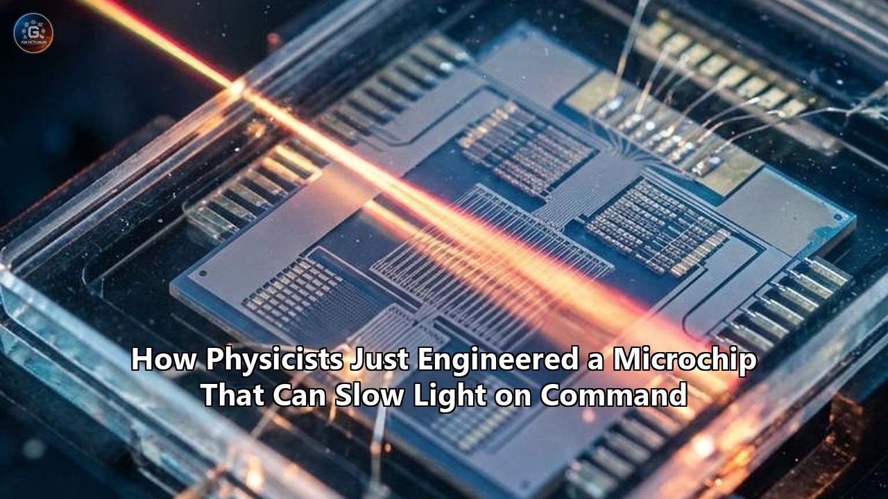
Researchers from Seoul National University and the University of Seoul announced the development of a programmable photonic integrated circuit capable of slowing down, delaying, and storing optical light pulses on command. Led by Professors Namkyoo Park and Sunkyu Yu at Seoul National University in collaboration with Professor Xianji Piao at the University of Seoul, the team demonstrated a device that dynamically alters the speed, temporal waveform, and frequency characteristics of light as it travels across a silicon chip.
This advance targets one of the most persistent bottlenecks in modern information technology: the inability to pause or buffer light without converting it back into electrical charges.
                 TRADITIONAL HYBRID ROUTING (HIGH POWER LOSS)
  [ Optical Input ] ---> [ Photo-Detector ] ---> [ SRAM Electronic Buffer ] ---> [ Laser Modulator ] ---> [ Optical Output ]
                            (O-E Conversion)         (High Energy & Latency)       (E-O Conversion)

                                PROGRAMMABLE SLOW LIGHT MICROCHIP (ZERO CONVERSION)
  [ Optical Input ] ---> [ Low-Loss Si3N4 Waveguide ] ---> [ Tunable CRIT Resonators ] ---> [ Optical Output ]
                                                            (On-Demand Optical Delay)
For decades, engineers faced a stark fundamental trade-off. Electrons are easy to stop, hold, and manipulate in transistors and capacitors, but moving them through copper wires generates immense heat, suffers from parasitic capacitance, and throttles data bandwidth. Photons move data at velocity $c$—nearly 300,000 kilometers per second—with virtually no resistance or heat generation.
Yet that same blistering speed makes photons notoriously slippery. Photons have zero rest mass; they cannot sit idly inside a memory cell waiting for a processor cycle.
When two optical data streams arrive at a photonic switch or an optical artificial intelligence accelerator at slightly different times, they cannot simply be stored in a physical register. To hold the data, hardware platforms must convert light signals into electrical signals, queue them in power-hungry electronic RAM, and re-transmit them as laser pulses. This conversion loop consumes up to 40 percent of the energy budget in high-performance computing interconnects.
By creating a programmable slow light microchip, the Korean research team has demonstrated an all-optical buffer. By dynamically tuning the group velocity of light directly inside integrated silicon nitride waveguides, their device introduces precise, reconfigurable optical delays without requiring electronic conversion. The realization provides a crucial missing building block for next-generation AI data centers, optical packet routers, and quantum networks.
The Optical Paradox: Why Light's Relentless Speed Creates a Data Bottleneck
To understand why controlling light's velocity on a chip is so difficult, one must examine how digital architectures process information. Modern microprocessors rely on strict temporal synchronization. Every arithmetic logic unit (ALU), cache line, and memory controller operates on system clocks that dictate precisely when data must arrive at a logic gate.
If signal A arrives five picoseconds ahead of signal B at an electronic AND gate, dynamic flip-flops hold signal A in place until signal B catches up.
In photonic computing, however, light does not pause naturally. When optical pulses propagate down standard silicon or silica waveguides, they move at the group velocity of the material:
$$v_g = \frac{c}{n_g}$$
where $c$ is the speed of light in a vacuum and $n_g$ is the group index of the waveguide medium. In silicon, with a refractive index of approximately 3.45, light travels at roughly 86,000 kilometers per second. While this speed allows data to cross a chip in picoseconds, it leaves zero margin for temporal misalignment.
                          TEMPORAL DESYNCHRONIZATION IN OPTICAL LOGIC

 Pulse A (Arrives t = 0 ps)   =====> [ Photonic Logic Gate ] =====> Flies past before processing
 Pulse B (Arrives t = 5 ps)   -------------------------> [ Photonic Logic Gate ] (Arrives too late!)
If two optical pulses inside a photonic matrix multiplier arrive out of phase, they cannot interact nonlinearly or perform logic operations together. The faster data travels, the harder it becomes to align, route, and queue.
This temporal mismatch creates severe operational friction across three primary domains:
- Artificial Intelligence Accelerators: Large language models and neural networks require trillions of multiply-accumulate (MAC) operations per second. Photonic tensor processing units (TPUs) use light interference to compute matrix products at the speed of light. However, accumulating intermediate results across deep network layers requires precise multi-nanosecond delays to prevent outputs from colliding.
- Data Center Optical Switching: Fiber-optic backbones transmit petabytes of data across server racks. When multiple data packets collide at a network switch node targeting the same output port, one packet must be queued. Because optical RAM has lacked practical realization, data centers rely on Optical-Electrical-Optical (O-E-O) transceivers. These components convert light into electrical currents, store the bits in standard DRAM, and convert them back to light via lasers. This cycle introduces severe thermal dissipation and millisecond-scale latency penalties.
- Quantum Information Networks: Photonic quantum computing relies on single-photon entanglement. Quantum repeaters and logic gates require single photons generated from probabilistic sources to arrive at beam splitters simultaneously. Without optical delay lines, quantum states cannot be held, causing quantum gate operations to fail.
Signal Smearing and Energy Bleed: Where Conventional Delay Lines Failed
Physicists and engineers have attempted to slow or store light on physical platforms for decades, but early techniques ran into prohibitive physical boundaries.
+--------------------------+------------------------------------+---------------------------------------+
| Approach                 | Operational Mechanism              | Primary Failure Mode                  |
+--------------------------+------------------------------------+---------------------------------------+
| Fiber Delay Coils        | Kilometer-long spools of glass     | Massive physical footprint; rigid,    |
|                          | fiber-optic cable                  | unprogrammable static delays          |
+--------------------------+------------------------------------+---------------------------------------+
| Atomic EIT               | Electromagnetically Induced        | Requires cryogenic systems, ultra-    |
| (Trapped Gas)            | Transparency in rubidium vapors    | high vacuum, and complex bench lasers |
+--------------------------+------------------------------------+---------------------------------------+
| Photonic Crystal         | Etched 2D periodic dielectric      | Catastrophic optical power loss via   |
| Waveguides               | nanostructures                     | sidewall scattering; unchangeable     |
+--------------------------+------------------------------------+---------------------------------------+
| Uncoupled Microrings     | Recirculating optical cavities     | Narrow optical bandwidth; severe      |
|                          |                                    | Group Velocity Dispersion (pulse distortion)|
+--------------------------+------------------------------------+---------------------------------------+
The Bulky Glass Spool Method
The most elementary optical delay line is physical length. To delay a light pulse by 10 nanoseconds, an engineer can pass it through approximately two meters of optical fiber. While effective in benchtop physics laboratories, spooling meters of glass fiber inside a server chassis is entirely unscalable. It offers zero dynamic adjustability; once the fiber is cut, the delay is permanently fixed.
Cryogenic Atomic Vapors
In 1999, a team led by Danish physicist Lene Hau at Harvard University made history by slowing light to 17 meters per second—and eventually stopping it completely—using an ultracold atomic cloud of sodium atoms cooled to near absolute zero. The team utilized Electromagnetically Induced Transparency (EIT), a quantum interference effect where a control laser renders an opaque atomic medium transparent to a probe laser within a narrow frequency band.
While a triumph for fundamental physics, EIT in atomic gases required vacuum chambers, magneto-optical traps, and complex laser systems. It could not be integrated into planar silicon fabrication lines or operated inside hot datacenter environments.
The Dispersion and Scattering Trap in Photonic Crystals
Seeking solid-state alternatives, researchers turned to nanostructured materials. In the mid-2000s, attempts were made using two-dimensional photonic crystal waveguides. By etching periodic arrays of nanoscale holes into silicon, engineers created artificial bandgaps that flattened the dispersion curve of light, forcing its group velocity down by factors of 100 to 1,000.
However, photonic crystal slow-light devices hit two engineering walls:
- Catastrophic Propagation Loss: As light slows down, its interaction time with the material increases, and its local electric field density surges. Any nanoscopic roughness on the etched sidewalls scatters the optical energy out of the waveguide. The light was indeed slowed, but 99 percent of the optical signal was lost to radiation before reaching the end of the chip.
- Group Velocity Dispersion (GVD): Slowing light through steep structural resonances causes different spectral components (frequencies) of a single light pulse to travel at drastically different speeds. A crisp digital pulse representing a "1" bit becomes smeared out over time as it propagates. This temporal broadening causes adjacent bits to overlap—a phenomenon known as Inter-Symbol Interference (ISI)—corrupting the data stream.
                           THE GROUP VELOCITY DISPERSION (GVD) PROBLEM

   Sharp Input Pulse (Bit '1')                      Dispersed Output Pulse (Bit Overlap)
       |                                                 _---_
      / \                                              _-     -_
     /   \                                            /         \
   _/_____\___                                      _/___________\___
t0 t1 t2 t0 t1 t2- Static Rigidity: Early silicon slow-light channels were static. Once etched into silicon, their optical properties were locked. If a system required a 5-picosecond delay instead of a 10-picosecond delay due to workload shifts, the chip was useless.
Engineers needed a solid-state platform that could achieve substantial slow-light factors while offering wide bandwidth, ultra-low optical loss, and real-time electronic programmability.
Coupled-Resonator Transparency: The Physics Behind the Programmable Buffer
The breakthrough engineered by the joint team from Seoul National University and the University of Seoul resolves these historical trade-offs through an integrated architecture based on Coupled-Resonator-Induced Transparency (CRIT).
             PROGRAMMABLE CRIT SCHEMATIC (SILICON NITRIDE PLATFORM)

        Bus Waveguide (In) ----------------------------------> Bus Waveguide (Out)
                               |                    |
                           Coupling             Coupling
                               |                    |
                           +-------+            +-------+
                           | Ring  | <========> | Ring  |
                           |  R1   | Inter-ring |  R2   |
                           +-------+ Coupling   +-------+
                               |                    |
                           [ Thermal ]          [ Thermal ]
                           [ Heater  ]          [ Heater  ]
Rather than forcing light through etched photonic crystal holes, the team built their slow light microchip out of custom-configured, low-loss silicon nitride ($Si_3N_4$) microring resonators evanescently coupled to a central bus waveguide.
Translating Atomic Physics to Integrated Photonics
CRIT is the classical, integrated-photonic analog of Electromagnetically Induced Transparency. Instead of using quantum mechanical interference between atomic energy levels, CRIT uses optical wave interference between multiple coupled optical cavities.
When a light wave propagates down the primary bus waveguide, it partial-couples into a primary microring resonator ($R_1$). If a secondary microring ($R_2$) is positioned adjacent to $R_1$, the light recirculates between the two resonant modes. By carefully tuning the coupling strengths ($\kappa_1, \kappa_2$) and the perimeter lengths of the microrings, the optical fields returning to the main bus waveguide undergo destructive phase interference.
This destructive interference carves out an extremely narrow, highly transparent transmission window directly inside a broader reflection or absorption band.
                                 CRIT OPTICAL SPECTRUM
   Transmission (T)
     1.0 |              /\  <-- Ultra-Narrow CRIT Transmission Window
         |             /  \     (Extreme steepness = Massive reduction in vg)
     0.5 |    \       /    \       /
         |     \_____/      \_____/
     0.0 +----------------------------------> Optical Frequency ($\omega$)
Inside this narrow spectral window, the phase response ($\phi$) of the transmitted light varies precipitously with frequency ($\omega$). Because group delay ($\tau_g$) is mathematically defined as the derivative of the phase shift with respect to frequency:
$$\tau_g = \frac{d\phi}{d\omega}$$
a steep variation in phase creates a massive, localized spike in optical group delay. The group velocity ($v_g = L / \tau_g$) plummets. Light passing through the system slows dramatically, effectively storing the photon energy within the localized electromagnetic fields of the coupled cavities before releasing it downstream.
Dynamic Reconfigurability via Thermo-Optic Phase Tuning
The central innovation of the SNU/University of Seoul design lies in its dynamic programmability. Previous CRIT implementations suffered from fixed optical responses. The Korean team integrated micro-scale metallic thermo-optic heaters directly above the silicon nitride microrings.
Silicon nitride possesses a stable thermo-optic coefficient ($dn/dT \approx 2.5 \times 10^{-5} \text{ K}^{-1}$). By applying local electric currents to the micro-heaters, the control system alters the local refractive index ($n$) of individual rings. This shifts their optical path lengths and changes the relative phase detuning between resonators in real time.
                     PROGRAMMABLE CONTROL FEEDBACK LOOP

 [ Integrated Photodetectors ] ---> [ FPGA/Control Logic ] ---> [ Micro-Heater Array ]
              ^                                                         |
              |                                                         v
              +------------------ [ Si3N4 CRIT Chip ] <-----------------+
As a result, operators can adjust three critical signal parameters on the fly:
- Variable Temporal Delay: The group delay can be swept continuously from zero picoseconds up to several nanoseconds simply by adjusting micro-heater voltage.
- Pulse Envelope Shaping: The device can compress, stretch, or reshape the temporal profile of passing optical pulses to match downstream logic gate requirements.
- Frequency Chirp Modulation: The chip can alter the spectral chirp of the pulse, compensating for external fiber dispersion elsewhere in the computing fabric.
"What we have demonstrated is a platform where light is no longer a passive passenger moving at fixed physical limits, but a manageable signal that can be held, formatted, and synchronized on demand inside standard photonic integrated circuits," noted the research team.
Parallel Advances: How Other Teams Are Slowing Light
The SNU design belongs to a broader wave of photonics innovations that emerged across 2024–2026, with laboratories globally exploring distinct material platforms to slow light down.
+------------------------------------+---------------------------------------+----------------------------------+
| Research Group / Institution       | Material Platform & Technique         | Key Performance Metric           |
+------------------------------------+---------------------------------------+----------------------------------+
| Seoul National University /        | Silicon Nitride ($Si_3N_4$) coupled   | Programmable, reconfigurable     |
| Univ. of Seoul (2026)              | CRIT micro-resonators                 | temporal delays & pulse shaping  |
+------------------------------------+---------------------------------------+----------------------------------+
| Univ. of Illinois Urbana-Champaign | Erbium-doped Lithium Niobate          | 1,000x slow-light factor via     |
| (Late 2025)                        | ($Er:LiNbO_3$) Spectral Hole Burning | reconfigurable spectral memory   |
+------------------------------------+---------------------------------------+----------------------------------+
| Chinese Academy of Sciences /      | Nanophotonic Crystal Waveguides       | >10,000x slowdown; 80% loss      |
| SIAT (2024)                        | with engineered band-edges            | reduction vs traditional designs |
+------------------------------------+---------------------------------------+----------------------------------+
Spectral Hole Burning in Lithium Niobate (UIUC)
In late 2025, physicists from The Grainger College of Engineering at the University of Illinois Urbana-Champaign, led by Professor Elizabeth Goldschmidt, demonstrated on-chip slow light using spectral hole burning in erbium-doped lithium niobate ($Er:LiNbO_3$).
By using an external pump laser to optically bleach a narrow absorption line within the rare-earth erbium ion ensemble, Goldschmidt’s team created a high-dispersion transparent window directly inside the lithium niobate waveguide. The technique achieved a slow-light factor near 1,000.
Because lithium niobate features a strong Pockels electro-optic effect, applying an electric field allows the optical properties of the window to be reconfigured continuously. The UIUC team demonstrated that spectral hole burning could provide both classical signal delay and quantum state storage for quantum computing protocols.
High-Efficiency Photonic Crystals (CAS)
Simultaneously, a research team led by Dr. Li Guangyuan at the Shenzhen Institute of Advanced Technology (SIAT), Chinese Academy of Sciences, re-engineered photonic crystal waveguides to overcome historical attenuation limits. By optimizing the geometry of periodic surface structures, SIAT slowed light down by more than 10,000 times while reducing energy dissipation losses by 80 percent compared to traditional designs.
"When light is slowed down, the energy density of the light increases dramatically," Dr. Li explained. "This means that within the same microscopic footprint, the effective interaction distance between light and matter is multiplied by thousands of times, dramatically enhancing device efficiency".
Erasing Distortion: How Engineers Solved the Dispersion and Loss Trap
Slowing light down on a silicon chip is only half the battle. Making that slowed light usable for high-speed computation requires overcoming two fundamental physical degradation modes: Group Velocity Dispersion (GVD) and Thermal Crosstalk.
Eliminating Pulse Smearing via Cascaded Resonance Tuning
When an optical pulse containing gigahertz or terahertz bandwidth enters a slow-light medium, its higher-frequency edge and lower-frequency edge experience different group velocities due to steep dispersion slopes. Left uncorrected, a sharp 10-picosecond pulse broadens into a weak, 100-picosecond blob, ruining high-bandwidth data transmission.
To solve this, the Seoul team designed a multi-stage, cascaded CRIT topology. By placing multiple ring pairs in series, each tuned to slightly offset resonant frequencies, the overall transfer function of the chip synthesizes a flat-top group delay spectrum.
                             FLAT-TOP GROUP DELAY PROFILE

      Group Delay ($\tau_g$)
         ^
         |         +-----------------+  <-- Flat-top delay region
         |        /                   \     (Zero GVD across pulse bandwidth)
         |       /                     \
         |      /                       \
         +-----------------------------------> Optical Frequency ($\omega$)
Inside this synthesized flat-top region, $\frac{d^2\phi}{d\omega^2} = 0$. This condition means that all frequency components within the signal’s bandwidth experience the exact same time delay. The pulse emerges from the slow light microchip delayed in time, but clean and crisp in shape, preserving bit integrity for downstream processing.
Taming Loss with Ultra-Low-Loss Silicon Nitride ($Si_3N_4$)
Historical slow-light chips fabricated on traditional Silicon-on-Insulator (SOI) waveguides suffered high propagation losses ($1.5 \text{ to } 3.0 \text{ dB/cm}$) because silicon's high refractive index contrast amplifies scattering off etched sidewall roughness.
The team solved this by using stoichiometric Silicon Nitride ($Si_3N_4$) buried in Silicon Dioxide ($SiO_2$) cladding. $Si_3N_4$ possesses a lower refractive index contrast ($n \approx 2.0$), which dramatically reduces scattering loss to below $0.1 \text{ dB/cm}$. Furthermore, $Si_3N_4$ has a wide bandgap, eliminating two-photon absorption (TPA)—a phenomenon that plagues silicon waveguides at high optical power levels.
Thermal Isolation Trenches Against Thermal Crosstalk
Because the programmable tuning relies on thermo-optic micro-heaters, placing dozens of rings closely together creates a risk of thermal crosstalk. Heat radiating from ring $R_1$ can drift into ring $R_2$, destabilizing the interference condition.
                 THERMAL ISOLATION TRENCH CROSS-SECTION

       [ Air Trench ]   [ Micro-Heater ]   [ Air Trench ]
             |                 |                 |
             v                 v                 v
      +--------------+  +--------------+  +--------------+
      |  SiO2 Clad   |  | Si3N4 Ring   |  |  SiO2 Clad   |
      +--------------+  +--------------+  +--------------+
      |               Silicon Substrate                  |
      +--------------------------------------------------+
To prevent heat bleed, engineers etched deep air-gap isolation trenches into the silicon dioxide substrate surrounding each microring. These thermal barriers confine heat strictly to the target cavity, lowering thermal cross-talk by over 25 dB and cutting the power needed to tune the optical delay to milliwatts per ring.
From AI Data Centers to Quantum Networks: Practical Applications on the Factory Floor
The ability to slow, store, and manipulate optical signals on a single chip addresses severe hardware constraints across multiple high-tech industries.
+-----------------------------------+------------------------------------------------------------------+
| Application Sector                | Role of Programmable Slow Light Microchip                        |
+-----------------------------------+------------------------------------------------------------------+
| AI Clusters & Photonic TPU        | Synchronizes optical weight and activation matrices inside       |
| Accelerators                      | photonic matrix multipliers without SRAM conversion steps        |
+-----------------------------------+------------------------------------------------------------------+
| Hyperscale Data Center            | Acts as an all-optical packet queue to resolve port contention, |
| Optical Routers                   | replacing high-power O-E-O transceiver buffers                   |
+-----------------------------------+------------------------------------------------------------------+
| Co-Packaged Optics (CPO)          | Provides microsecond signal alignment between adjacent xPU dies  |
|                                   | connected via optical interconnect fabrics                       |
+-----------------------------------+------------------------------------------------------------------+
| Quantum Communication             | Delays single-photon qubits to align probabilistic emission       |
| & Networks                        | events for Hong-Ou-Mandel interference and quantum repeaters    |
+-----------------------------------+------------------------------------------------------------------+
1. Eliminating the "Memory Wall" in Photonic AI Accelerators
Modern artificial intelligence models are choked by memory bandwidth limits. Photonic computing startups have developed optical matrix-vector multipliers that execute neural network inference thousands of times faster than electronic GPUs using laser interference.
However, complex networks require multi-layer processing. Layer 1 computes an output, which must then serve as the input for Layer 2. If Layer 2 is busy processing another data tensor, the optical output of Layer 1 must wait.
Without an optical buffer, that output must be routed to a photodetector, converted to digital SRAM memory, held, and re-emitted by a laser modulator.
             PHOTONIC TPU WITH INTEGRATED SLOW LIGHT BUFFER

  [ Input Vector ] ---> [ Photonic Layer 1 ] ---> [ Slow Light Buffer ] ---> [ Photonic Layer 2 ]
                                                      (Holds Light)
                                                      (Zero O-E-O)
Integrating a programmable slow light microchip into the optical path allows the output signal to be slowed down and held directly inside the optical domain. The light stays in motion as a wave, preserving phase and amplitude while waiting for Layer 2 to free up. This cuts pipeline latency and eliminates thousands of O-E-O conversion chips from the server board.
2. All-Optical Packet Queueing in Data Center Switches
In hyperscale cloud data centers (run by companies like Microsoft, Google, and Amazon), optical switches route petabytes of data between server racks. A major cause of packet loss is "port contention"—when two independent servers send data packets to the same destination switch port simultaneously.
Currently, switches resolve contention by dumping one packet into electronic SRAM queues.
By embedding programmable photonic delay arrays directly onto switch fabric line cards, incoming optical packets can be diverted into an optical delay loop. The packet is delayed by a precise number of nanoseconds until the target output port clears, then released into the network without ever leaving the optical domain.
                           ALL-OPTICAL PACKET QUEUEING

  Packet A (Target Port 1) ----> [ Switch Core ] --------------------------> Port 1 (Clear)
                                       |
  Packet B (Target Port 1) ------------+---> [ Slow Light Buffer ] ---------> Port 1 (Delayed)
                                             (Waits until Packet A clears)
3. Co-Packaged Optics (CPO) and Die-to-Die Interconnects
As monolithic silicon chip sizes reach physical reticle limits, semiconductor manufacturers are moving to multi-chiplet architectures (chiplets tied together on interposers). Advanced platforms rely on Co-Packaged Optics (CPO), replacing high-power electrical traces with microscopic optical waveguides running between chiplets.
On-chip optical delay buffers allow CPO fabrics to dynamically align clock signals across adjacent processing dies. If clock drift occurs between die A and die B due to local thermal fluctuations, the host system can alter the control voltage on the slow-light buffer, adjusting signal timing in real time to maintain zero-error communication.
4. Quantum Photonic Synchronization
In photonic quantum computing, entangling two photons via a Hong-Ou-Mandel (HOM) beam splitter requires the photons to be completely indistinguishable in frequency, polarization, and arrival time down to the femtosecond level.
Because quantum light sources (like spontaneous parametric down-conversion crystals) generate single photons probabilistically, photon A might be emitted at $t = 0 \text{ ps}$ while photon B is emitted at $t = 12 \text{ ps}$. By routing photon A through a reconfigurable slow-light delay channel, its path can be precisely lengthened by 12 picoseconds. Both photons then hit the beam splitter together, enabling reliable quantum logic operations.
The Manufacturing Horizon: Scaling Photonic Buffers into Foundry Production
The transition of slow-light photonics from physics laboratories to mass commercial deployment hinges on standard manufacturing processes. The choice of materials by the Seoul research team was deliberate: Silicon Nitride ($Si_3N_4$) is completely compatible with standard CMOS semiconductor fabrication facilities.
                               COMMERCIAL FABRICATION ROADMAP

  [ 300mm CMOS Foundry ] ---> [ DUV Photolithography ] ---> [ Deep Si3N4 Etch & Planarization ]
                                                                       |
  [ Packaging & Testing ] <--- [ Heterogeneous Laser Integration ] <----+
Unlike platforms relying on exotic atomic gases or non-standard crystalline matrices, silicon nitride photonic integrated circuits can be printed using existing Deep Ultraviolet (DUV) immersion lithography tools on standard 200mm and 300mm silicon wafers. Commercial foundries such as TSMC, GlobalFoundries, AIM Photonics, and Tower Semiconductor already offer standard foundry Process Design Kits (PDKs) for silicon nitride photonics.
Key Technical Milestones to Watch
As the technology advances toward industrial commercialization, engineers are working through several critical integration phases:
- Heterogeneous Integration with On-Chip Laser Sources:
Current prototypes require external optical laser inputs. Commercial production will require bonding Indium Phosphide (InP) or Gallium Arsenide (GaAs) lasers directly onto the silicon nitride slow-light substrate to create self-contained optical timing units.
- Closed-Loop Thermal Feedback Systems:
Data center operating environments experience dynamic temperature fluctuations as workloads surge. To maintain ultra-precise delays, future iterations of the slow light microchip will incorporate integrated Germanium photodetectors and automated closed-loop feedback circuits that monitor optical outputs and automatically adjust micro-heater drive currents.
- Expansion into Thin-Film Lithium Niobate (TFLN) Hybrids:
While thermo-optic heaters offer millisecond-to-microsecond reconfigurability, next-generation applications require nanosecond-scale switching speeds. Researchers are now exploring hybrid $Si_3N_4$-TFLN architectures, where electro-optic tuning will allow the speed of light on the chip to be modulated at gigahertz frequencies.
                  HYBRID $Si_3N_4$-TFLN ARCHITECTURE (NEXT-GEN)

     Electro-Optic Drivers (GHz Speed) ---> [ Thin-Film Lithium Niobate Layer ]
                                            [ Silicon Nitride Waveguide Layer ]
                                            [ Silicon Substrate Base         ]
By engineering a chip that converts the unrelenting speed of light from an unpredictable obstacle into a controllable resource, physicists have cleared a major hurdle in integrated optics. The ability to hold, format, and pause optical signals on a silicon chip marks a major step toward computing architectures where light does not just transport data—it controls, buffers, and processes it entirely on its own terms.
References
- --- SciTechDaily (July 25, 2026). "Scientists Built a Programmable Chip That Can Slow Light on Command." (Seoul National University & University of Seoul research findings on programmable CRIT photonic integrated circuits).
- --- ScienceDaily / Seoul National University College of Engineering (July 21, 2026). "New Chip Can Slow Light on Command." (Detailed report on Professors Namkyoo Park, Sunkyu Yu, and Xianji Piao's programmable photonic circuit).
- --- Alliance Chemical Tech Briefings (July 23, 2026). "Analysis of Silicon Nitride Programmable Slow Light Integrated Circuits." (Technical details on $Si_3N_4$ waveguides, CRIT interference, and thermal isolation trenches).
- --- South China Morning Post / SIAT Chinese Academy of Sciences (January 20, 2024). "Chinese Scientists Design Photonic Chip Reducing Light Speed by 10,000 Times." (Dr. Li Guangyuan's low-loss nanophotonic crystal slow-light research).
- --- Wikipedia & Historical Physics Archives. "Slow Light Background, Group Velocity Dispersion, and Electromagnetically Induced Transparency." (Lene Hau's 1999 Harvard experiments and foundational physics formulas).
- --- InformationWeek / IBM Research (November 3, 2005). "IBM Researchers Use Silicon Waveguides To Slow Light." (Early silicon photonic crystal waveguide historical background).
- --- University of Illinois Urbana-Champaign Grainger College of Engineering / Nature Communications (November 26, 2025). "Demonstration of Slow-Light Effect on Photonic Chips via Spectral Hole Burning."* (Prof. Elizabeth Goldschmidt's research on erbium-doped lithium niobate platforms).
Reference:
- https://scitechdaily.com/scientists-built-a-programmable-chip-that-can-slow-light-on-command/
- https://www.sciencedaily.com/releases/2026/07/260718010149.htm
- https://alliancechemical.com/blogs/news/seoul-researchers-develop-programmable-photonic-chip-that-can-slow-light-on
- https://www.scmp.com/news/china/science/article/3249173/chinese-scientists-say-they-slowed-down-light-improve-microchips
- https://www.eurekalert.org/news-releases/1119185
- https://iquist.illinois.edu/news/79523
- https://en.wikipedia.org/wiki/Slow_light
- https://www.informationweek.com/it-leadership/ibm-researchers-use-silicon-waveguides-to-slow-light