
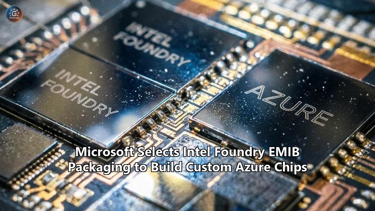
Microsoft and Intel announced a long-term agreement on November 18, 2026, establishing Microsoft as the first public customer for Intel Foundry EMIB (Embedded Multi-die Interconnect Bridge) advanced packaging to assemble custom Azure first-party processors. The deal pairs backend packaging services for Microsoft's proprietary accelerators and CPUs with a multi-year capacity guarantee for Intel Xeon server processors, including next-generation chips codenamed Diamond Rapids.
The disclosure landed on the same day Intel Chief Executive Officer Lip-Bu Tan announced at the TomorrowX summit in Austin that Intel had achieved 70% yields on its 18A (1.8-nanometer class) process and signed its first external customer for the performance-enhanced 18A-P node. While that foundry client’s identity was kept private, the public commitment from Microsoft centers squarely on the step after wafer manufacturing: advanced multi-die packaging.
+-----------------------------------------------------------------------------+
|                     MICROSOFT-INTEL AGREEMENT STRUCTURE                     |
+-----------------------------------------------------------------------------+
|                                                                             |
|  [ FRONT-END SILICON ]                 [ BACK-END INTEGRATION ]             |
|  * Disaggregated Sourcing              * Intel Foundry EMIB Assembly        |
|  * Heterogeneous Nodes (N3P/N2P/18A)   * EMIB-T Vertical Power Delivery     |
|                                        * Multi-Die Heterogeneous Bridge     |
|                                                                             |
|  [ SYSTEM DEPLOYMENT ]                 [ ENTERPRISE CO-DEVELOPMENT ]         |
|  * Maia AI Accelerators                * Xeon Diamond Rapids Deployments    |
|  * Cobalt Agentic ARM CPUs             * CXL Memory Tiering (M-series v4)   |
|                                        * Hardware QAT & TDX Confidential VM |
+-----------------------------------------------------------------------------+
Advanced packaging has emerged as the most acute physical bottleneck across high-performance computing and artificial intelligence hardware. By contracting Intel to package Azure silicon without tying those products to Intel’s front-end fabrication lines, Microsoft has executed a structural break from traditional single-foundry turnkey arrangements.
"Microsoft and Intel share a clear view of where AI infrastructure is headed—increasingly complex systems designed through the co-optimization of silicon, packaging, compute memory, and software," stated Naga Chandrasekaran, Executive Vice President, Chief Technology and Operations Officer, and General Manager of Intel Foundry.
Saurabh Dighe, Corporate Vice President of Azure System & Architecture at Microsoft, underscored that tailoring infrastructure around demanding hyperscale workloads requires "connecting silicon and systems engineering" by combining custom compute, memory tiers, security primitives, and packaging scale.
The immediate effect provides Microsoft an alternative to Taiwan Semiconductor Manufacturing Company’s (TSMC) heavily oversubscribed Chip-on-Wafer-on-Substrate (CoWoS) packaging lines. Over the medium and long term, the contract validates Intel Foundry’s open-ecosystem strategy, establishes a precedent for hyperscalers to disaggregate wafer fabrication from backend assembly, and alters the geopolitical risk profile of cloud infrastructure supply chains.
Deconstructing the Contract: Packaging as an Independent Service
The most technically consequential dimension of the Microsoft-Intel pact is its modularity. The joint release does not tie Microsoft's custom silicon to Intel's front-end fabrication lines, leaving Microsoft free to print compute tiles at external foundries while directing bare dies to Intel packaging facilities for final assembly.
+-----------------------------------------------------------------------------+
|             DISAGGREGATED FOUNDRY VS. TURNKEY MONOLITHIC MODEL              |
+-----------------------------------------------------------------------------+
|                                                                             |
|  TRADITIONAL TURNKEY (TSMC CoWoS):                                          |
|  [ Wafer Fab (TSMC) ] ---> [ Advanced Packaging (TSMC CoWoS) ] ---> Packaged |
|                                                                    Module   |
|                                                                             |
|  HYBRID DISAGGREGATED (Microsoft / Intel Foundry):                          |
|  [ Fab A (e.g. TSMC N3P/N2P) ] ---\                                         |
|                                    +--> [ Intel Foundry EMIB ] ---> Custom  |
|  [ Fab B (e.g. Memory / I/O) ] ---/                                 Azure   |
|                                                                    Module   |
+-----------------------------------------------------------------------------+
Hyperscalers designing internal silicon have historically relied on monolithic, turnkey contracts. When a cloud provider tapes out an accelerator with TSMC, the Taiwanese foundry typically fabricates the logic dies, sources the High Bandwidth Memory (HBM) base dies, manufactures the silicon interposer, and performs the CoWoS micro-bump bonding, thermal lid attachment, and final testing.
That turnkey approach creates a hard supply dependency. If backend packaging capacity lags behind wafer production—as occurred throughout 2023, 2024, and 2025 during the explosive ramp of enterprise AI—finished front-end wafers sit idle in nitrogen storage pods waiting for packaging allocation.
┌────────────────────────────────────────────────────────┐
│   Wafer Production (Compute, I/O, Transceivers)       │
│   Sourced across multiple foundry nodes (TSMC / Intel) │
└──────────────────────────┬─────────────────────────────┘
                           │
                           ▼
┌────────────────────────────────────────────────────────┐
│   Bare Die Dicing & Known Good Die (KGD) Sort          │
│   Parametric testing and micro-bump preparation        │
└──────────────────────────┬─────────────────────────────┘
                           │
                           ▼
┌────────────────────────────────────────────────────────┐
│   Intel Foundry EMIB Integration Facility              │
│   (Rio Rancho, New Mexico / Chandler, Arizona)         │
│   • Substrate Cavity Milling / Laser Ablation          │
│   • EMIB Bridge Embedding & Dielectric Lamination      │
│   • Sub-45µm Micro-Bump Die-to-Die Alignment          │
│   • EMIB-T Through-Silicon Via Vertical Power Connect  │
└──────────────────────────┬─────────────────────────────┘
                           │
                           ▼
┌────────────────────────────────────────────────────────┐
│   Final Package Assembly, Lid Attach & System Test     │
│   Multi-die Azure Custom Silicon Engine (Maia / Cobalt)│
└────────────────────────────────────────────────────────┘
The Microsoft deal marks the practical realization of Intel Foundry’s "systems foundry" premise: customers can purchase lithography, wafer manufacturing, or advanced packaging as distinct, decoupled service layers. Microsoft can print compute logic on TSMC's 3-nanometer (N3P) or 2-nanometer (N2P) process nodes, procure memory stacks directly from SK Hynix, Samsung, or Micron, and route those bare, tested dies to Intel packaging facilities in Oregon, New Mexico, or Arizona.
This uncoupling shifts procurement leverage away from monolithic foundries. Backend integration, once treated as a secondary phase of semiconductor manufacturing, has become the primary governor of cloud accelerator delivery timelines. Contracting for packaging as a discrete tier allows Microsoft to decouple its capital deployment from the packaging queues of any single vendor.
Technical Teardown: EMIB Engineering Against CoWoS
Advanced multi-die packaging is required because monolithic silicon dies have hit the physical reticle limit—the maximum area a deep-ultraviolet (DUV) or extreme-ultraviolet (EUV) photolithography scanner can expose in a single pass, fixed at approximately 858 square millimeters ($26\text{ mm} \times 33\text{ mm}$).
Building high-throughput AI accelerators requires total silicon surface areas ranging from 1,500 to over 3,000 square millimeters, spanning multiple logic tiles and 8 to 12 stacks of HBM. Connecting these disparate dies requires an interconnect density that standard organic printed circuit board (PCB) traces cannot deliver.
+-----------------------------------------------------------------------------+
|                      INTERCONNECT TOPOLOGY COMPARISON                       |
+-----------------------------------------------------------------------------+
|                                                                             |
|  TSMC CoWoS-S (Monolithic Interposer):                                      |
|  [ Compute Die A ]  [ Compute Die B ]  [ HBM Stack 1 ]  [ HBM Stack 2 ]     |
|  ======================================================================     |
|  [          FULL SILICON PASSIVE INTERPOSER (3x to 4x Reticle)         ]     |
|  ======================================================================     |
|  [                    ORGANIC PACKAGE SUBSTRATE                       ]     |
|                                                                             |
|  INTEL FOUNDRY EMIB (Embedded Silicon Bridges):                             |
|  [ Compute Die A ]  [ Compute Die B ]  [ HBM Stack 1 ]  [ HBM Stack 2 ]     |
|        ---                ---                ---                            |
|       | B |              | B |              | B |  <-- Silicon Bridges      |
|  =====+===+==============+===+==============+===+======================     |
|  [      ORGANIC BUILD-UP SUBSTRATE WITH EMBEDDED SILICON BRIDGES       ]     |
|                                                                             |
+-----------------------------------------------------------------------------+
The Physical Architecture of Intel Foundry EMIB
Intel Foundry EMIB solves the interconnect density problem by embedding tiny, ultra-high-density silicon bridges directly into carved cavities within the organic package substrate, rather than placing an expansive, full-sized silicon interposer beneath all components.
          [ ASIC Compute Tile ]                [ HBM Memory Stack ]
                    │                                    │
                    ▼                                    ▼
             ┌──────────────┐                     ┌──────────────┐
             │ Micro-Bumps  │                     │ Micro-Bumps  │
             │ (25-45µm)    │                     │ (25-45µm)    │
       ──────┴──────┬───────┴─────────────────────┴───────┬──────┴──────
                    │                                     │
                    │   ┌─────────────────────────────┐   │
                    └──►│   Embedded Silicon Bridge   │◄──┘
                        │   (Sub-2µm Line/Space routing)│
                        │   ┌─────┐         ┌─────┐   │
                        └───┤ TSV │─────────┤ TSV ├───┘
                            └──┬──┘         └──┬──┘
                               │               │  Vertical Power (EMIB-T)
       ────────────────────────┼───────────────┼────────────────────────
                               ▼               ▼
                 [ Organic Multi-Layer Substrate (ABF) ]
                               │
                               ▼
                    [ Ball Grid Array (BGA) ]
The bridge contains multiple redistribution layers (RDL) etched with sub-2-micrometer line and space geometries. These geometries match the ultra-fine contact pitch of high-performance silicon while bypassing the parasitic capacitance, latency, and signal degradation inherent in standard substrate routing.
- Substrate Cavity Fabrication: During manufacturing of the Ajinomoto Build-up Film (ABF) substrate, precise cavities are created using laser micro-machining or structural photolithography.
- Bridge Placement: The passive silicon bridge—fabricated on mature, highly yielding silicon wafers—is placed inside the cavity with sub-micron spatial tolerance.
- Dielectric Planarization: Organic build-up dielectric layers are applied over the bridge, and micro-vias are drilled to expose contact pads on both the silicon bridge and the surrounding substrate.
- Chip Assembly via Micro-Bumping: The logic compute tiles and HBM stacks are aligned over the substrate. The edge pins of adjacent dies mate directly to the fine-pitch pads of the embedded bridge (at bump pitches ranging from 45 down to 25 micrometers), while their central power and ground pins connect directly to standard package substrate pads.
+-----------------------------------------------------------------------------+
|                  PACKAGING ARCHITECTURAL METRIC COMPARISON                  |
+-----------------------------------------------------------------------------+
| METRIC                       | TSMC CoWoS-S          | INTEL FOUNDRY EMIB   |
+------------------------------+-----------------------+----------------------+
| Sub-Surface Interconnect     | Monolithic Interposer | Localized Silicon    |
|                              | (Etched Silicon)      | Bridge (Cavity)      |
+------------------------------+-----------------------+----------------------+
| Maximum Package Dimension    | ~3.3x–4x Reticle Limit| Modular Multi-Bridge |
|                              | (~2,800–3,400 mm²)    | (Over 4x Reticle)    |
+------------------------------+-----------------------+----------------------+
| Die-to-Die Interconnect Line | 0.8µm / 0.8µm to      | 1.0µm / 1.0µm to     |
| and Space (L/S)              | 0.4µm / 0.4µm         | 0.5µm / 0.5µm        |
+------------------------------+-----------------------+----------------------+
| Typical Bump Pitch           | 35–45 µm (Micro-bump) | 25–45 µm (Micro-bump)|
+------------------------------+-----------------------+----------------------+
| Substrate Warpage Profile    | High across large     | Moderate (Localized  |
|                              | full-area interposer  | silicon stiffness)   |
+------------------------------+-----------------------+----------------------+
| Thermal Expansion Mismatch   | Silicon interposer    | Silicon-to-organic   |
| (CTE: Si vs Organic)         | bonded to organic base| bridge boundary stress|
+------------------------------+-----------------------+----------------------+
| Power Delivery Path          | High-resistance TSVs  | Direct vertical feed |
|                              | through large interposer (EMIB-T TSV bypass) |
+------------------------------+-----------------------+----------------------+
| Relative Substrate Cost      | Substantially higher  | Lower (Standard ABF  |
|                              | (Large Si wafer area) | with localized Si)   |
+------------------------------+-----------------------+----------------------+
The Engineering Advantages of EMIB Over Monolithic Interposers
TSMC’s dominant CoWoS-S technology uses a large, monolithic passive silicon interposer positioned between the active logic/memory dies and the organic substrate. As processors expand beyond 2x, 3x, and 4x reticle limits to accommodate multi-tile accelerators, the silicon interposer itself becomes massive—often exceeding 2,500 to 3,000 square millimeters.
Producing monolithic silicon plates of this size introduces severe manufacturing liabilities:
- Interposer Defect Yield Loss: Any fatal particulate defect or crack across a 3,000 mm² interposer ruins the entire substrate, driving yield curves down exponentially as area grows.
- Thermal Expansion and Warpage: Silicon has a Coefficient of Thermal Expansion (CTE) of approximately $2.6 \times 10^{-6}/\text{K}$, while organic ABF substrates exhibit a CTE of roughly $12 \text{ to } 15 \times 10^{-6}/\text{K}$. Mating a massive, continuous sheet of thin silicon to an organic board creates intense thermo-mechanical shear stress during thermal cycling, causing corner lift, delamination, and solder fatigue.
- Power Delivery Inefficiencies: Monolithic silicon interposers require high-current power rails (supplying 1,000 or more amperes to advanced AI compute tiles) to travel vertically through hundreds of microscopic Through-Silicon Vias (TSVs) patterned across the interposer. The parasitic electrical resistance across these vertical columns causes voltage drop ($IR$ drop) and heat dissipation before power ever reaches the compute transistors.
Core power pins connect directly from the package substrate balls to the processor dies without passing through a high-resistance intermediate silicon layer. The diminutive size of the bridge (typically a few tens of square millimeters) eliminates the yield penalty of monolithic interposers: bridges yield at near 99% rates on mature lithography lines.
The Critical Role of EMIB-T in Microsoft's Azure Deployment
The specific architectural variant tapped by Microsoft includes EMIB-T. In early EMIB implementations, bridges were purely passive routing channels buried in the substrate, meaning components placed directly above the bridge could not receive electrical power from beneath. Die architects had to route all power around the perimeter of the bridge, limiting bridge placement along die margins.
       CORE LOGIC DIE LAYER
       ┌────────────────────────┐
       │   Transistor Fabric    │
       └───────────┬────────────┘
                   │
    ┌──────────────┴──────────────┐
    │  Micro-Bump Array (Signal)  │
    └──────────────┬──────────────┘
                   │
  ┌────────────────▼─────────────────────────────────────┐
  │  EMIB-T SILICON BRIDGE                               │
  │  ┌───────────────────────┐   ┌────────────────────┐  │
  │  │ Ultra-Fine Pitch RDL  │   │ Copper TSV Column  │  │
  │  │ (Die-to-Die Inter-    │   │ (Vertical Power    │  │
  │  │  connect Routing)     │   │  Delivery Feed)    │  │
  │  └───────────────────────┘   └─────────┬──────────┘  │
  └────────────────────────────────────────┼─────────────┘
                                           │
                        ┌──────────────────▼──────────────────┐
                        │ Direct Vertical High-Current Supply │
                        │ from Base Organic Substrate         │
                        └─────────────────────────────────────┘
EMIB-T introduces Through-Silicon Vias into the bridge silicon. This allows micro-bumps on the logic die above the bridge to draw power directly through the bridge from the base substrate.
For Microsoft’s custom chips, which operate at high current densities across tightly coupled matrix-multiplication arrays, EMIB-T enables vertical power delivery while maintaining high-density lateral routing interfaces for High Bandwidth Memory and adjacent compute dies. It eliminates localized power starving and removes routing constraints across high-power compute clusters.
Mapping Microsoft’s Custom Silicon Portfolio
Microsoft’s infrastructure architecture team has spent over a decade shifting core cloud workloads onto custom silicon, moving from off-the-shelf merchant processors to proprietary, workload-tailored ASICs.
+-----------------------------------------------------------------------------+
|                  MICROSOFT AZURE CUSTOM SILICON EVOLUTION                   |
+-----------------------------------------------------------------------------+
|                                                                             |
|  2023-2024 INITIAL DEPLOYMENTS:                                             |
|  • Azure Cobalt 100: 128-core ARM Neoverse N2 (TSMC N5, Monolithic)         |
|  • Azure Maia 100: 820mm² AI Accelerator (TSMC N5, Monolithic, 4x HBM2e)    |
|                                                                             |
|  2025-2026 MATURATION PHASE:                                                |
|  • Azure Cobalt 200: 132-core ARM Architecture (TSMC N3, Multi-Die)          |
|  • Azure Maia 200: High-density Inference Engine (TSMC N3P)                 |
|                                                                             |
|  2027+ NEXT-GENERATION (Intel Foundry EMIB Integration):                     |
|  • Azure Maia 300: Multi-chiplet compute topology, 8x HBM4 stacks,          |
|    ~950W TDP, modular packaging via EMIB-T                                  |
|  • Next-Gen Custom Azure Accelerators & Agentic Infrastructure Processors   |
|                                                                             |
+-----------------------------------------------------------------------------+
The Maia Accelerator Lineage
Microsoft unveiled the Azure Maia 100 AI accelerator in November 2023. Fabricated on TSMC's 5-nanometer node, Maia 100 was designed as a massive monolithic die approaching 820 square millimeters, paired with four stacks of HBM2e memory delivering 1.8 terabytes per second of bandwidth.
Maia 100 served as an infrastructure testbed for large language model inference and training runs on Microsoft Azure, specifically supporting workloads running within OpenAI’s GPT model families.
Monolithic designs face clear physical limits:
- Scaling Maia 100’s architecture to support modern reasoning models and agentic workflows required a marked increase in on-package SRAM, memory bandwidth, and compute arithmetic density.
- In late 2026, Microsoft rolled out Maia 200, an N3P silicon generation optimized for large-scale reasoning and deep inference loops.
- Looking to future deployments, Microsoft announced the architecture for Maia 300, shifting to a multi-chiplet layout utilizing advanced 2-nanometer class logic paired with eight stacks of next-generation HBM4 memory, pushing thermal design power past 950 watts.
+-----------------------------------------------------------------------------+
|                   MAIA 300 EMIB-T SYSTEM-LEVEL INTEGRATION                  |
+-----------------------------------------------------------------------------+
|                                                                             |
|   +-------+   +-------+   +-------+   +-------+   +-------+   +-------+     |
|   | HBM4  |   | HBM4  |   | HBM4  |   | HBM4  |   | HBM4  |   | HBM4  |     |
|   +---+---+   +---+---+   +---+---+   +---+---+   +---+---+   +---+---+     |
|       |           |           |           |           |           |         |
|     [EMIB]      [EMIB]      [EMIB]      [EMIB]      [EMIB]      [EMIB]      |
|       |           |           |           |           |           |         |
|   +---+-----------+-----------+---+   +---+-----------+-----------+---+     |
|   |     COMPUTE CHIPLET A         |   |     COMPUTE CHIPLET B         |     |
|   |     (Advanced Logic Node)     |---|     (Advanced Logic Node)     |     |
|   +-------------------------------+   +-------------------------------+     |
|                   |                               |                         |
|                 [EMIB]                          [EMIB]                      |
|                   |                               |                         |
|   +---------------+-------------------------------+---------------+         |
|   |           CENTRAL I/O & INTERCONNECT SWITCH TILE              |         |
|   +---------------------------------------------------------------+         |
|                                                                             |
+-----------------------------------------------------------------------------+
Maia 300 cannot be manufactured as a single monolithic block of silicon. The total physical surface area of the compute tiles, system I/O controller, and eight HBM4 base interfaces exceeds 2,500 square millimeters—far beyond the single-reticle boundary.
By contracting Intel Foundry to package these assemblies using EMIB-T, Microsoft can combine compute dies fabricated on external cutting-edge nodes with memory interface dies and high-density memory stacks onto a single package. The vertical power capability of EMIB-T routes the required 1,000 amperes directly to the compute tiles without incurring the thermal and resistive penalties seen with full-plate interposers.
The Cobalt CPU Roadmap
Complementing its accelerator portfolio, Microsoft introduced the Azure Cobalt 100 processor in late 2023: a 128-core Arm Neoverse N2 CPU designed to power general-purpose cloud computing, Microsoft Teams, SQL Server workloads, and containerized Azure microservices.
By late 2026, Microsoft scaled access to its Cobalt 200 platform, a 132-core custom ARM processor manufactured on TSMC’s 3nm family, rolling out the instances across 24 cloud regions.
Cobalt processors prioritize energy efficiency and memory bandwidth density per rack. As Microsoft architects successors to Cobalt 200, disaggregating the core CPU compute cluster from memory channels, PCIe Gen 6/Gen 7 PHYs, and security processors becomes essential.
Using Intel Foundry EMIB, Microsoft can partition high-core-count ARM compute tiles onto dense logic nodes while placing I/O transceivers and memory controllers on more cost-effective silicon nodes. EMIB connects these components with sub-nanosecond transit latency and multi-terabit interconnect bandwidth, achieving the latency characteristics of a monolithic CPU while preserving the yield and cost benefits of a modular chiplet architecture.
Resolving the Packaging Bottleneck
To understand why Microsoft secured backend packaging from Intel while retaining multi-foundry flexibility for wafer fabrication, the global packaging bottleneck must be analyzed across three operational vectors: lithography limits, substrate constraints, and supply chain concentration.
+-----------------------------------------------------------------------------+
|             ADVANCED AI ACCELERATOR VALUE AND BOTTLENECK CHAIN              |
+-----------------------------------------------------------------------------+
|                                                                             |
|  [ FRONT-END SILICON ]            [ MEMORY SUBSYSTEM ]                      |
|  TSMC / Intel Lithography         SK Hynix / Micron / Samsung               |
|  (EUV Scanner Capacity)           (DRAM Processing & TSV Stacking)          |
|             │                                    │                          |
|             └─────────────────┬──────────────────┘                          |
|                               ▼                                             |
|             [ PRIMARY STRUCTURAL BOTTLENECK ]                               |
|             Advanced Packaging Assembly (CoWoS / EMIB)                      |
|             • Specialized ABF Substrates                                    |
|             • Micro-Bumping & Ultra-Fine Die Alignment                      |
|             • Thermal Interface Material & Lid Processing                   |
|             • High-Yield Multi-Die Testing & Binning                        |
|                               │                                             |
|                               ▼                                             |
|             [ COMPLETED DATACENTER SYSTEM ]                                 |
|             Finished Cloud Accelerator Rack Assemblies                      |
|                                                                             |
+-----------------------------------------------------------------------------+
The Limits of Lithography and Reticle Constraints
The transition from general-purpose server workloads to foundation model training and inference accelerated the breakdown of traditional wafer scaling. Monolithic dies yield fewer functional units per wafer as die sizes grow.
$$\text{Defect Yield} \approx \left( 1 + \frac{D_0 \cdot A}{\alpha} \right)^{-\alpha}$$
Where:
- $D_0$ is the defect density per unit area.
- $A$ is the total physical area of the silicon die.
- $\alpha$ is the defect clustering parameter (typically between 1.0 and 2.0).
As die area $A$ approaches the photolithographic reticle boundary ($\sim 858\text{ mm}^2$), the yield of flawless monolithic silicon dies drops precipitously.
 Die Yield (%)
  100 |──────────────────────────┐
      |                          \
   80 |                           \
      |                            \
   60 |                             \
      |                              \  Monolithic Yield Cliff
   40 |                               \
      |                                \
   20 |                                 \
      |                                  \
    0 └───────────────────────────────────┴──────────
      0       200      400      600      800    1000
                        Die Area (mm²)
If an enterprise attempts to build a monolithic 800 mm² AI processor on a new 3nm process, a single defect destroys the entire chip.
Dividing that architecture into four 200 mm² chiplets shifts production from the steep drop-off curve back into the high-yield territory of 80% to 90%. However, this cost advantage is lost if the backend system used to bridge those four chiplets cannot be procured at scale, costs too much, or introduces assembly failures. Advanced packaging has ceased to be an ancillary assembly phase; it now dictates the underlying unit economics of high-performance computing.
The Substrate and Assembly Capacity Deficit
Between 2023 and 2026, the primary factor limiting the delivery of AI servers was not a lack of available cleanroom space for front-end photolithography. It was the shortfall in advanced packaging lines. TSMC spent billions expanding its CoWoS operations across Taiwan—opening Advanced Backend Fab 6 and expanding facilities in Taichung, Tainan, and Chiayi—yet demand consistently outstripped capacity.
Lead times for high-performance packaged accelerators stretched past 40 weeks, while market allocations favored massive merchant buyers like Nvidia, who held hundreds of billions of dollars in multi-year purchase and supply commitments.
Hyperscale operators pursuing in-house silicon programs—including Microsoft, Amazon Web Services, Alphabet, and Meta—found their hardware delivery schedules dependent on TSMC's packaging allocation boards. A hyperscaler could contract for sufficient wafer capacity on an N3 or N4 process node, only to wait months for an allocation window to bond those logic dies to HBM stacks on a CoWoS line.
Securing packaging through Intel Foundry EMIB diversifies Microsoft's supply chain. It allows Azure to source silicon from one ecosystem and package it within another, insulating its server deployment timelines from disruptions or capacity constraints at a single manufacturing point.
+-----------------------------------------------------------------------------+
|                 HYPERSCALE SUPPLY PIPELINE DIVERSIFICATION                  |
+-----------------------------------------------------------------------------+
|                                                                             |
|  SCENARIO A: Monolithic Turnkey Dependency                                  |
|  [ Compute Silicon ] ──► [ TSMC CoWoS Packaging ] ──► System Assembly      |
|  [ Memory Stacks   ] ──► (Cap Ex & Allocation Chokepoint)                  |
|                                                                             |
|  SCENARIO B: Microsoft Disaggregated Azure Supply                           |
|  [ TSMC N3P Wafers ] ──┐                                                    |
|  [ Intel 18A-P Wafers] ─┼──► [ Intel Foundry EMIB ] ──► Azure Datacenter    |
|  [ Micron/Hynix HBM] ──┘      (Independent Packaging Capacity Pipeline)     |
|                                                                             |
+-----------------------------------------------------------------------------+
Strategic Implications for Key Ecosystem Players
The agreement reshapes strategic assumptions across the semiconductor landscape, impacting five core constituencies.
+-----------------------------------------------------------------------------+
|                         ECOSYSTEM IMPACT MATRIX                             |
+-----------------------------------------------------------------------------+
|                                                                             |
|  [ INTEL FOUNDRY ]                     [ TSMC ]                             |
|  • Establishes modular packaging-      • Packaging near-monopoly breached   |
|    as-a-service model                  • Must compete on backend economics  |
|  • Bridges fab revenue gap ($411M ext) • Retains front-end wafer dominance  |
|  • Validates packaging capabilities    • Pressured to expand multi-foundry  |
|                                          interconnect support               |
|                                                                             |
|  [ MICROSOFT AZURE ]                   [ HYPERSCALE COMPETITORS ]           |
|  • Breaks single-source TSMC lock-in   • Blueprint for AWS, Google, Meta    |
|  • Lowers packaging lead times         • Multi-sourcing accelerates across  |
|  • Co-optimizes Xeon & custom chips      the custom ASIC ecosystem          |
|  • Mitigates Taiwan geographic risk    • UCIe interface adoption deepens    |
|                                                                             |
|                       [ MERCHANT SILICON (NVIDIA) ]                         |
|                       • Hyperscalers gain leverage on pricing               |
|                       • In-house ASICs gain predictability                 |
|                       • Multi-foundry packaging lowers barrier             |
|                         to custom silicon deployment                       |
+-----------------------------------------------------------------------------+
1. Intel Foundry: Validating the Systems Foundry Model
For Intel Foundry, this long-term agreement serves as an external operational milestone. Since establishing its standalone foundry operating structure, Intel has absorbed billions in operating losses while working to restore process parity through its aggressive five-nodes-in-four-years roadmap.
Intel CEO Lip-Bu Tan pointed out that external foundry revenue sat at just $411 million out of $6.7 billion in total foundry segment revenue in late 2026, with the remainder generated by internal product groups.
Winning a public commitment from Microsoft for EMIB packaging provides commercial validation from a tier-one hyperscaler. It demonstrates to other potential customers—such as Apple, Qualcomm, and Nvidia—that Intel Foundry can operate as a viable service provider without forcing them to abandon their existing wafer fabrication arrangements.
 Intel External Foundry Trajectory
 Revenue ($)
   ▲
   │                                     * Microsoft EMIB Scaling
   │                                  *
   │                               * High-Volume Packaging Ramp
   │                            *
   │                         * First 18A-P Customer Onboarded
   │                      *
   │                   *
   │  $411M Baseline ───
   │  (Internal Dominated)
   └────────────────────────────────────────────────────────► Time
     2025              2026             2027             2028
The commercial metrics validate the approach:
- Ecosystem Proof Point: Advanced packaging has a lower barrier to entry than front-end wafer fabrication. Potential customers who are reluctant to risk entire processor designs on Intel's 18A node can safely adopt Intel packaging for dies printed at other foundries.
- Fab Utilization Efficiencies: Advanced packaging lines at Intel's Fab 9 and Fab 11x in Rio Rancho, New Mexico, along with investments in Chandler, Arizona, run on distinct capital cycles. Packaging revenue scales rapidly and carries healthy margins once assembly lines hit high yields.
- Bridgehead for Future Wafer Contracts: Once a customer establishes physical design workflows, test scripts, and packaging integration lines with Intel Foundry, the friction of routing front-end wafer manufacturing to Intel’s future 14A or 18A-P nodes decreases significantly.
2. TSMC: The Cracking of a Packaging Near-Monopoly
TSMC has long used its CoWoS packaging technology as an effective competitive moat. By bundling front-end wafer lithography with proprietary backend integration, TSMC created high switching costs for its customers.
If a customer wanted CoWoS capacity, they had to manufacture their wafers on TSMC lines. Conversely, if a customer designed silicon for TSMC’s leading-edge nodes, relying on their internal packaging was the fastest, lowest-risk path to commercial deployment.
+-----------------------------------------------------------------------------+
|                      TSMC COMPETITIVE MOAT TRANSITION                       |
+-----------------------------------------------------------------------------+
|                                                                             |
|  HISTORIC DEFENSE (Tightly Bundled):                                        |
|  ┌─────────────────────────┐                                                |
|  │ TSMC Advanced Wafers    │──(Tightly Coupled)──► [ TSMC CoWoS Packaging ] │
|  └─────────────────────────┘                                                |
|                                                                             |
|  EMERGING MARKET REALITY (Disaggregated Services):                          |
|  ┌─────────────────────────┐                                                |
|  │ TSMC Advanced Wafers    │──(Transportable)───► [ Intel Foundry EMIB ]   |
|  └─────────────────────────┘                                                |
|  ┌─────────────────────────┐                                                |
|  │ External Logic Wafers   │────────────────────► [ TSMC CoWoS / CoWoS-L ]  |
|  └─────────────────────────┘                                                |
|                                                                             |
+-----------------------------------------------------------------------------+
Microsoft’s formal adoption of EMIB challenges that bundled model. It shows that high-volume hyperscalers are willing to split the manufacturing flow across multiple suppliers.
TSMC will maintain its lead in sheer advanced packaging volumes through 2027 and 2028, but its pricing flexibility faces new competitive pressure. Hyperscalers now have a viable second source capable of handling multi-die, fine-pitch integration at scale.
3. Rival Cloud Hyperscalers: Blueprint for Infrastructure Independence
Microsoft’s strategic shift provides a clear playbook for its cloud computing peers.
+-----------------------------------------------------------------------------+
|                      HYPERSCALER CUSTOM SILICON MATRIX                      |
+-----------------------------------------------------------------------------+
| OPERATOR    | CUSTOM SILICON FLEET        | TRADITIONAL PACKAGING | EMIB   |
|             |                             | ECOSYSTEM             | STATUS |
+-------------+-----------------------------+-----------------------+--------+
| Microsoft   | Maia 100/200/300,           | TSMC CoWoS-S / CoWoS-L| ACTIVE |
|             | Cobalt 100/200              |                       | CLIENT |
+-------------+-----------------------------+-----------------------+--------+
| Google      | Cloud TPU v5p, v6 Trillium, | TSMC CoWoS            | UNDER  |
|             | TPU v7, TPU v9 (MediaTek)   |                       | REVIEW |
+-------------+-----------------------------+-----------------------+--------+
| Amazon AWS  | Trainium 2/3, Inferentia 2, | TSMC CoWoS / OSATs    | EVAL-  |
|             | Graviton 4/5                | (Amkor, ASE)          | UATING |
+-------------+-----------------------------+-----------------------+--------+
| Meta        | MTIA v1, MTIA v2            | TSMC CoWoS            | WATCH- |
|             | (Inference & Training)      |                       | ING    |
+-------------+-----------------------------+-----------------------+--------+- Google Cloud: Supply-chain analyses point to Google’s TPU v9—designed in partnership with MediaTek—evaluating Intel Foundry’s EMIB-T packaging to support its high-density routing and power delivery requirements. Google has long prioritized supply chain resilience and was among the earliest adopters of custom ASIC infrastructure.
- Amazon Web Services (AWS): Through Annapurna Labs, AWS continues to scale its Trainium and Inferentia AI families, alongside its Graviton CPU line. Constrained CoWoS capacity has directly limited AWS’s ability to deploy Trainium 2 clusters at scale. Adopting an open, multi-foundry packaging posture relieves those deployment bottlenecks.
- Meta Platforms: Meta's internal MTIA (Meta Training and Inference Accelerator) efforts are critical to lowering the massive capital expenditures tied to its open-source AI infrastructure. As Meta scales MTIA designs across recommendation systems and generative models, relying on a single packaging provider presents a clear operational risk.
Azure Systems Architecture: Beyond Packaging
While advanced packaging garnered the primary headlines, the agreement establishes a deeply integrated systems architecture roadmap between Microsoft and Intel.
Modern cloud infrastructure is not composed solely of isolated AI accelerators; it requires a balanced topology of host server processors, memory hierarchies, high-speed fabrics, and virtualization hardware.
+-----------------------------------------------------------------------------+
|             INTEGRATED AZURE ENTERPRISE SYSTEMS ARCHITECTURE                |
+-----------------------------------------------------------------------------+
|                                                                             |
|  [ HOST CPU LAYER ]                                                         |
|  Next-Generation Intel Xeon Diamond Rapids (Xeon 7)                         |
|  • High IPC Performance Cores                                               |
|  • Native PCIe Gen 6 Integration & CXL 3.1 Host Controllers                 |
|                                                                             |
|  [ SYSTEM MEMORY CO-OPTIMIZATION ]                                          |
|  • CXL Flat Memory Mode (Azure M-series v4 VMs)                             |
|  • Up to 2.3x performance and dynamic memory capacity expansion             |
|                                                                             |
|  [ HARDWARE ACCELERATION ENGINE ]                                           |
|  • Intel QuickAssist Technology (QAT)                                       |
|  • Delivers up to 2.5x faster native SQL Server database backups            |
|                                                                             |
|  [ DATA SECURITY & TENANT ENCLAVES ]                                        |
|  • Intel Trust Domain Extensions (TDX)                                      |
|  • Real-time confidential live migration across hypervisor hosts            |
|                                                                             |
+-----------------------------------------------------------------------------+
Xeon Diamond Rapids and the CXL Memory Layer
The agreement confirms multi-year capacity allocations for Intel Xeon CPUs across Azure, highlighted by next-generation processors codenamed Diamond Rapids.
Diamond Rapids introduces updated performance cores built on Intel's advanced manufacturing nodes, bringing integrated Compute Express Link (CXL) controllers to market.
                      ┌────────────────────────────┐
                      │ Intel Xeon Diamond Rapids  │
                      │ (Host Enterprise CPU)      │
                      └─────────────┬──────────────┘
                                    │
               ┌────────────────────┴────────────────────┐
               │                                         │
        Native DDR5 Bus                           PCIe Gen 6 / CXL
               │                                         │
               ▼                                         ▼
   ┌───────────────────────┐                 ┌───────────────────────┐
   │ Low-Latency Local     │                 │ CXL Memory Controller │
   │ Memory Pool           │                 │ (Flat Memory Mode)    │
   └───────────────────────┘                 └───────────┬───────────┘
                                                         │
                                                         ▼
                                             ┌───────────────────────┐
                                             │ Pooled Dynamic Cloud  │
                                             │ Memory Expansion (2.3x│
                                             │ Performance Gain)     │
                                             └───────────────────────┘
A major challenge in hyperscale virtual machines is "memory stranding"—a condition where all CPU compute cores within a server blade are rented out to tenants, but gigabytes of installed physical DRAM sit idle and unallocated because they cannot be addressed dynamically across system buses.
Integrating Intel Xeon processors equipped with CXL into Azure M-series v4 virtual machines enables CXL Flat Memory Mode:
- CXL establishes a cache-coherent interconnect between the CPU host, accelerator tiles, and external pooled DRAM buffers.
- Azure M-series v4 VMs achieve up to 2.3x greater performance and substantially improved memory flexibility for data-heavy workloads like SAP HANA and in-memory transactional databases.
- Memory can be dynamically partitioned, expanded, and reassigned across virtual machines without requiring expensive hardware reboots or physical memory reconfiguration.
Silicon Security and Workload Acceleration: QAT and TDX
The systems partnership extends directly into dedicated workload offloading and confidential virtualization:
- Intel QuickAssist Technology (QAT): By deploying hardware-accelerated QAT directly inside Azure virtual machines, Microsoft achieved up to 2.5x faster backup performance for mission-critical enterprise SQL databases. QAT offloads intensive symmetric cryptography, public key exchange, and data compression cycles from the main CPU cores, freeing host compute cycles exclusively for customer application workloads.
- Intel Trust Domain Extensions (TDX) Confidential Computing: Enterprise customers operating in strictly regulated sectors—such as defense, healthcare, and global finance—increasingly demand confidential computing environments where data remains fully encrypted while in use, even from the hypervisor itself. Microsoft’s implementation of Intel TDX enables hardware-isolated virtual environments called Trust Domains (TDs). The new agreement expands this architecture to support confidential live migration, allowing Azure to move running, encrypted virtual machines between physical server blades without exposing CPU register states or system memory to host-level security vulnerabilities.
Short-Term Realities: The 12-to-24 Month Horizon
While the high-level strategy offers clear benefits, executing a disaggregated packaging agreement across separate companies introduces demanding operational challenges that both engineering teams must navigate over the next 12 to 24 months.
+-----------------------------------------------------------------------------+
|              12-TO-24 MONTH OPERATIONAL ROADMAP & CHALLENGES                |
+-----------------------------------------------------------------------------+
|                                                                             |
|  [ KNOWN GOOD DIE (KGD) SORTING ]                                           |
|  • Cross-company electrical test qualification                              |
|  • Resolving finger-pointing between external fab and packaging house       |
|                                                                             |
|  [ SUBSTRATE WARPAGE & THERMAL ENGINEERING ]                                |
|  • Managing CTE mismatches across hybrid packaging interfaces               |
|  • Dissipating >950W heat flux across heterogeneous multi-die surfaces      |
|                                                                             |
|  [ ASSEMBLY LINE BRING-UP ]                                                 |
|  • Ramping specialized bridge-placement tools at Fab 9 / Fab 11x            |
|  • Achieving sustained packaging yield rates above 95% at scale             |
|                                                                             |
+-----------------------------------------------------------------------------+
Known Good Die (KGD) Sort and Cross-Foundry Liability
The operational friction in a split manufacturing model lies in resolving yield liability across vendors. In a turnkey TSMC CoWoS flow, TSMC is responsible for both the wafer and the packaging. If an assembled accelerator fails functional testing due to a bridge fracture or micro-bump short, a single vendor absorbs the financial loss.
When Microsoft routes bare dies from an external foundry to an Intel packaging line, establishing root-cause failure requires rigorous parametric testing:
- Known Good Die Sorting: Microsoft must implement exhaustive wafer-level screening and built-in self-test (BIST) routines at the external fab before dies are diced and shipped. A single marginal transistor inside a compute tile must not pass through to backend assembly, where it would compromise an expensive package containing multiple HBM4 stacks.
- Standardized Interconnect Probing: Fine-pitch micro-bumps (sub-45 micrometer) cannot easily be contacted by physical probe cards without damaging the delicate copper-pillar structures. Advanced contactless or sacrificial-pad test methodologies must be deployed to verify I/O integrity before the dies are committed to the EMIB assembly process.
- Contractual Defect Accounting: Microsoft, Intel Foundry, and the front-end fabrication partners must maintain strict service level agreements that cleanly delineate whether an assembly failure was caused by a latent silicon defect, handling damage during transit, or a bonding failure within the EMIB bridge cavity.
Mechanical Warpage and Thermal Budgets Above 950 Watts
Next-generation accelerators like Maia 300 operate within extreme thermal envelopes, dissipating between 950 and 1,200 watts across an expansive multi-tile layout. Dissipating that level of heat flux creates substantial physical stress:
        HIGH-EFFICIENCY VAPOR CHAMBER / DIRECT-TO-CHIP LIQUID COLD PLATE
     ══════════════════════════════════════════════════════════════════════════
     ▓▓▓▓▓▓▓▓▓▓▓▓▓▓▓▓▓▓▓▓▓▓▓  Thermal Interface Material  ▓▓▓▓▓▓▓▓▓▓▓▓▓▓▓▓▓▓▓▓
     ┌──────────────────────┐                          ┌─────────────────────┐
     │ COMPUTE TILE A       │                          │ HBM4 MEMORY STACK   │
     │ Operating at ~100°C  │                          │ Max Temp: ~85°C     │
     └──────────┬───────────┘                          └──────────┬──────────┘
                │   CTE: ~2.6 ppm/K                               │
     ───────────┴─────────────────────────────────────────────────┴───────────
     [ ORGANIC BUILD-UP PACKAGE SUBSTRATE ]  CTE: ~14.0 ppm/K
     ▲▲▲▲▲▲▲▲▲▲▲▲▲▲▲▲▲▲▲▲▲▲▲▲▲▲▲▲▲▲▲▲▲▲▲▲▲▲▲▲▲▲▲▲▲▲▲▲▲▲▲▲▲▲▲▲▲▲▲▲▲▲▲▲▲▲▲▲▲▲▲▲▲
HIGH THERMAL EXPANSION SHEAR STRESS ZONE (Substrate Warpage Risk)- Thermal Gradients Across Adjacent Silicon: A compute tile running matrix multiplication can reach temperatures up to 100°C, while an adjacent HBM4 stack must remain below 85°C to prevent data corruption and refresh degradation. This sharp temperature gradient over just a few millimeters of space induces asymmetric thermal expansion across the package.
- Substrate Warpage Management: Because the bulk of the EMIB package uses an organic build-up substrate, its thermal expansion rate ($CTE \approx 14 \text{ ppm/K}$) is much higher than that of the localized silicon bridges ($CTE \approx 2.6 \text{ ppm/K}$). As the package cycles between idle states and maximum compute bursts, mechanical shear stress concentrates along the micro-bumps at the edge of the bridge. Intel Foundry must use advanced underfill materials and structural stiffening rings to prevent micro-bump fatigue, solder cracking, or substrate delamination over Azure's multi-year deployment lifecycles.
Long-Term Structural Shifts: The 3-to-5 Year Horizon
Looking beyond near-term deployment milestones, Microsoft’s integration of Intel Foundry EMIB sets into motion three long-term structural shifts that will reshape the broader computing industry through 2030.
+-----------------------------------------------------------------------------+
|             LONG-TERM STRUCTURAL SHIFTS IN GLOBAL COMPUTING                 |
+-----------------------------------------------------------------------------+
|                                                                             |
|  [ GEOPOLITICAL DIVERSIFICATION ]                                           |
|  • Onshoring backend advanced packaging within the United States            |
|  • Rebalancing the geographic risk concentrated across the Taiwan Strait    |
|                                                                             |
|  [ DIE-TO-DIE INTERCONNECT STANDARDIZATION ]                                |
|  • Deepened industry transition to Universal Chiplet Interconnect Express    |
|  • Multi-foundry modular mix-and-match chiplet marketplaces                 |
|                                                                             |
|  [ MONOLITHIC FOUNDRY DE-COUPLING ]                                         |
|  • Uncoupling front-end wafer fabrication from backend packaging services   |
|  • Hyperscalers command greater supply chain transparency and pricing power |
|                                                                             |
+-----------------------------------------------------------------------------+
1. Geopolitical Risk Rebalancing
The concentration of advanced packaging inside Taiwan has long represented a notable geographic risk point for global technology infrastructure. Even if an enterprise manufactures wafers inside the United States—utilizing TSMC’s Fab 21 in Phoenix, Arizona, or Intel’s facilities in Oregon and Ohio—most high-end packaged systems have historically had to return to East Asia for final backend assembly, HBM bonding, and test integration.
This arrangement undermined the primary goals of the U.S. CHIPS and Science Act: establishing complete, domestic supply chain security for mission-critical hardware.
By scaling high-volume EMIB-T packaging across Intel’s domestic manufacturing sites in New Mexico and Arizona, Microsoft establishes a viable path toward fully onshore advanced multi-die packaging.
 Traditional Silicon Logistics Route:
 [ US Fab (Wafer) ] ──► [ Air Freight to Asia ] ──► [ Packaging / Test ] ──► [ US Cloud Datacenter ]
 (Significant Transit Latency, Customs, and Geopolitical Concentration Risk)

 Microsoft-Intel Domestic Packaging Pipeline:
 [ Leading-Edge Fab ] ──► [ Intel Fab 9 / 11x New Mexico (EMIB) ] ──► [ US Cloud Datacenter ]
 (Reduced Transit Cycles, Secure Domestic Supply Chain Boundary)
This domestic packaging corridor provides Azure with a resilient hardware pipeline capable of supplying U.S. public sector workloads, defense intelligence networks, and enterprise cloud zones, largely protected from geopolitical trade restrictions or regional supply interruptions.
2. The Acceleration of Open Chiplet Architectures (UCIe)
The separation of packaging from wafer fabrication accelerates the semiconductor industry's transition toward the Universal Chiplet Interconnect Express (UCIe) standard.
               ┌─────────────────────────────────────────┐
               │         COMPUTE TILE (Any Node)         │
               │   ┌─────────────────────────────────┐   │
               │   │      UCIe Controller & Link     │   │
               └───┴────────────────┬────────────────┴───┘
                                    │
                                    ▼
                         ┌────────────────────┐
                         │   Die-to-Die PHY   │
                         └──────────┬─────────┘
                                    │
             Standardized D2D Bus   ▼ (Sub-45µm Pitch)
     ════════════════════════════════════════════════════════════════════
     [ INTEL FOUNDRY EMIB HIGH-DENSITY INTERCONNECT SILICON BRIDGE ]
     ════════════════════════════════════════════════════════════════════
                                    ▲
                         ┌──────────┴─────────┐
                         │   Die-to-Die PHY   │
                         └──────────┬─────────┘
                                    │
               ┌────────────────────┴────────────────┐
               │   │      UCIe Controller & Link     │   │
               │   └─────────────────────────────────┘   │
               │         I/O CONTROLLER / HBM DIE        │
               └─────────────────────────────────────────┘
Historically, connecting multiple dies inside a custom package required proprietary physical layers and closed protocol stacks developed in-house. A company was largely forced to use a single foundry’s proprietary interface to ensure adjacent dies could communicate reliably.
UCIe establishes an open, cross-industry standard defining the die-to-die physical layer, protocol multiplexing, and electrical interface:
- With major players like Microsoft, Intel, AMD, and Arm supporting the UCIe consortium, EMIB acts as a physical transport medium for standard UCIe-compliant chiplets.
- Over the next three to five years, this standardization enables a modular "chiplet marketplace." A hyperscaler can purchase specialized optical transceiver dies from one vendor, secure high-efficiency memory tiles from another, and bond them to proprietary logic chips using standard Intel Foundry EMIB assembly lines.
- Custom ASIC development will shift from an expensive, all-or-nothing engineering investment to an exercise in targeted system integration.
3. The Decoupling of the Monolithic Foundry Business Model
The agreement accelerates the unbundling of the traditional semiconductor foundry model. For nearly four decades, the foundry business operated on a bundled footing: contract chipmakers sold finished, processed wafers, offering packaging primarily to secure high-margin lithography orders.
As backend packaging costs climb toward 30% to 40% of total bill-of-materials costs for AI processors, advanced packaging is evolving into a standalone market.
+-----------------------------------------------------------------------------+
|                THE STRUCTURAL UNBUNDLING OF FOUNDRY SERVICES                |
+-----------------------------------------------------------------------------+
|                                                                             |
|  PAST (1995-2023): Bundled Monolithic Model                                 |
|  ┌───────────────────────────────────────────────────────────────────────┐  |
|  │                        TURNKEY CONTRACT CHIPMAKER                     │  |
|  │  [ Silicon Ingot ] ──► [ Lithography Fab ] ──► [ Packaging Assembly ] │  |
|  └───────────────────────────────────────────────────────────────────────┘  |
|                                                                             |
|  FUTURE (2027+): Modular Disaggregated Sourcing                             |
|  ┌───────────────────────────────────────────────────────────────────────┐  |
|  │ Layer 1: Advanced Lithography Services (TSMC / Intel Foundry / Samsung)│  |
|  ├───────────────────────────────────────────────────────────────────────┤  |
|  │ Layer 2: Specialized Packaging Platforms (Intel EMIB / TSMC CoWoS)    │  |
|  ├───────────────────────────────────────────────────────────────────────┤  |
|  │ Layer 3: Memory Subsystem Integration (SK Hynix / Micron / Samsung)   │  |
|  └───────────────────────────────────────────────────────────────────────┘  |
|                                                                             |
+-----------------------------------------------------------------------------+
Foundries will increasingly compete for distinct layers of the manufacturing stack. Intel Foundry has demonstrated that an organization can win an advanced packaging contract with a premier cloud hyperscaler even when its leading-edge wafer lithography business is running separate product lines.
This modularity forces every market participant—from TSMC to outsourced semiconductor assembly and test (OSAT) providers like Amkor and ASE—to adjust their pricing models and open their packaging lines to wafers arriving from competing foundries.
Critical Milestones and Industry Indicators
The market impact of Microsoft’s commitment to Intel Foundry’s packaging ecosystem will be measured by concrete execution checkpoints across the supply chain:
+-----------------------------------------------------------------------------+
|                       KEY PERFORMANCE ROADMAP METRICS                       |
+-----------------------------------------------------------------------------+
| TIMELINE    | STRATEGIC FOCUS                  | VERIFIABLE TARGET          |
+-------------+----------------------------------+----------------------------+
| Mid-2027    | Silicon Bring-up & Multi-Die     | Stable 90%+ assembly yield |
|             | Sort Qualification               | across initial test runs   |
+-------------+----------------------------------+----------------------------+
| Late-2027   | First Azure Fleet Tape-Out       | Deployment of Maia 300 /   |
|             | Integration                      | next-gen custom ASICs      |
+-------------+----------------------------------+----------------------------+
| Early-2028  | Multi-Hyperscaler Expansion      | Onboarding of external     |
|             | of Intel Packaging Lines         | clients (e.g. Google TPU)  |
+-------------+----------------------------------+----------------------------+
| 2028-2029   | Diamond Rapids & Xeon Server     | Commercial rollout of CXL  |
|             | Deployment Phase                 | Flat Memory M-series VMs   |
+-------------+----------------------------------+----------------------------+- Packaging Yield Metrics at Fab 9 and Fab 11x: The commercial viability of this partnership rests on Intel’s ability to deliver sustained assembly yields above 95% on complex, high-TDP modules. Observers must watch whether Intel reports expanding external foundry margins as these multi-chiplet packaging lines ramp to high-volume production.
- First Production Silicon Tape-Outs: The public deployment of Maia 300 or related custom Azure processors will reveal the real-world performance characteristics of EMIB-T under hyperscale datacenter workloads. Key indicators include interconnect latency, thermal management under steady-state inferencing loads, and overall power consumption per compute node.
- Follow-On Customer Onboarding: The most telling market metric will be whether additional tier-one chip designers follow Microsoft’s lead. Reports pointing toward Google’s TPU v9 evaluating EMIB packaging suggest that if Intel executes reliably on Microsoft's initial contract, the industry may see a broader wave of hyperscale commitments to modular packaging services.
- Volume Rollout of Xeon Diamond Rapids in Azure: The delivery timelines and performance figures for Azure’s next-generation M-series virtual machines will show how effectively CXL Flat Memory Mode and Intel QAT hardware acceleration reduce per-tenant infrastructure costs. This deployment will reveal whether co-optimizing host server processors alongside specialized in-house accelerators delivers the promised total cost of ownership improvements.
- TSMC's Structural Response: The market will watch how TSMC adapts its packaging business model. If TSMC formally decouples CoWoS availability from front-end wafer fabrication orders or establishes clearer multi-foundry support paths, it will confirm that the packaging layer has become a competitive, open marketplace.
Microsoft’s selection of Intel Foundry EMIB packaging establishes a more modular, resilient template for hyperscale infrastructure. By unbundling the physical package from front-end lithography, Microsoft secures critical capacity for its custom Azure accelerators, while Intel Foundry gains an external customer reference for its systems foundry strategy.
As multi-die chiplet architectures replace monolithic silicon designs, the control point of modern computing has moved beyond the wafer edge to the package substrate itself. The success of this partnership will help determine how global cloud infrastructure is built, packaged, and scaled over the decade ahead.
Reference:
- https://gadgetsnow.indiatimes.com/tech-news/intel-lands-its-first-outside-18a-customer-and-names-microsoft-for-emib-packaging/articleshow/135985620.cms
- https://medium.com/@noahbean3396/microsoft-picks-intel-emib-for-azure-silicon-and-the-substrate-becomes-the-constraint-b7cd74ac5ff3
- https://thedefiant.io/frontier/infrastructure/microsoft-plans-intel-emib-packaging-for-azure-chips
- https://www.techpowerup.com/354994/microsoft-to-use-intels-emib-advanced-packaging-technology
- https://www.tomshardware.com/tech-industry/semiconductors/intel-18a-yields-hit-70-percent-as-company-signs-microsoft-as-emib-customer-the-first-company-to-publicly-commit-to-intels-new-packaging-technology
- https://finance.biggo.com/news/64aa001b-0d0f-4c38-972d-93476238b1c3
- https://www.verdict.co.uk/intel-microsoft-deal-azure-cloud/
- https://www.digitimes.com/news/a20261119VL209/microsoft-intel-azure-packaging-intel-foundry.html
- https://www.sanctity.ai/signal/microsoft-intel-foundry-azure-silicon-e101
- https://www.intel.com/content/www/us/en/newsroom/news/corporate/microsoft-azure-infrastructure-collaboration.html