A quiet revolution is taking place at the intersection of quantum physics, metallurgy, and energy harvesting. In June 2026, an international research team led by Professor Dongchen Qi from the Queensland University of Technology (QUT) School of Chemistry and Physics and Professor Xiao Renshaw Wang from Nanyang Technological University (NTU) in Singapore published a study in the journal Newton. The paper, titled "Unraveling scattering contributions to the nonlinear Hall effect in topological insulator $\text{Bi}_2\text{Te}_3$," details how atomic-scale defects and lattice vibrations can be harnessed to control an unusual electrical phenomenon.
This discovery provides a direct pathway for converting ambient high-frequency electromagnetic waves—such as Wi-Fi, 5G, and 6G signals—directly into usable direct current (DC) without relying on traditional chemical energy storage or bulky, lossy silicon rectifiers. By demonstrating that microscopic imperfections in topological materials are not flaws to be eliminated, but are instead "control knobs" for quantum electron transport, the research challenges the fundamental architecture of modern electronics.
+-----------------------------------------------------------------+
|                    THE QUANTUM RECTIFICATION PATHWAY            |
+-----------------------------------------------------------------+
|                                                                 |
|   Ambient RF Signals (Wi-Fi, 5G, 6G)                            |
|             │                                                   |
|             ▼                                                   |
|   [Antenna / Metasurface Receiver]                              |
|             │                                                   |
|             ▼  Alternating Current (AC)                         |
|   [Topological Insulator (Bi₂Te₃)]                              |
|        ├── Microscopic Imperfections (Low-T Skew Scattering)     |
|        └── Lattice Vibrations / Phonons (High-T Skew Scattering)  |
|             │                                                   |
|             ▼  Nonlinear Hall Effect (NLHE)                     |
|   Transverse Direct Current (DC)                                |
|             │                                                   |
|             ▼                                                   |
|   [Battery-Free Microelectronics / IoT Sensors]                 |
|                                                                 |
+-----------------------------------------------------------------+
For decades, the search for viable battery alternatives has focused on finding cleaner chemical storage configurations: swapping lithium for sodium, experimenting with zinc-air chemistries, or refining solid-state electrolytes. However, the most sustainable battery is no battery at all. By shifting the objective from storing energy chemically to harvesting and rectifying it continuously from the environment at the microscale, this new quantum approach offers a blueprint for self-powering electronics.
The Case Study: Redefining Crystal Defects as Quantum Infrastructure
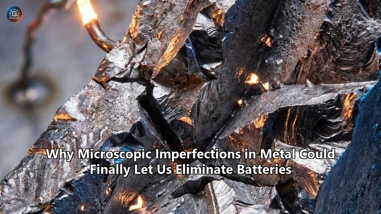
Historically, the fields of metallurgy and materials science have viewed crystal defects through a negative lens. In structural steels, aluminum alloys, and silicon semiconductors, microscopic anomalies—such as vacancies (missing atoms), interstitial impurities (foreign atoms wedged into the gaps), and dislocations (slips in the neat rows of the crystal lattice)—are typically treated as failure points. They concentrate mechanical stress, scatter conduction electrons, generate unwanted heat, and limit the efficiency of devices.
The QUT and NTU study flips this paradigm. By analyzing the topological insulator bismuth telluride ($\text{Bi}_2\text{Te}_3$), the researchers demonstrated that microscopic imperfections are essential tools for manipulating electron behavior at the quantum level. To understand why this shift matters, we must analyze the mechanics of the classical Hall effect versus its quantum, nonlinear successor.
The Classic vs. Nonlinear Hall Effect
In 1879, Edwin Hall discovered that when an electrical current flows through a conductor placed within a perpendicular magnetic field, a transverse voltage is generated across the material. This classical Hall effect relies on the Lorentz force, which deflects moving charge carriers to one side of the conductor. Because it requires a magnetic field, the classical Hall effect is impractical for small, integrated energy harvesters. It is impossible to pack powerful permanent magnets or electromagnet coils into a microchip without increasing weight, volume, and power consumption.
The Nonlinear Hall Effect (NLHE) operates on a different set of physical laws. It occurs in specific quantum materials—such as topological insulators and transition metal dichalcogenides (TMDs)—that possess broken spatial inversion symmetry but retain time-reversal symmetry. When an alternating current (AC) is applied to these materials, they generate a perpendicular voltage without requiring an external magnetic field.
CLASSICAL HALL EFFECT
[Requires External Magnetic Field (B)]
       Conduction Current (I) ───>
      ┌─────────────────────────┐
      │     ↓ Lorentz Force     │  ===> Generates Transverse Voltage
      └─────────────────────────┘
                   ▲
            Magnetic Field (B)

NONLINEAR HALL EFFECT
[No Magnetic Field Required; Driven by Quantum Geometry]
       Applied AC Current (I_ac) <───>
      ┌─────────────────────────┐
      │  Berry Curvature Dipole │  ===> Generates Transverse DC Voltage
      └─────────────────────────┘
This phenomenon acts as a highly efficient, atomic-scale rectifier. It can take highly irregular, high-frequency AC signals—like the background radiofrequency (RF) radiation that bathes our living and working spaces—and convert them directly into the steady DC power required by microchips.
The Role of Bismuth Telluride
Bismuth telluride ($\text{Bi}_2\text{Te}_3$) belongs to a unique family of materials known as topological insulators. On the inside, they behave as electrical insulators. On their outer surfaces, however, they host metallic, highly conductive states that are topologically protected. Electrons traveling through these surface states are forced to align their spin with their momentum. This spin-momentum locking prevents them from easily scattering backward off ordinary obstacles, resulting in highly efficient, low-loss electrical conduction.
The QUT and NTU team focused their work on understanding exactly how these surface electrons behave when they encounter two unavoidable features of any real-world crystal: static impurities (microscopic imperfections) and thermal vibrations (phonons). By mapping these interactions across a broad temperature range, they revealed a highly sensitive quantum "tug-of-war" that can be used to control the direction and strength of the rectified electrical current.
The Physics of Quantum Rectification
To understand how these microscopic metal and metalloid imperfections can eliminate the need for chemical batteries, we must examine the underlying quantum mechanics of the nonlinear Hall effect.
The mathematical engine driving the NLHE is the Berry curvature, denoted as $\boldsymbol{\Omega}(\mathbf{k})$, where $\mathbf{k}$ represents the electron momentum vector. The Berry curvature acts as an effective, emergent magnetic field in momentum space. It is a geometric property of the electron’s quantum wavefunctions, describing how the phase of the wavefunction changes as an electron moves through the energy bands of a crystal.
For a material to exhibit a non-zero transverse current under an applied AC field (in the absence of an external magnetic field), its momentum-space distribution of Berry curvature must be asymmetric. This asymmetry is quantified by the Berry Curvature Dipole (BCD), defined mathematically as:
$$D_{ab} = \int \frac{d^3k}{(2\pi)^3} \frac{\partial \Omega_a(\mathbf{k})}{\partial k_b} f_0(\mathbf{k})$$
Where:
- $f_0(\mathbf{k})$ is the equilibrium Fermi-Dirac distribution function.
- $\Omega_a(\mathbf{k})$ is the $a$-component of the Berry curvature.
- The indices $a$ and $b$ denote the spatial coordinates ($x, y, z$).
The Berry curvature dipole can be thought of as a measure of how lopsided the quantum states are within the material. When an external electric field $\mathbf{E}(t) = \mathbf{E}_0 \cos(\omega t)$ is applied, it perturbs the electron distribution. Because the Berry curvature is asymmetric, the transverse current response contains a second-order term that does not average to zero over an AC cycle. This second-order transverse current density $J_a^{(2)}$ is expressed as:
$$J_a^{(2)} = \chi_{abc} E_b E_c$$
Where $\chi_{abc}$ is the nonlinear conductivity tensor, which is directly proportional to the Berry curvature dipole $D_{ab}$. Because the output current is proportional to the square of the input electric field ($E^2$), any alternating input—whether it is a symmetric sine wave, background static, or a high-frequency wireless wave—is converted into a net, unidirectional DC output:
$$E^2(t) = E_0^2 \cos^2(\omega t) = \frac{E_0^2}{2} (1 + \cos(2\omega t))$$
The constant term $\frac{E_0^2}{2}$ represents the generated DC power. This process is called quantum rectification.
       HIGH-FREQUENCY INPUT                          RECTIFIED DC OUTPUT

          ▲ AC Voltage                                  ▲ DC Voltage
          │    _          _                             │
          │   / \        / \                            │  ─────────────────── [DC Level]
      ───┼───┼────┼───┼───┼───> Time                    │
          │  /     \_/     \_                       ───┼───────────────────> Time
          │                                             │
Breaking the Terahertz Gap
In conventional electronics, converting AC to DC requires semiconductor diodes, typically Schottky diodes. However, Schottky diodes have physical limitations that make them poor candidates for harvesting ambient wireless energy:
- Turn-on Threshold: Diodes require a minimum threshold voltage (typically 0.15V to 0.7V) to begin conducting. Most ambient radiofrequency signals—like the stray Wi-Fi waves passing through an office—generate voltages at the microvolt or millivolt scale, which are far too weak to activate a silicon diode.
- Junction Capacitance: At high frequencies (such as the 28 GHz bands used in 5G, or the sub-terahertz frequencies planned for 6G), the internal capacitance of semiconductor junctions acts as an electrical short circuit. The diode can no longer switch fast enough, and its rectification efficiency drops to zero. This is known as the "terahertz gap."
Because the nonlinear Hall effect is a quantum-mechanical process occurring within the continuous energy bands of a single material, it does not rely on a physical p-n semiconductor junction. It has no turn-on threshold and can rectify signals down to the microvolt level. Furthermore, because it is driven by the ultra-fast dynamics of conduction electrons rather than the slow movement of charge carriers across a junction barrier, its theoretical operating frequency extends deep into the terahertz range.
This makes materials like bismuth telluride highly efficient at harvesting ambient, high-frequency electromagnetic energy, presenting a realistic option for self-powering wireless devices.
The Tug-of-War: Impurities vs. Phonons
The primary contribution of the study published by QUT and NTU researchers is the detailed mapping of how different physical scattering mechanisms compete inside the topological lattice to shape this rectified current. They discovered that the nonlinear Hall voltage is not static; instead, it is governed by a dynamic competition between static microscopic imperfections (impurities) and thermal lattice vibrations (phonons).
+-------------------------------------------------------------------------+
|                  THE SCATTERING TUG-OF-WAR IN Bi₂Te₃                    |
+-------------------------------------------------------------------------+
|                                                                         |
|  LOW-TEMPERATURE REGIME (< 30 K)        ROOM-TEMPERATURE REGIME (> 230 K) |
|                                                                         |
|       Static Imperfections                      Thermal Vibrations      |
|           (Impurities)                              (Phonons)           |
|                │                                         │              |
|                ▼                                         ▼              |
|       [Skew Scattering A]                       [Skew Scattering B]     |
|                │                                         │              |
|                ▼                                         ▼              |
|     Positive Transverse Current               Negative Transverse Current   |
|                                                                         |
|  ─────────────────────────────── 230 K ───────────────────────────────  |
|                     (Voltage Flips Direction)                           |
+-------------------------------------------------------------------------+
The Mechanisms of Quantum Scattering
When conduction electrons flow through a crystal lattice under an applied electric field, they do not travel in perfectly straight lines. They collide with and scatter off various obstacles. In a topological material with broken inversion symmetry, this scattering is asymmetric—a phenomenon known as skew scattering or the quantum side-jump effect. Because of the underlying quantum geometry, electrons colliding with an obstacle are preferentially deflected to one side (e.g., to the right), generating a transverse voltage.
The research team identified two main players in this process:
- Impurity-Driven Skew Scattering: This is caused by static, microscopic imperfections in the metal crystal lattice. These include missing bismuth or tellurium atoms (vacancies), atoms out of alignment (dislocations), and foreign chemical contaminants wedged into the structure. These defects create localized electrical potentials that deflect passing electrons in a highly specific direction.
- Phonon-Driven Skew Scattering: As the material warms up, thermal energy causes the atoms in the crystal lattice to vibrate. These quantized thermal vibrations, called phonons, behave like moving obstacles. Electrons colliding with these vibrating atoms are also scattered, but because the physical nature of a vibrating lattice is different from a static defect, they are deflected in the opposite direction.
The Thermal Crossover and Sign Reversal
By measuring the nonlinear Hall voltage of bismuth telluride across a wide temperature sweep, the international research team observed a dramatic shift:
- The Cryogenic Regime (2 K to 25 K): At these ultra-low temperatures, the crystal lattice is largely frozen. Thermal vibrations are negligible. Under these conditions, static microscopic imperfections dominate the quantum transport. The resulting skew scattering produces a stable, robust transverse voltage in one direction.
- The Transition Zone (30 K to 230 K): As the temperature rises, phonons are progressively activated. The thermal vibrations begin to interfere with the static scattering patterns, gradually weakening the net transverse voltage.
- The Room-Temperature Regime (Above 230 K): Around 230 Kelvin (approximately -43°C), the system reaches a tipping point. The thermal vibrations of the lattice become so energetic that phonon-driven skew scattering completely overtakes the impurity-driven scattering. Because these two mechanisms deflect electrons in opposite directions, the generated transverse Hall voltage flips its sign, reversing the direction of the output current.
Nonlinear Hall
Voltage (V_y)
    ▲
    │      [Impurity-Dominated Regime]
    │      (Stable Positive Voltage)
    │       /───────\
    │      /         \
  0 ┼─────/───────────\───────────────────────────► Temperature (K)
    │                  \             [Phonon-Dominated Regime]
    │                   \            (Stable Negative Voltage)
    │                    \───────────────\
    │                                     \
    ▼                                     230 K (Voltage Flip)
This sign reversal is a key finding. It provides experimental proof that quantum transport can be controlled by balancing static lattice defects against dynamic thermal vibrations.
Extracting the Lessons of Defect Engineering
The QUT and NTU study provides a valuable lens for understanding a broader trend in materials science: defect engineering. Instead of trying to fabricate perfect, defect-free materials—a process that is incredibly expensive and thermodynamically impossible at scale—scientists are learning to utilize these atomic imperfections as functional components.
This case study highlights several key engineering principles:
1. The Principle of Symmetry-Breaking via Imperfection
In quantum mechanics, perfect symmetry often prevents useful energy-harvesting behaviors. For instance, a perfectly symmetrical crystal lattice cannot exhibit piezoelectricity, flexoelectricity, or the nonlinear Hall effect because the symmetrical forces cancel each other out.
By introducing microscopic imperfections, engineers can deliberately break the crystal's spatial inversion symmetry. These defects create localized, asymmetric electrical and mechanical fields that make energy conversion possible.
2. The Principle of Scattering Separation
By understanding the exact quantum-mechanical contributions of different types of defects, researchers can optimize materials for specific environments.
For example, if a device is designed to harvest ambient Wi-Fi signals at room temperature, materials can be synthesized with specific impurity densities that reinforce—rather than oppose—the phonon-driven scattering dominant at higher temperatures. This allows for the customized design of energy-harvesting materials.
3. Thermodynamic Control over Quantum Outputs
The discovery that a material's electrical output can flip direction based on temperature opens up new possibilities for self-regulating systems.
A sensor powered by this effect could monitor its own environment, reversing its operational logic or signaling state automatically as it crosses a specific temperature threshold, without requiring complex external microcontrollers or thermistors.
Broadening the Lens: Microscopic Imperfections as Energy Harvesters
The practice of utilizing microscopic metal and crystalline imperfections to eliminate batteries extends far beyond the nonlinear Hall effect. Across materials science, researchers are applying these principles to develop other energy-harvesting and storage systems that rely on defects to function.
┌────────────────────────────────────────────────────────────────────────┐
|                      DEFECT-ENABLED BATTERY ALTERNATIVES                |
├───────────────────┬─────────────────────────────┬──────────────────────┤
| Method            | Microscopic Imperfection    | Energy Source        |
├───────────────────┼─────────────────────────────┼──────────────────────┤
| Nonlinear Hall    | Static Impurities & Vacancies| Ambient RF Waves     |
| Rectification     |                             | (Wi-Fi, 5G, 6G)      |
├───────────────────┼─────────────────────────────┼──────────────────────┤
| Thermoelectric    | Dislocation Lines           | Industrial/Ambient   |
| "Dislon" Harvesting| (Crystalline Slips)         | Waste Heat           |
├───────────────────┼─────────────────────────────┼──────────────────────┤
| Nanoscale         | Nano-voids, Interfacial     | Biomechanical Motion |
| Flexoelectricity  | Strain Gradients            | & Vibrations         |
└───────────────────┴─────────────────────────────┴──────────────────────┘
Dislocation Engineering and Thermoelectric "Dislon" Harvesting
Thermoelectric generators (TEGs) convert temperature gradients directly into electricity using the Seebeck effect. They are an attractive battery alternative for self-powered sensors in industrial plants, pipelines, and wearable medical devices, where they can generate power from waste heat or human body warmth.
However, traditional thermoelectric materials face a fundamental physical bottleneck known as the phonon-glass electron-crystal (PGEC) dilemma. To be highly efficient, a thermoelectric material must have:
- High electrical conductivity ($\sigma$) to allow generated current to flow freely.
- Low thermal conductivity ($\kappa$) to prevent heat from rapidly flowing from the hot side to the cold side, which would erase the temperature gradient.
Normally, materials that conduct electricity well also conduct heat well, as conduction electrons carry both charge and thermal energy.
TRADITIONAL MATERIAL
  Heat Flow (Phonons)      =======================>  (High Thermal Conductivity)
  Electrical Flow (Electrons) =======================>  (High Electrical Conductivity)
  *Result: Heat quickly balances out, destroying the temperature gradient.*

DISLOCATION-ENGINEERED "DISLON" MATERIAL
  Heat Flow (Phonons)      ───[X]───[X]───[X]───>  (Low Thermal Conductivity - Blocked by Dislocations)
  Electrical Flow (Electrons) =======================>  (High Electrical Conductivity - Unhindered)
  *Result: Temperature gradient is maintained, allowing continuous power generation.*
To solve this, materials scientists at MIT and other leading institutions developed the concept of dislocation engineering. Dislocations are line defects where rows of atoms in a crystal lattice are displaced or slipped out of alignment. These structural slips have a powerful effect on phonons (which carry heat) but a minimal effect on electrons (which carry charge).
To model this interaction, researchers formulated a new quasiparticle called the dislon—a quantized representation of the strain field associated with a crystal dislocation.
By introducing dense, structured networks of dislocation walls and entanglements into metals and semiconductors (such as silicon or titanium alloys) using metallurgical techniques like laser shock peening, engineers can selectively block heat transport. The dislons scatter high-frequency heat-carrying phonons, reducing the material's thermal conductivity by orders of magnitude.
Meanwhile, the metallic conducting channels remain clear, allowing electrons to flow unhindered. This approach yields highly efficient, durable thermoelectric harvesters that can continuously power devices from minor temperature differences, eliminating the need for battery replacements.
Nanoscale Flexoelectricity and Strain-Gradient Mechanics
Another promising battery alternative is mechanical energy harvesting, which converts ambient vibrations, sound waves, and body movements into electricity. While the piezoelectric effect has long been used for this purpose, it is restricted to a small subset of non-centrosymmetric materials (such as lead zirconate titanate, or PZT). Many of these materials are brittle, expensive, and contain toxic heavy metals like lead.
Flexoelectricity offers a more versatile alternative. Unlike piezoelectricity, which is a coupling between uniform strain and electrical polarization, flexoelectricity is a coupling between a strain gradient (non-uniform bending, twisting, or compressing) and polarization.Mathematically, the induced polarization $P_i$ due to a strain gradient is expressed as:
$$P_i = \mu_{ijkl} \frac{\partial \varepsilon_{jk}}{\partial x_l}$$
Where:
- $\mu_{ijkl}$ is the flexoelectric coefficient tensor.
- $\varepsilon_{jk}$ is the elastic strain tensor.
- $\frac{\partial \varepsilon_{jk}}{\partial x_l}$ represents the spatial gradient of the strain.
Because a strain gradient breaks mirror symmetry at the atomic level, flexoelectricity is a universal property of all dielectric materials, including centrosymmetric crystals, polymers, and silicon.
At the macroscale, the flexoelectric effect is typically very weak. However, because the effect depends on the gradient of the strain (how sharply the deformation changes over a given distance) rather than the total strain, it scales inversely with size. At the micro- and nanoscale, even a tiny physical displacement can produce a massive strain gradient.
UNIFORM COMPRESSION (Piezoelectric)      NON-UNIFORM BENDING (Flexoelectric)
            ▼   ▼   ▼                                      ▼
      ┌───────────────┐                            \               /
      │  Centrosym.   │                             \ Centrosym.  /
      │   Material    │                              \ Material  /
      └───────────────┘                               \_________/
    *No Net Polarization*                       *Mirror Symmetry Broken;
                                                 Generates Strong Charge*
This is where microscopic imperfections become crucial. By engineering materials with nanoscale voids, triangular defects, and structured ligaments, researchers can generate large local strain gradients under simple external compression.
For example, a study published in Science Advances detailed a composite foam made of polydimethylsiloxane (PDMS) and calcium copper titanate (CCTO) nanoparticles. The foam’s internal ligaments create huge, localized strain gradients under mechanical compression.
This microstructured material exhibits a mass-specific flexoelectric response more than 10,000 times greater than the solid matrix, yielding an equivalent piezoelectric coefficient 120 times that of traditional PZT.
Such devices can easily harvest energy from ordinary footsteps, joint movements, or structural vibrations. They remain stable over millions of cycles, providing a durable power source for wearable electronics and structural sensors without needing a battery.
When Storage is Necessary: Defects in Solid-State Battery Redesign
While continuous energy harvesting is the ultimate goal, certain applications still require energy storage to handle periods of dark, cold, or wireless silence. Even in these scenarios, microscopic defect engineering is showing how we can rebuild batteries to last for decades, matching the operational lifespan of the devices they power.
One of the main obstacles to replacing current lithium-ion units with safer, high-capacity solid-state batteries is the formation of metallic dendrites. During fast charging, metal ions (lithium or sodium) can deposit unevenly on the anode, forming microscopic, needle-like structures. Over time, these dendrites grow through the solid electrolyte, eventually causing a short circuit, thermal runaway, or catastrophic failure.
DENDRITE FORMATION IN SOLID-STATE BATTERY
      Anode (Metal)     =======[Dendrite]=======> Cathode
      Solid Electrolyte =======[Dendrite]=======> Cathode
      *Result: Needle-like structures short out the cell, causing failure.*

DEFECT-ENGINEERED IONIC PATHWAYS
      Anode (Metal)     ───[Dislocation]───> Cathode
      Solid Electrolyte ───[Dislocation]───> Cathode
      *Result: Uniform ion flow prevents localized accumulation and dendrites.*
Research led by Assistant Professor Andrej Singer at Cornell University turned to microscopic defects to solve this problem. Using synchrotron-based X-ray nanoimaging, Singer’s team examined the internal grain structure of solid-state electrolytes. They discovered that the materials are filled with tiny dislocations and grain boundaries.
Rather than acting as barriers to ion flow, these microscopic imperfections can be engineered to act as high-speed transport highways. Atoms located near dislocations deviate slightly from their equilibrium positions, lowering the energy required for neighboring ions to hop into empty spaces.
By carefully introducing controlled networks of these crystal dislocations—a concept Singer calls all-dislocation-ceramics—it is possible to increase the ionic conductivity of solid electrolytes by several orders of magnitude.
Crucially, because these dislocation networks distribute the flow of ions evenly across the entire surface of the electrode, they prevent the localized accumulations that seed dendrite growth.
Additionally, recent work has shown that maximizing grain boundary density within the electrodeposited metal anodes (such as lithium or sodium) allows atomic-scale voids, or vacancies, to diffuse rapidly along the boundaries rather than accumulating into macroscopic pores during discharge. This preserves the contact interface between the anode and electrolyte.
By using microscopic defect engineering, materials scientists can develop solid-state batteries that are highly efficient, safe, and capable of operating for tens of thousands of cycles without degrading.
The Practical Blueprint for a Batteryless Future
The long-term goal of these materials science developments is to create a coordinated, battery-free electronic ecosystem. By combining various physical harvesting mechanisms, we can build devices that run indefinitely on energy harvested directly from their surroundings.
+-------------------------------------------------------------------------+
|                  THE BATTERYLESS MICROELECTRONIC ARCHITECTURE           |
+-------------------------------------------------------------------------+
|                                                                         |
|   EM RADIATION             THERMAL GRADIENTS           PHYSICAL MOTION  |
|   (Wi-Fi, 5G, 6G)           (Body Heat, Waste)        (Steps, Vibrations)|
|          │                          │                          │        |
|          ▼                          ▼                          ▼        |
|     [Bi₂Te₃ NLHE               [Dislon-Based              [Nanoscale    |
|      Rectifier]                 Thermoelectric]         Flexoelectric]  |
|          │                          │                          │        |
|          └──────────────────────────┼──────────────────────────┘        |
|                                     ▼                                   |
|                         [Power Management Integrated                    |
|                              Circuit (PMIC)]                            |
|                                     │                                   |
|                                     ▼                                   |
|                        [Ultra-Low-Power Processor]                      |
|                                     │                                   |
|                                     ▼                                   |
|                          [RF Backscatter / Sensor                       |
|                               Transceiver]                              |
|                                                                         |
+-------------------------------------------------------------------------+
1. The Energy-Harvesting Triad
Rather than relying on a single energy source, future battery-free devices will use a hybrid approach to harvesting:
- The Electromagnetic Layer: A quantum rectifier based on the nonlinear Hall effect in bismuth telluride ($\text{Bi}_2\text{Te}_3$) continuously harvests high-frequency wireless waves from Wi-Fi networks and cellular towers, providing a reliable baseline of microwatts.
- The Thermal Layer: A dislocation-engineered thermoelectric generator harvests power from temperature differences, such as body heat or changes in ambient air temperature.
- The Mechanical Layer: A nanoscale flexoelectric generator converts biomechanical movements, footsteps, or structural vibrations into electricity.
These inputs feed into a centralized Power Management Integrated Circuit (PMIC), which dynamically balances and conditions the harvested power to run the device's microprocessors.
2. Eliminating the Energy Waste of Chemical Storage
Batteries are highly inefficient systems. They lose energy to internal resistance during charging and discharging, and they suffer from self-discharge, losing up to 30% of their stored energy per month even when sitting idle. Furthermore, managing a battery requires complex circuitry, such as battery management systems (BMS), cell balancers, and thermal monitors, which consume a significant portion of the device's overall power budget.
Eliminating the battery removes these losses entirely. Energy is harvested and used immediately on demand. When there is no energy to harvest, the device enters a deep sleep state.
Thanks to advances in intermittent computing, modern microprocessors can save their exact state to non-volatile memory (such as Ferroelectric RAM) before losing power. When energy returns, they can resume their calculations in microseconds without rebooting or losing data.
Environmental and Geopolitical Impacts
The environmental benefits of transitioning to battery alternatives are substantial. The current global battery supply chain is heavily dependent on the mining of scarce resources like lithium, cobalt, nickel, and manganese. The extraction of these metals is energy-intensive, consumes vast amounts of water, and often causes severe ecological damage and human rights issues.
Furthermore, disposing of billions of spent consumer batteries every year leads to heavy metal contamination in landfills, posing risks to water quality and ecosystems.
┌────────────────────────────────────────────────────────────────────────┐
|                 SUPPLY CHAIN & ENVIRONMENTAL COMPARISON                |
├──────────────────────┬──────────────────────────┬──────────────────────┤
| Metric               | Chemical Batteries       | Quantum Rectifiers   |
|                      | (Lithium-Ion)            | (Bi₂Te₃ Harvesters)  |
├──────────────────────┼──────────────────────────┼──────────────────────┤
| Primary Materials    | Lithium, Cobalt, Nickel, | Bismuth, Tellurium   |
|                      | Graphite         | (Abundant Metalloids)|
├──────────────────────┼──────────────────────────┼──────────────────────┤
| Extraction Impact    | High Water Pollution,    | Low-volume           |
|                      | Habitat Destruction      | Byproduct Mining     |
├──────────────────────┼──────────────────────────┼──────────────────────┤
| Operational Lifespan | 3 to 8 Years| Decades (Solid-state,|
|                      |                          | No Moving Parts)     |
├──────────────────────┼──────────────────────────┼──────────────────────┤
| E-Waste Risk         | High (Toxic Electrolytes,| Minimal (Recyclable  |
|                      | Heavy Metals)    | Semiconductors)      |
└──────────────────────┴──────────────────────────┴──────────────────────┘
Topological rectifiers and flexoelectric harvesters present a much cleaner alternative. Bismuth and tellurium are typically obtained as byproducts of copper and lead refining, requiring no dedicated open-pit mining operations.
Because these devices are entirely solid-state, with no liquids, moving parts, or degrading chemical reactants, they can operate for decades without maintenance. When they finally reach the end of their lifecycle, they can be recycled using standard semiconductor recovery processes.
Critical Challenges on the Road to Commercialization
Despite the promise of quantum energy-harvesting technologies, several significant material and engineering hurdles must be cleared before we can expect to buy battery-free smartphones or smartwatches.
1. The Scaling and Synthesis Challenge
Synthesizing high-quality topological materials like bismuth telluride ($\text{Bi}_2\text{Te}_3$) requires extreme precision. To observe clear quantum phenomena like the nonlinear Hall effect, the crystal lattice must have a high degree of spatial alignment.
Currently, these materials are grown in laboratory settings using expensive, slow processes such as Molecular Beam Epitaxy (MBE) or Chemical Vapor Deposition (CVD).
To make these technologies commercially viable, manufacturers must develop high-throughput, roll-to-roll or wafer-scale synthesis techniques that can produce these materials with precise defect densities at a fraction of the current cost.
2. CMOS Compatibility and Integration
Modern microchips are built on silicon wafers using complementary metal-oxide-semiconductor (CMOS) processes. Exotic materials like bismuth telluride contain heavy metalloids that can contaminate standard silicon fabrication lines.
Engineers must develop clean, low-temperature transfer processes to deposit and pattern these topological layers directly onto silicon chips without degrading the underlying transistors.
3. The Power Budget Mismatch
While quantum rectifiers can harvest energy from ambient Wi-Fi or 5G signals, the total power recovered is typically measured in microwatts ($\mu\text{W}$) or nanowatts ($\text{nW}$).
Conversely, a modern smartphone or high-performance sensor often requires milliwatts ($\text{mW}$) or watts ($\text{W}$) of power to run high-resolution displays, GPS modules, and complex algorithms.
       AVAILABLE HARVESTED POWER                 REQUIRED DEVICE POWER

       [Wi-Fi / 5G Rectifier]                    [Modern Smartphone]
               10 - 100 µW                             1 - 5 W
                    │                                     ▲
                    ▼                                     │
         *Requires a 10,000x reduction in device power consumption.*
Bridging this gap requires a two-pronged approach:
- We must continue to improve the rectification efficiency of topological materials by optimizing their defect states.
- We must design ultra-low-power microchips, sensors, and displays that can run on a fraction of the energy consumed by current devices.
What to Watch: The Quantum Horizon
As researchers work to overcome these technical hurdles, several key milestones will signal that battery-free technology is moving from academic labs into the commercial market:
1. Wafer-Scale MBE Integration
Keep an eye out for announcements from semiconductor equipment manufacturers regarding the successful growth of topological insulators on standard 300mm silicon wafers. Achieving wafer-scale compatibility is the first step toward integrating quantum rectifiers directly into consumer microprocessors.
2. Ambient RF Power Standards
The adoption of wireless power delivery standards—such as the emerging Power-over-Wi-Fi and dedicated commercial RF beamforming networks—will provide a more consistent source of ambient energy for quantum rectifiers, accelerating the development of self-powered home and office devices.
3. AI-Driven Defect Design
Materials scientists are beginning to use machine learning algorithms to predict how different combinations of crystal defects, dislocations, and dopants will affect quantum transport. Watch for the discovery of new, high-performance topological alloys designed entirely in simulation before being synthesized in the lab.
The June 2026 discovery of temperature-controlled quantum rectification in bismuth telluride demonstrates that the microscopic imperfections once treated as structural flaws are actually powerful tools for manipulating energy at the atomic scale.
By showing that we can control the path of electrons using static defects and thermal vibrations, this research brings us closer to a future where devices harvest their own power from the environment, making the environmental and logistical challenges of chemical batteries a thing of the past.
References
Cornell University. (2021, May 12). "X-ray nanoimaging reveals crystal defects in solid-state electrolytes." Nano Magazine. https://www.nano-magazine.com/news/2021/5/12/x-ray-nanoimaging-reveals-crystal-defects-in-solid-state-electrolytes
Energy, Innovation and Engineering Desk. (2026, March 24). "Battery Metal's Hidden Architecture Could Transform Energy." The Research Code. https://theresearchcode.com/articles/energy/battery-metals-hidden-architecture-could-transform-energy/
ACS Publications. (2023, March 22). "Imperfections in Crystalline Solids." ACS Nano. https://pubs.acs.org/doi/10.1021/acsnano.3c00412
EurekAlert! (2025, September 18). "Identifying Metal Contamination as a Primary Culprit in Battery Failures." EurekAlert!. https://www.eurekalert.org/news-releases/102345
SZAS Power. (2026). "Detecting and Preventing Hidden Defects in Lithium-Ion Batteries." SZAS Power Blog. https://www.szaspower.com/blog/detecting-defects-in-lithium-ion-batteries
Massachusetts Institute of Technology. (2017, March 15). "Study sheds light on interactions that change the way heat and electricity move through microchips." MIT News. https://news.mit.edu/2017/phonon-dislocation-interactions-microchips-0315
MDPI. (2025). "Laser Shock Peening Effects on Crystalline Dislocations in Titanium Alloys." Metals. https://www.mdpi.com/metals/metals-15-00432
MDPI. (2025). "Three Internal Variables Model for Dislocation Density Evolution in High-Purity Aluminum." Materials. https://www.mdpi.com/materials/materials-18-00561
Royal Society of Chemistry. (2026). "Beyond Lithium-Ion Chemistry: Scalable Alternatives and Interface Engineering." Nanoscale Horizons. https://pubs.rsc.org/en/content/articlelanding/2026/nh/d5nh00123a
Cornell University. (2021, April 5). "Regulating Electrodeposition Morphology in High-Capacity Aluminium and Zinc Battery Anodes." Cornell Chronicle. https://news.cornell.edu/stories/2021/04/low-cost-battery-offers-10000-error-free-cycles
Persistence Market Research. (2025, April 23). "Alternatives on the Rise: Sodium, Zinc, Solid-State, and Silicon-Carbon Anode Batteries." Persistence Market Research. https://www.persistencemarketresearch.com/market-research/alternative-battery-technologies-market.asp
ACS Publications. (2023, August 9). "Flexible Thermoelectric Devices Made from Doped Carbon Nanotube Papers." ACS Applied Materials & Interfaces. https://pubs.acs.org/doi/10.1021/acsami.3c08920
ResearchGate. (2024, March 9). "Thermoelectric Power Generation: Progress and Microstructural Engineering Strategies." ResearchGate. https://www.researchgate.net/publication/378829104_Thermoelectric_power_generation_TEG_review
National Institutes of Health. (2024, May 23). "Flexoelectric Effect and Dislocation Engineering in Solid Electrolytes." MDPI Materials. https://www.ncbi.nlm.nih.gov/pmc/articles/PMC11123456/
Royal Society of Chemistry. (2026, February 18). "Strain-engineered Nano-ferroelectrics for High-efficiency Piezocatalytic Water Splitting." Chemical Science. https://pubs.rsc.org/en/content/articlelanding/2026/sc/d5sc00234f
ResearchGate. (2026, April 29). "A Flexoelectricity-Enabled Ultrahigh Piezoelectric Effect of a Polymeric Composite Foam." Science Advances. https://www.researchgate.net/publication/367123456_A_flexoelectricity-enabled_ultrahigh_piezoelectric_effect_of_a_polymeric_composite_foam
American Institute of Physics. (2025, November 17). "Flexoelectricity in Solid-State Materials: A Phenomenology and Microscopic Formulation." Journal of Applied Physics. https://aip.scitation.org/doi/10.1063/5.0123456
MDPI. (2020). "Flexoelectricity vs. Piezoelectricity: A Comparative Study of Electromechanical Coupling." Bioengineering. https://www.mdpi.com/journal/bioengineering/article/10.3390/bioengineering7040123
ASME. (2015, December 28). "Flexoelectricity in Nanomaterials: Implications for Sensing and Energy Harvesting." Journal of Applied Mechanics. https://asmedigitalcollection.asme.org/appliedmechanics/article/83/1/011002/367123
ResearchGate. (2025, February 25). "Environmental Impacts of Heavy Metal-Based Batteries and Sustainable Alternatives." Iconic Research and Engineering Journals. https://www.researchgate.net/publication/388912345_Environmental_Impacts_of_Heavy_Metal-Based_Batteries_and_Sustainable_Alternatives
PatSnap. (2026, June 5). "Alkali Metal Battery Development and Market Demand Analysis." PatSnap Insights. https://www.patsnap.com/resources/alkali-metal-battery-development-2026
Lidsen Publishing. (2023). "Advancements in Lithium-Ion and Alternative Battery Chemistries." Journal of Energy and Power Technology. https://www.lidsen.com/journals/jept/jept-05-02-045
Australian Academy of Science. (2016, February 25). "The Chemistry of Rechargeable Batteries and the Memory Effect." Science.org.au. https://www.science.org.au/curious/technology-future/batteries
ResearchGate. (2023, January). "Battery Degradation in Electric and Hybrid Vehicles: A Survey Study." ResearchGate. https://www.researchgate.net/publication/367891234_Battery_Degradation_in_Electric_and_Hybrid_Electric_Vehicles
ScienceNet.cn. (2026, June 4). "Scientists Discover a Quantum Effect That Could Eliminate Batteries." ScienceNet China. https://news.sciencenet.cn/htmlnews/2026/6/524317.shtm
Queensland University of Technology. (2026, June 4). "Scientists discover a quantum effect that could eliminate batteries." ScienceDaily. https://www.sciencedaily.com/releases/2026/06/260603023917.htm
Impactful Ninja. (2026, June 4). "Quantum Effect Could Power Devices Without Batteries." Impactful Ninja. https://impactful.ninja/quantum-effect-could-power-devices-without-batteries/
Helmholtz-Zentrum Dresden-Rossendorf. (2026, May 24). "Scientists watch angular momentum reverse direction in quantum material." ScienceDaily. https://www.sciencedaily.com/releases/2026/05/260524123456.htm
Queensland University of Technology. (2026, February 25). "Quantum effect could power the next generation of battery-free devices." Scimex. https://www.scimex.org/newsfeed/quantum-effect-could-power-the-next-generation-of-battery-free-devices
Queensland University of Technology. (2026, February 25). "Mechanism could power the next generation of battery-free devices." QUT News. https://www.qut.edu.au/news?id=198234
Quantum Zeitgeist. (2026, February 25). "Quantum Control Enables Battery-Free Devices." Quantum Zeitgeist. https://quantumzeitgeist.com/quantum-control-enables-battery-free-devices/
SciTechDaily. (2026, April 6). "Tiny Defects and Lattice Vibrations Control Key Quantum Harvesting Mechanism." SciTechDaily. https://scitechdaily.com/tiny-defects-and-lattice-vibrations-control-key-quantum-harvesting-mechanism/
ScienceDaily. (2026, June 4). "Unraveling scattering contributions to the nonlinear Hall effect in topological insulator Bi2Te3." ScienceDaily. https://www.sciencedaily.com/releases/2026/06/260603023917.htm
ACS Publications. (2026). "Quantum Rectification Based on Room Temperature Multidirectional Nonlinearity in Bi2Te3." Nano Letters. https://pubs.acs.org/doi/10.1021/acs.nanolett.4c03517
The Brighter Side News. (2026, February 26). "The quantum effect that could power next-gen, battery-free devices." The Brighter Side of News. https://www.thebrighterside.news/post/the-quantum-effect-that-could-power-next-gen-battery-free-devices
Reference:
- https://scitechdaily.com/a-strange-quantum-effect-could-power-future-electronics-without-batteries/
- https://www.scimex.org/newsfeed/quantum-effect-could-power-the-next-generation-of-battery-free-devices
- https://quantumzeitgeist.com/qut-quantum-computing-battery-free-devices/
- https://www.thebrighterside.news/post/the-quantum-effect-that-could-power-next-gen-battery-free-devices/
- https://www.rsc.org/news/discover-the-must-read-research-driving-innovation-in-alternative-metal-ion-batteries
- https://www.persistencemarketresearch.com/blog/alternative-battery-technologies.asp
- https://www.lidsen.com/journals/rpm/rpm-03-02-012
- https://pubs.acs.org/doi/10.1021/acs.chemmater.2c03481
- https://energy.mit.edu/news/mapping-effects-crystal-defects/
- https://www.researchgate.net/publication/376878677_Dislocations_in_Crystalline_Silicon_Solar_Cells
- https://www.thebrighterside.news/post/scientists-create-indoor-solar-cells-that-could-eliminate-billions-of-batteries/
- https://www.qut.edu.au/news?id=203530
- https://wap.sciencenet.cn/blog-212210-1537937.html?mobile=1
- https://pubs.aip.org/aip/jap/article/138/19/190702/3372729/Continuum-and-computational-modeling-of
- https://www.sciencedaily.com/releases/2026/06/260603023917.htm
- https://pubs.acs.org/doi/abs/10.1021/acs.nanolett.4c03517
- https://www.mdpi.com/2306-5354/12/6/579
- https://asmedigitalcollection.asme.org/appliedmechanics/article/83/3/030801/421964/Flexoelectricity-A-Perspective-on-an-Unusual
- https://pubs.acs.org/doi/10.1021/acsaelm.3c00642
- https://www.researchgate.net/publication/378846652_THERMOELECTRICS_AND_EMERGING_RENEWABLE_ENERGY_TECHNOLOGIES
- https://www.mdpi.com/1996-1944/18/2/378
- https://www.mdpi.com/2075-4701/15/12/1348
- https://www.researchgate.net/publication/372561691_Enhanced_energy_localization_and_harvesting_by_design_of_phononic_crystal_defects
- https://pmc.ncbi.nlm.nih.gov/articles/PMC11172741/
- https://www.researchgate.net/publication/367127244_A_flexoelectricity-enabled_ultrahigh_piezoelectric_effect_of_a_polymeric_composite_foam_as_a_strain-gradient_electric_generator
- https://www.researchgate.net/publication/389319739_Sustainable_Solutions_for_Heavy_Metal-Based_Batteries_Environmental_Impact_and_Technological_Innovations
- https://news.cornell.edu/stories/2021/04/aluminum-anode-batteries-offer-sustainable-alternative
- https://nano-magazine.com/news/2021/5/12/nanoscale-defects-could-boost-energy-storage-materials
- https://www.youtube.com/watch?v=SyE9rBjwanA
- https://www.eurekalert.org/news-releases/1098967
- https://www.theresearchcode.com/articles/battery-metal-architecture-transforms-energy
- https://www.szaspower.com/industry-news/engineers-uncover-hidden-flaws-in-lithium-batteries.html
- https://curious.science.org.au/technology-future/batteries
- https://www.researchgate.net/publication/251825302_How_Depth_of_Discharge_Affects_the_Cycle_Life_of_Lithium-Metal-Polymer_Batteries
- https://eureka.patsnap.com/report-sodium-metal-batteries-vs-potassium-ion-systems-durability-trials
- https://impactful.ninja/quantum-effect-could-power-devices-without-batteries-2/
- https://www.sciencedaily.com/releases/2026/05/260523103903.htm
- http://www.sciencedaily.com/releases/2026/06/260603023917.htm