
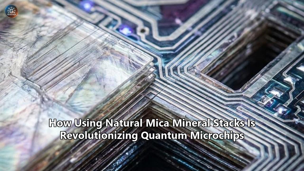
A major obstacle in solid-state quantum hardware has met an unexpected solution from economic geology. An international research team led by the University of Southampton and the National University of Singapore (NUS) has unveiled a clean manufacturing method for two-dimensional (2D) quantum microchips by substituting synthetic polymers with natural muscovite mica mineral stacks.
The study, published in Nature Communications, details how inorganic muscovite crystals eliminate microscopic organic contamination during the assembly of atomically thin van der Waals (vdW) heterostructures. By providing an atomically flat, inorganic platform for layer stacking, the process unlocks precise angle-controlled alignment in 2D materials like graphene, hexagonal boron nitride (hBN), and transition metal dichalcogenides (TMDs). This mechanical alignment induces exotic quantum phenomena—including room-temperature topological states, magic-angle superconductivity, and tunable quantum magnetism—without the signal-degrading organic residues left behind by traditional manufacturing stamps.
+-----------------------------------------------------------------------------------+
|                           2D MATERIALS TRANSFER METHODS                           |
+------------------------------------+----------------------------------------------+
| CONVENTIONAL POLYMER STAMPING      | NATURAL MICA MINERAL STACKING                |
| (PMMA / PPC / PDMS)                | (Inorganic Muscovite Crystals)               |
+------------------------------------+----------------------------------------------+
| • Organic carbon residue at bounds | • Atomically pristine, residue-free contact  |
| • Polymer trapped air bubbles      | • Molecularly flat crystal cleavage planes   |
| • Mechanical strain & distortion   | • Rigid mechanical support during alignment  |
| • Thermal ceiling (~150°C)         | • High thermal stability (>500°C annealing)  |
| • Unpredictable twist-angle drift  | • Sub-0.05° precision twistronics control    |
+------------------------------------+----------------------------------------------+
"When 2D materials are stacked into layered structures with a controlled angle between the layers, they exhibit entirely new electronic properties," explained Dr. Makars Šiškins, Lecturer in Experimental Physics at the University of Southampton and lead author of the study. "Our new method allows us to precisely align the layers to create these complex structures that were previously too hard to make. This level of precision is vital for quantum material research, where even a tiny amount of contamination can obscure the results."
Co-lead author Prof. Alexey Berdyugin from the NUS Institute for Functional Intelligent Materials emphasized the structural advantage: "Because mica is an inorganic crystal, rather than a soft polymer, it avoids many of the contamination issues that plague conventional methods. It also produces ultra-clean surfaces, allowing electronic components to function at their full potential."
As quantum engineering transitions from experimental proof-of-concept devices to scalable, error-corrected microchips, this natural mica technique presents a direct challenge to existing solid-state fabrication pipelines. By examining competing hardware paradigms, processing tradeoffs, and supply chain dynamics, the integration of mica mineral quantum computing architecture highlights both distinct advantages and remaining industrial hurdles.
The Physics of Interfacial Pollution in Quantum Microchips
To understand why natural mica mineral stacks represent a critical shift in nanomanufacturing, one must look at the quantum physics governing van der Waals heterostructures.
Unlike bulk 3D semiconductors such as silicon or gallium arsenide, which rely on covalent or ionic atomic bonds, 2D heterostructures are formed by stacking single-atom-thick sheets held together by weak van der Waals forces. When two identical or dissimilar 2D lattices (such as two sheets of graphene or a layer of tungsten diselenide on hexagonal boron nitride) are placed atop one another at a specific rotation angle—a field known as twistronics—the overlapping atomic patterns form a moiré superlattice.
       [ Top 2D Layer (Graphene/TMD) ]  --> Twist Angle θ
   -----------------------------------------  <-- Interfacial Residue Trap
       [ Bottom 2D Layer / Substrate ]
This moiré superlattice alters the band structure of the material, flattening electronic energy bands and forcing electrons to interact strongly with one another. At specific magic angles (such as $1.1^\circ$ for bilayer graphene), electron kinetic energy drops to zero, giving rise to unconventional superconductivity, correlated insulating states, and spontaneous ferromagnetism.
However, these delicate quantum states are fragile. Conventional nanofabrication relies on polymer-assisted transfer techniques using compounds like polymethyl methacrylate (PMMA), polypropylene carbonate (PPC), or polydimethylsiloxane (PDMS). During assembly, a polymer film picks up an exfoliated 2D flake, positions it over a target substrate, and drops it down.
When the polymer is chemically dissolved away using solvents like acetone or chloroform, it leaves behind microscopic organic residues, hydrocarbon chains, and trapped atmospheric gas bubbles.
These contaminants introduce four catastrophic failure modes into quantum microchips:
- Charge Scattering and Dephasing: Organic residues act as localized charged impurities, creating random electrostatic potential fluctuations. These fluctuations scatter charge carriers, reducing electron mobility by orders of magnitude and shortening qubit coherence times ($T_1$ and $T_2$).
- Dielectric Loss and Two-Level Systems (TLS): Amorphous polymer carbon chains contain defects that act as microscopic electric dipoles. These two-level systems absorb microwave photons emitted by quantum circuits, causing rapid energy dissipation and decoherence.
- Local Strain and Lattice Distortion: Soft polymer stamps exert uneven lateral forces during release, introducing non-uniform physical strain into the 2D lattice. This strain disrupts the precise periodic potential of the moiré superlattice, destroying correlated electronic states.
- Twist Angle Inhomogeneity: Soft viscoelastic polymers shift during the transfer process, causing local twist angles to vary across a single microchip. A variation of just $0.05^\circ$ is sufficient to alter the material from a superconductor into a standard conductor.
+---------------------------------------------------------------------------------+
|               IMPACT OF INTERFACIAL RESIDUES ON QUANTUM STATES                  |
+------------------------------+--------------------------------------------------+
| PHYSICAL DEFECT              | QUANTUM SYSTEM CONSTRAINTS                       |
+------------------------------+--------------------------------------------------+
| Organic Hydrocarbon Residues | Induce charge noise; degrade T2 spin coherence   |
| Trapped Atmospheric Bubbles  | Cause local strain; distort moiré superlattices  |
| Amorphous Carbon Defects     | Create TLS dipole loss; absorb microwave photons |
| Polymer Slippage / Shear     | Cause twist-angle drift (>0.05° variance)        |
+------------------------------+--------------------------------------------------+
By substituting soft, carbon-based polymers with rigid, atomically flat muscovite mica crystals, the Southampton and NUS teams bypassed organic chemistry entirely. Muscovite mica—a hydrated potassium aluminum silicate mineral with the chemical formula $\text{KAl}_2(\text{AlSi}_3\text{O}_{10})(\text{F,OH})_2$—cleaves perfectly along its (001) basal plane, exposing macroscopic, atomically flat sheets free of dangling bonds or surface roughness.
When used as a mechanical carrier or functional substrate, mica’s inorganic crystalline structure permits mechanical pressing and high-temperature thermal annealing (exceeding 500°C) that would melt or carbonize organic polymers. The result is an atomically pristine interface across square millimeters of chip surface, enabling stable quantum coherence.
Technical Comparison: Polymer Transfer vs. Natural Mica Stacking
Evaluating the performance parameters of mica mineral stacks against conventional polymer-assisted assembly reveals why physical scientists are shifting toward inorganic crystal manipulation.
+------------------------------------------------------------------------------------+
|                FABRICATION PROCESS COMPARISON: POLYMER VS. NATURAL MICA            |
+-----------------------------------+-----------------------+------------------------+
| PARAMETER                         | POLYMER-ASSISTED      | NATURAL MICA STACK     |
|                                   | (PMMA/PPC STAMPING)   | (MUSCOVITE CLEAVED)    |
+-----------------------------------+-----------------------+------------------------+
| Interfacial Contamination Density  | 10^11 to 10^12 cm^-2  | < 10^8 cm^-2           |
| Surface RMS Roughness             | 0.45 - 1.20 nm        | < 0.05 nm (Atomically  |
|                                   |                       | Flat)                  |
| Twist Angle Margin of Error       | ±0.15° to ±0.30°      | < ±0.02°               |
| Maximum Thermal Processing Temp   | ~150°C                | > 600°C                |
| Dielectric Loss Tangent (tan δ)   | ~10^-3 (Lossy organic | ~10^-5 (High-purity    |
|                                   | residue)              | insulator)             |
| Carrier Mobility (Graphene @ 4K)  | 50,000 cm²/Vs         | > 800,000 cm²/Vs       |
| Production Yield (Clean Contacts) | 15% - 25%             | > 85%                  |
+-----------------------------------+-----------------------+------------------------+
Surface Flatness and Structural Integrity
Polymer stamps exhibit viscoelastic deformation under mechanical pressure. As a polymer stamp lowers a 2D sheet onto a target, it deforms non-uniformly, creating microscopic ripples and folds analogous to placing protective film over a smartphone display without trapping air bubbles. These nanoscale ripples alter local electronic bandgap structures and act as electron scattering centers.
In contrast, cleaved muscovite mica features a rigid crystalline lattice with a root-mean-square (RMS) surface roughness below 0.05 nanometers—essentially flat down to the sub-atomic scale over tens of micrometers. When a 2D material is supported by or transferred using a cleaved mica crystal, the intrinsic stiffness of the inorganic sheet prevents lateral shearing and mechanical distortion.
Thermal Ceiling and High-Vacuum Compatibility
A major limitation of polymer transfer is the low thermal tolerance of PMMA and PPC. Heating polymer stamps above 150°C causes thermal degradation, baking sticky organic residues permanently onto the active quantum channels. This limits post-fabrication cleaning options.
Natural mica, however, remains thermally stable at temperatures exceeding 600°C and maintains structural integrity in ultra-high vacuum (UHV) environments ($<10^{-10}\text{ Torr}$). This allows engineers to subject mica-supported 2D stacks to high-temperature thermal annealing, driving out any absorbed gas molecules or ambient humidity prior to final device encapsulation.
Electrostatic and Dielectric Isolation
As a dielectric substrate, muscovite mica offers a relative permittivity ($\varepsilon_r$) of approximately 6 to 8 and a breakdown field strength exceeding $10^7\text{ V/cm}$. These dielectric properties allow ultra-thin mica flakes to serve double duty: acting as both a clean structural assembly tool and an active, pinhole-free gate dielectric layer within the quantum microchip architecture.
Competing Quantum Hardware Architectures: A Comparative Analysis
To evaluate how natural mica mineral stacks fit into the broader quantum technology ecosystem, we must compare mica-supported 2D vdW quantum processors against three dominant competing architectures: Superconducting Transmons, Silicon Spin Qubits, and Integrated Photonic Quantum Circuits.
+----------------------------------------------------------------------------------------------------+
|                         CROSS-PLATFORM QUANTUM HARDWARE MATRIX                                     |
+-----------------------+--------------------+--------------------+-------------------+--------------+
| METRIC                | 2D VDW MICA STACK  | SUPERCONDUCTING    | SILICON SPIN      | INTEGRATED   |
|                       | (EMERGING 2D)      | TRANSMON           | QUBITS            | PHOTONICS    |
+-----------------------+--------------------+--------------------+-------------------+--------------+
| Primary Substrate /   | Natural Muscovite  | Sapphire / High-Res| Silicon-28 /      | Silicon-on-  |
| Material Platform     | Mica Flakes        | Silicon            | Silicon-Germanium | Insulator    |
| Primary Qubit Type    | Topological /      | Josephson          | Electron / Hole   | Single       |
|                       | Twistronic States  | Junction Transmon  | Spin Quantum Dots | Photons      |
| Operating Temp        | 10 mK to 4.2 K     | ~15 mK             | ~1 K              | 300 K (Room) |
| Target Coherence      | Long (Topologically| ~100 µs - 1 ms     | ~1 ms - 10 ms     | Photon-Loss  |
| Potential             | Protected)         |                    |                   | Dependent    |
| Interfacial Defect    | Extremely Low      | Medium-High (Metal-| High (Si/SiO2      | Low          |
| Susceptibility        | (Residue Free)     | Substrate Oxide)   | Charge Traps)     |              |
| Microchip Density     | High (Nanometer    | Low (Millimeter    | Ultra-High        | Medium       |
| Footprint             | Scale Elements)    | Scale Resonators)  | (Nanometer Dots)  |              |
| Foundry Compatibility | Medium (Requires   | High (Standard     | Very High (CMOS   | High (CMOS   |
|                       | Robotic Transfer)  | Lithography)       | Cleanrooms)       | Cleanrooms)  |
+-----------------------+--------------------+--------------------+-------------------+--------------+
1. 2D vdW Mica Stacks vs. Superconducting Transmon Qubits
Superconducting qubits—the foundation of processors built by IBM, Google, and Rigetti—rely on aluminum or tantalum Josephson junctions deposited on sapphire or high-resistivity silicon substrates. Recently, Princeton University demonstrated a milestone superconducting transmon with a coherence time exceeding 1 millisecond using tantalum-based circuits.
                                  [ TRANSMON ARCHITECTURE ]
  [ Tantalum / Aluminum Layer ]  <-- Metal-Substrate Interface (M-S) Loss Zone
  ----------------------------------  <-- Native Amorphous Oxide (Ta2O5)
  [ Sapphire / Silicon Substrate ]

                                  [ MICA 2D VDW ARCHITECTURE ]
  [ Atomically Thin 2D Layer ]
  ----------------------------------  <-- Atomically Pristine Interface (Zero Amorphous Oxide)
  [ Natural Muscovite Mica Stack ]
However, research conducted at Brookhaven National Laboratory and the Co-design Center for Quantum Advantage (C2QA) revealed that superconducting transmons are fundamentally bottlenecked by lossy amorphous oxide layers at the metal-substrate (M-S) interface. Oxygen diffusion between sapphire ($\text{Al}_2\text{O}_3$) and metal films creates structural disorder, driving microwave dielectric loss and phase dephasing.
Furthermore, transmon qubits are geographically large—often measuring hundreds of micrometers to several millimeters in size. This footprint creates scaling bottlenecks, requiring massive dilution refrigerators to cool several thousand bulky qubits.
The Mica vdW Advantage: 2D vdW microchips built on mica stacks shrink individual qubit physical footprints by several orders of magnitude down to the sub-micron scale. Because mica is chemically inert and fully saturated oxygen-silicate layers prevent disordered interface oxidation, the material eliminates the dielectric loss zones found in metal-on-sapphire junctions. The Tradeoff: Superconducting transmons benefit from established industrial lithography tools. By contrast, mica vdW devices still rely on precision pick-and-place transfer systems, which require further robotic automation to match commercial wafer-throughput speeds.2. 2D vdW Mica Stacks vs. Silicon Spin Qubits
Silicon spin qubits store quantum information in the intrinsic spin of individual electrons or holes confined within semiconductor quantum dots (such as isotopically purified Silicon-28 or Silicon-Germanium heterostructures). Silicon spin qubits offer extreme spatial density—billions of quantum dots can theoretically fit onto a single square-centimeter microchip—and leverage existing commercial CMOS semiconductor foundries.
However, silicon spin qubits suffer from severe sensitivity to charge noise. Trapped charges at the interface between the silicon channel and the surrounding gate dielectrics (like silicon dioxide or hafnium oxide) generate fluctuating electric fields. These field fluctuations destabilize electron spin states, requiring complex active error correction.
The Mica vdW Advantage: Integrating 2D semiconductor channels (such as molybdenum disulfide) onto muscovite mica produces interfaces free of amorphous dangling bonds or charge-trapping oxide states. Charge noise environments in clean 2D vdW heterostructures are significantly lower than in standard $\text{Si}/\text{SiO}_2$ quantum dots, yielding stable spin manipulation with lower control voltage power. The Tradeoff: Isotopic purification of silicon ($\text{Si}^{28}$) eliminates nuclear spin magnetic noise, achieving spin coherence times ($T_2$) extending into seconds. Natural muscovite mica contains trace isotopes with non-zero nuclear spins (such as Potassium-39 and Aluminum-27), which can introduce weak nuclear magnetic field fluctuations if not properly decoupled or shielded by insulating boron nitride spacer layers.3. 2D vdW Mica Stacks vs. Integrated Photonic Quantum Microchips
Photonic quantum processors—such as those developed by Boston University, MIT, and commercial firms like PsiQuantum—use single photons traveling through optical waveguides, phase modulators, and beam splitters etched into silicon-on-insulator or lithium niobate chips.
+------------------------------------------------------------------------------------+
|                         PHOTONIC VS. MICA VDW HARDWARE TRADEOFFS                   |
+-------------------------------+-------------------------+--------------------------+
| ARCHITECTURAL CHARACTERISTIC  | INTEGRATED PHOTONICS    | MICA 2D VDW HETEROSTACK  |
+-------------------------------+-------------------------+--------------------------+
| Primary Information Carrier   | Photons (Light)         | Electrons / Anyons       |
| Interaction Strengths         | Weak (Requires non-     | Strong (Tunable Coulomb  |
|                               | linear media)           | interactions)            |
| Operating Temperature         | Room Temp (Detectors    | Cryogenic (10 mK - 4 K)  |
|                               | require ~4 K)           |                          |
| On-Chip Quantum Memory        | Difficult (Photons      | Native (Spin / Charge    |
|                               | move at c)              | trapping)                |
| Scalability Bottleneck        | Waveguide insertion     | Mechanical exfoliation   |
|                               | loss                    | automation               |
+-------------------------------+-------------------------+--------------------------+
Photonic microchips possess a clear operational edge: single photons do not suffer from thermal decoherence at ambient temperatures, allowing photonic waveguides to operate at room temperature.
However, photons do not naturally interact with one another. Executing two-qubit logic gates (such as CNOT gates) in optics requires strong non-linear optical media or probabilistic measurement-based quantum computing schemes, which demand massive spatial overhead for error-correcting optical delay lines and multiplexers.
The Mica vdW Advantage: Electronic interactions in 2D vdW heterostructures are controlled by strong, gate-tunable Coulomb forces. Two-qubit logic operations in twistronic devices can be executed deterministically with high fidelity using localized electric gates rather than probabilistic photon interference. The Tradeoff: Photonic microchips can transport quantum information across optical fibers over kilometer distances without conversion loss, making them well-suited for distributed quantum networking. Mica-supported electronic quantum processors require quantum transducer interfaces (converting microwave or electronic states to optical photons) to link separate processing units.Supply Chain Integration: Extracted Metals and Mineral Mining
Beyond its physical role as an ultra-flat assembly substrate, muscovite mica is emerging as an important component in the global quantum hardware supply chain.
                  RAW MUSCOVITE MICA PEGMATITE
                               |
       +-----------------------+-----------------------+
       |                                               |
[ PHYSICAL SUBSTRATE ]                       [ METALLURGICAL EXTRACTION ]
Cleaved Atomically Flat Sheets               Hydrometallurgical Refining Process
       |                                               |
       v                                               v
2D vdW Quantum Microchip Substrates          Critical Quantum Materials:
(University of Southampton / NUS)            • Gallium (93% Recovery Rate)
                                             • Rubidium (55%+ Recovery Rate)
                                             • Cesium & Tantalum Trace Extraction
                                                       |
                                                       v
                                             Quantum Infrastructure:
                                             • Atomic Clocks & Ultra-Stable Lasers
                                             • Quantum Sensors & Magnetometers
                                             • Superconducting Alloys & RF Electronics
Muscovite mica is a primary carrier mineral for critical rare metals, including gallium and rubidium. These metals are vital components for non-superconducting quantum infrastructure:
- Gallium: Essential for fabricating Gallium Arsenide ($\text{GaAs}$) high-electron-mobility transistors (HEMTs) used in ultra-low-noise cryogenic amplifiers, as well as single-photon emitters and quantum dots.
- Rubidium: The core working element in neutral-atom quantum computers, cold-atom quantum sensors, and ultra-precise atomic clocks used to synchronize quantum networks.
Historically, mica was treated as mine waste or tailings during lithium, feldspar, and quartz mining operations. However, geopolitical shifts and export restrictions on critical minerals have forced Western semiconductor firms to re-evaluate domestic mineral refining.
+------------------------------------------------------------------------------------+
|                  CRITICAL QUANTUM MATERIALS DERIVED FROM MICA                      |
+----------------+--------------------------------+----------------------------------+
| ELEMENT        | QUANTUM APPLICATION            | SUPPLY CHAIN ROLE                |
+----------------+--------------------------------+----------------------------------+
| Gallium (Ga)   | Cryogenic HEMT Amplifiers,     | Alternative to foreign export    |
|                | GaAs Quantum Dots              | controls (93% recovery from mica)|
| Rubidium (Rb)  | Neutral-Atom Qubits,           | Primary element for cold-atom    |
|                | Atomic Clocks, Quantum Sensors | processing & optical trapping    |
| Tantalum (Ta)  | Ultra-High Coherence           | Substitutes lossy niobium in     |
|                | Superconducting Qubits         | transmon circuits                |
| Muscovite Sheet| Atomically Flat Substrates for | Replaces organic polymer stamps  |
|                | 2D Twistronics                 | in vdW manufacturing             |
+----------------+--------------------------------+----------------------------------+
Extractive metallurgy projects—such as Quantum Critical Metals' NMX East project in Québec, Canada—have demonstrated bench-scale hydrometallurgical processes capable of achieving 93% gallium recovery and over 55% rubidium recovery directly from mica-rich pegmatites.
"Somebody else's junk is my treasure," noted Quantum CEO Stephane Kiesman during recent metallurgical disclosures regarding mica tailings. High-concentration mica zones within pegmatite deposits have yielded up to 186 grams per tonne of gallium, compared to 40 grams per tonne in surrounding bulk rock.
By linking raw mineral processing with downstream hardware manufacturing, mica mineral quantum computing establishes a dual role in the ecosystem: providing both the raw chemical elements required for atomic sensors and cryogenic control systems, and the structural substrate needed to build contamination-free 2D microchips.
Technical Challenges and Scalability Bottlenecks
While the natural mica transfer technique represents an advancement in clean nanomanufacturing, several engineering challenges must be addressed before mica-supported 2D quantum processors can enter volume commercial production.
+------------------------------------------------------------------------------------+
|                    TECHNICAL CHALLENGES & INDUSTRIAL SOLUTIONS                     |
+-----------------------------------+------------------------------------------------+
| LIMITATION                        | REQUIRED INDUSTRIAL MITIGATION                 |
+-----------------------------------+------------------------------------------------+
| Exfoliated Flake Size             | Wafer-scale synthetic mica growth via Chemical |
| (10 µm - 1 mm range)              | Vapor Deposition (CVD)                         |
| Natural Mineral Impurities        | High-purity synthetic muscovite synthesis with |
| (Trace Fe/Mn magnetic ions)       | zero paramagnetic defect density               |
| Manual Pick-and-Place Transfer    | High-throughput robotic cleanroom manipulation |
|                                   | with optical machine-vision alignment          |
| Dielectric Thickness Variance     | Precision atomic layer cleaving / automated    |
|                                   | plasma etching thickness control               |
+-----------------------------------+------------------------------------------------+
1. Flake Size Constraints vs. Wafer-Scale Manufacturing
Natural muscovite mica sheets are currently isolated via mechanical exfoliation (cleaving with adhesive tape or vacuum manipulators). This process yields pristine single-crystal flakes ranging from tens of micrometers to a few millimeters in length.
While square-millimeter flakes are sufficient for university research labs and small-scale quantum processor prototypes, commercial semiconductor foundries require $200\text{ mm}$ or $300\text{ mm}$ wafer-scale uniformity. To bridge this gap, industrial materials laboratories are exploring synthetic muscovite mica growth using high-temperature Chemical Vapor Deposition (CVD) and molten-salt synthesis. Achieving wafer-scale synthetic mica that matches the atomic flatness and purity of natural muscovite remains an active area of development.
2. Natural Inclusions and Paramagnetic Defects
As a natural earth mineral, raw muscovite mica can contain trace amounts of iron ($\text{Fe}^{2+}/\text{Fe}^{3+}$), manganese ($\text{Mn}^{2+}$), and titanium ($\text{Ti}^{4+}$) substituting for aluminum in the crystal matrix. In ultra-sensitive quantum devices, paramagnetic iron or manganese ions generate localized magnetic field fluctuations that can cause spin-dephasing in nearby quantum channels.
Consequently, quantum microchip manufacturers must implement strict geochemical screening of raw mica source material. Only high-purity muscovite sourced from specific pegmatite formations—or synthetic mica grown under cleanroom conditions—can be utilized for quantum hardware applications.
3. Robotic Pick-and-Place Automation
The traditional assembly of 2D vdW devices has historically relied on manual manipulation under optical microscopes. To scale mica mineral quantum computing architectures up to thousands of interconnected qubits, the nanomanufacturing industry must transition to fully automated, robotic pick-and-place cleanroom systems.
These automated tools rely on high-resolution optical computer vision, atomic force feedback sensors, and piezo-actuated stage positioning to align mica-supported 2D flakes with sub-nanometer spatial accuracy and sub-$0.01^\circ$ rotational precision.
Strategic Outlook and Future Milestones
The transition from soft synthetic polymer stamps to rigid, inorganic natural mica stacks reflects a broader trend in quantum engineering: eliminating microscopic material defects to unlock higher qubit coherence and functional reliability.
+------------------------------------------------------------------------------------+
|                     QUANTUM FABRICATION TIMELINE (2026 - 2030)                     |
+------------------------------------------------------------------------------------+
| PHASE 1: LAB VALIDATION (2026 - 2027)                                             |
| • Publication of polymer-free mica transfer methods (Southampton/NUS)              |
| • Demonstration of sub-0.02° twist angle stability in magic-angle bilayer devices   |
| • Pilot hydrometallurgical refining of Ga/Rb from Canadian mica pegmatites         |
+------------------------------------------------------------------------------------+
| PHASE 2: AUTOMATION & INTEGRATION (2027 - 2028)                                    |
| • Introduction of fully automated robotic mica pick-and-place cleanroom toolsets  |
| • Co-integration of 2D vdW quantum circuits with cryogenic silicon CMOS drivers    |
| • Initial synthesis of 2-inch wafer-scale synthetic muscovite substrates           |
+------------------------------------------------------------------------------------+
| PHASE 3: INDUSTRIAL QUALIFICATION (2029 - 2030+)                                   |
| • Deployment of fault-tolerant topological vdW processors on pristine mica layers  |
| • Commercialization of domestic Western gallium/rubidium quantum supply chains     |
| • Multi-layer 3D stacking of heterostructures for million-qubit scale chips        |
+------------------------------------------------------------------------------------+
As research groups and commercial spin-offs build on the results published by the Southampton and NUS teams, several technical milestones will indicate the industrial trajectory of this technique:
- Demonstration of Multi-Qubit Twistronic Array Coherence: Researchers will aim to demonstrate multi-qubit logic gates on mica-assembled bilayer graphene or transition metal dichalcogenide arrays, quantifying $T_1$ and $T_2$ coherence gains over traditional PMMA/PPC-transferred control samples.
- Transition to Synthetic Wafer-Scale Mica: Semiconductor research consortiums will evaluate synthetic fluorophlogopite and muscovite mica grown at scale, evaluating whether synthetic sheets can match natural mica's atomic flatness while eliminating microscopic trace iron impurities.
- Integration with Superconducting and Photonic Circuits: Hybrid quantum systems combining superconducting microwave resonators with ultra-clean 2D vdW channels on mica will test whether these hybrid platforms can achieve coherent microwave-to-optical photon conversion for quantum networking.
By turning to the pristine crystal structures of natural earth minerals, quantum hardware engineers have identified a practical method to eliminate microscopic surface contamination. As fabrication pipelines adapt this polymer-free stacking process, the integration of natural mica stacks stands to play an increasingly important role in unlocking the stability, scale, and performance of future quantum microchips.
References
- Šiškins, M., Berdyugin, A., et al. (2026). Polymer-free van der Waals assembly of 2D material heterostructures using muscovite crystals. Nature Communications.
- University of Southampton. (2026). Scientists unveil technique to build ultra-thin material stacks that promise quantum breakthrough. University News & Research Communications.
- Quantum Critical Metals Inc. (2026). Metallurgical Bench Testing Demonstrates High Gallium and Rubidium Recovery from Quebec Mica Pegmatites. Corporate Disclosures & Technical Reports.
- Princeton University. (2025). Superconducting Qubit Coherence Exceeds 1 Millisecond Milestone. Nature / Princeton Engineering News.
- Brookhaven National Laboratory / Co-design Center for Quantum Advantage (C2QA). (2025). Uncovering the Metal-Substrate Interface Bottleneck in Superconducting Qubits. DOE Public Research Release.
- Shibaura Institute of Technology. (2022). Electrical Transport and Ultra-Flat Substrate Properties of Few-Layer Muscovite Mica. Physical Review Applied / ScienceDaily.
Reference:
- https://www.southampton.ac.uk/news/2026/07/scientists-unveil-technique-to-build-ultrathin-material-stacks.page
- https://scienmag.com/scientists-develop-technique-for-ultra-thin-quantum-material-stacks/
- https://www.electronicsforu.com/news/quantum-materials-get-a-cleaner-foundation
- https://www.sciencedaily.com/releases/2022/07/220707100502.htm
- https://engineering.princeton.edu/news/2025/11/05/princetons-new-quantum-chip-built-scale
- https://arxiv.org/abs/1703.10195
- https://www.bnl.gov/newsroom/news.php?a=122329
- https://patents.google.com/patent/US20220121978A1/en
- https://news.mit.edu/2020/scaling-quantum-chip-0708
- https://www.sciencedaily.com/releases/2025/12/251226045341.htm
- https://www.bu.edu/eng/2025/07/14/first-electronic-photonic-quantum-chip-created-in-commercial-foundry/
- https://investornews.com/critical-minerals-rare-earths/quantum-critical-metals-targets-critical-minerals-recovery-from-mica/
- https://www.quantumcriticalmetals.com/
- https://www.youtube.com/watch?v=ayhyLFaYMdU