
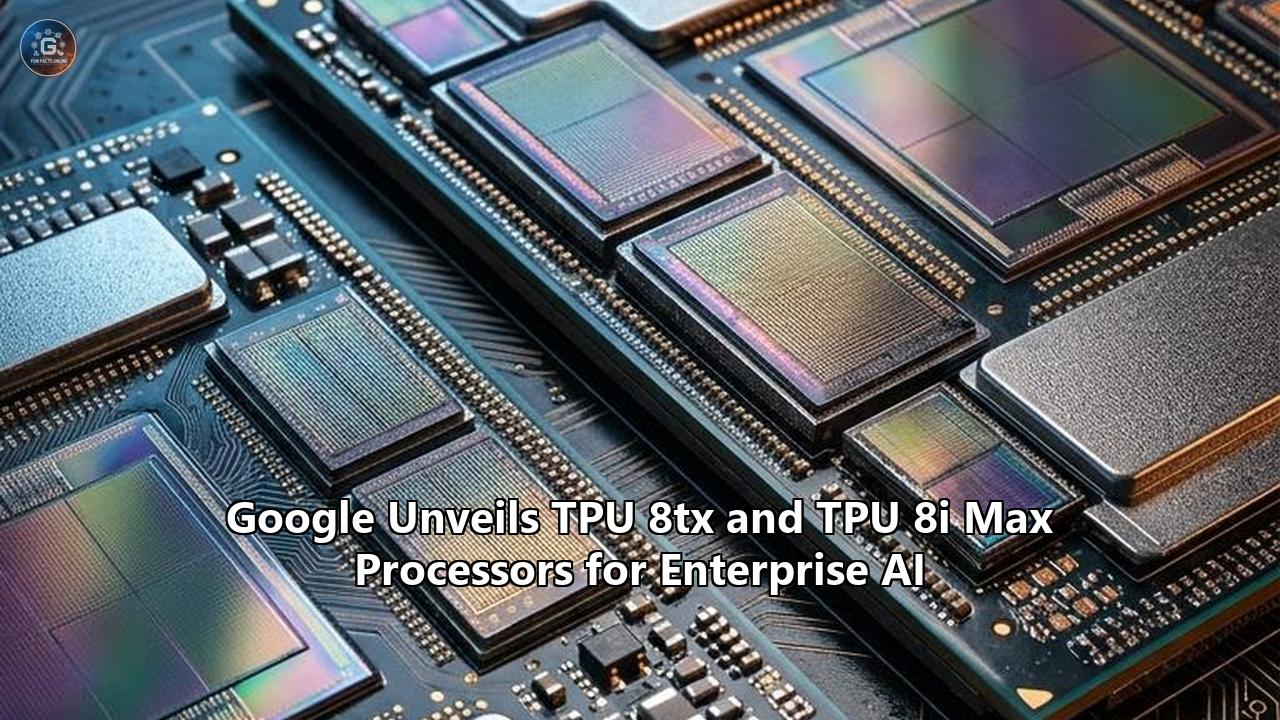
Google Cloud expanded its eighth-generation custom silicon portfolio on November 9, 2026, introducing two specialized enterprise accelerators: the TPU 8tx and the TPU 8i Max. The release marks an unprecedented acceleration in the company’s hardware cadence, bringing the total number of eighth-generation Tensor Processing Unit systems to four within a single calendar year. Rather than issuing an across-the-board architectural overhaul, Google executed a targeted system-level reconfiguration. The TPU 8tx integrates hardware-isolated trusted execution environments to secure active enterprise model weights and data, while the TPU 8i Max combines two inference dies into a unified multi-chip package to dismantle the memory bandwidth bottleneck choking long-context AI agents.
The deployment directly addresses two persistent roadblocks preventing regulated enterprises from scaling autonomous AI systems into production: memory exhaustion during long-context agent execution, and the legal inability to run proprietary or regulated data through unshielded accelerator memory. By pairing existing silicon with specialized network fabrics, fifth-generation AMD EPYC host processors, and advanced multi-chip packaging, Google is decoupling accelerator performance from the traditional multi-year silicon tape-out cycle.
Amin Vahdat, Google’s Senior Vice President and Chief Technologist for AI and Infrastructure, characterized the expansion as a fundamental shift in how cloud providers construct accelerator infrastructure. "While flexible across workloads, together the four systems in our eighth-generation TPUs give customers a purpose-built accelerator for every stage of the agentic lifecycle," Vahdat stated. The commercial stakes behind this hardware strategy are immense. Alphabet’s cloud unit reported quarterly revenues of $30.7 billion—a 103% year-over-year surge—driven heavily by custom silicon demand. Google confirmed that its TPU customer base now spans nearly 100 enterprise accounts, including Anthropic, Apple, major algorithmic trading desks, and international intelligence agencies.
Analyzing this product rollout provides a concrete lens into the structural economics of post-monolithic AI infrastructure. As raw transistor scaling slows and pretraining gives way to complex, multi-agent reasoning, the enterprise compute race is no longer won by producing the single largest piece of silicon. Instead, winning depends on system-level recomposition: repurposing proven silicon architectures to attack specific physical constraints—memory bandwidth, network topology, and hardware security boundaries.
                     GOOGLE GENERATION-8 TPU TAXONOMY

   +-------------------------------------------------------------------+
   |                         EIGHTH-GENERATION SILICON                 |
   +---------------------------------+---------------------------------+
                                     |
               +---------------------+---------------------+
               |                                           |
         [ TRAINING DIE ]                           [ INFERENCE DIE ]
               |                                           |
        +------+------+                             +------+------+
        |             |                             |             |
        v             v                             v             v
   +----------+  +----------+                  +----------+  +----------+
   |  TPU 8t  |  | TPU 8tx  |                  |  TPU 8i  |  |TPU 8i Max|
   +----------+  +----------+                  +----------+  +----------+
   | Massive  |  |Hardware  |                  |Low-lat-  |  |Dual-die  |
   | Founda-  |  |Confiden- |                  |ency real-|  |MCM, 384GB|
   | tion     |  |tial AI,  |                  |time rea- |  |HBM, 17.2 |
   | Training |  |AMD Turin |                  |soning,   |  |TB/s band-|
   | 3D Torus |  |Boardfly  |                  |Boardfly  |  |width for |
   | Fabric   |  |Network   |                  |Topology  |  |MemoryWall|
   +----------+  +----------+                  +----------+  +----------+
Architectural Deconstruction: Inside the Google TPU 8tx Processors
Enterprise adoption of public cloud AI infrastructure has long encountered a regulatory ceiling. While encryption at rest and in transit are solved disciplines across enterprise IT, data processed inside high-performance accelerators has historically existed in the clear within on-chip registers and high-bandwidth memory (HBM). For defense agencies, sovereign government entities, and financial institutions handling personal transactional telemetry, this physical vulnerability made the deployment of cloud-hosted frontier models legally untenable.
The engineering implementation of Google TPU 8tx processors resolves this vulnerability through an end-to-end trusted execution environment (TEE) spanning host CPU and accelerator silicon. Rather than manufacturing an unproven microarchitecture, Google extracted the proven compute engine of the TPU 8t training chip and re-engineered the platform interface.
The security architecture of the Google TPU 8tx processors hinges on three distinct hardware subsystems:
- Hardware-Rooted Memory Cryptography: The accelerator incorporates dedicated AES-256 hardware cryptographic engines inside the memory controllers, encrypting all data written to HBM and on-chip SRAM with dynamically rotated keys managed by Google's custom Titan security microcontrollers.
- Cryptographic Domain Coupling via AMD EPYC "Turin": Google bypassed its internal ARM-based Axion processors for the 8tx host nodes, pairing the accelerators directly with fifth-generation AMD EPYC 9005 series CPUs. This choice allows the system to bridge AMD Secure Encrypted Virtualization-Secure Nested Paging (SEV-SNP) directly into the TPU’s memory controllers over PCIe Gen5, creating an uninterrupted, attested enclave stretching from CPU host memory into the TPU core registers.
- Attestation-Bound Weight Provisioning: Model weights cannot be decrypted within the TPU execution units without a hardware cryptographic signature validating that the host operating environment, hypervisor, and software container match the customer's attested cryptographic digest.
       TPU 8tx HARDWARE CONFIDENTIAL EXECUTION ENCLAVE

+-------------------------------------------------------------+
| HOST NODE: AMD 5th Gen EPYC ("Turin")                       |
|   +-------------------------------------------------------+ |
|   | AMD SEV-SNP Secure Memory Enclave                     | |
|   | (Encrypted Model Driver, Attestation Daemon)          | |
|   +---------------------------+---------------------------+ |
+-------------------------------|-----------------------------+
                                | PCIe Gen5 with
                                | Cryptographic Attestation
+-------------------------------|-----------------------------+
| ACCELERATOR TRAY: Google TPU 8tx System                     |
|   +---------------------------v---------------------------+ |
|   | Titan Security Chip (Key Management & Hardware Attest)| |
|   +---------------------------+---------------------------+ |
|                               | Inter-die Crypto Engine     |
|   +---------------------------v---------------------------+ |
|   | TPU 8tx Compute Die (Active AES-256 Memory Decryption)| |
|   | [256x256 MXU Arrays]      [SparseCores]               | |
|   +---------------------------+---------------------------+ |
|                               | Encrypted HBM Interface     |
|   +---------------------------v---------------------------+ |
|   | High-Bandwidth Memory (Encrypted Data & Weights in Use)| |
|   +-------------------------------------------------------+ |
+-------------------------------------------------------------+
Beyond security, the TPU 8tx radically alters the system network topology. The baseline TPU 8t utilizes an inter-chip interconnect (ICI) configured in an expanded 3D torus topology designed for ultra-large training runs spanning up to 9,216 chips. In massive 3D torus fabrics, messages must traverse up to 16 network hops between diagonally distant nodes. While acceptable for asynchronous, batch-heavy distributed training runs where gradient updates dominate communication, 16 network hops introduce unviable latency penalties for synchronous, token-by-token autoregressive generation.
To correct this, Google severed the 8t silicon from the 3D torus fabric and mated it to the "Boardfly" interconnect topology pioneered on the TPU 8i. The Boardfly network is a low-diameter, high-radix direct-connect fabric that caps the worst-case network diameter to seven hops. By dropping worst-case switching transit from sixteen hops to seven, the TPU 8tx delivers up to a 50% reduction in inter-chip communication latency compared to the TPU 8t, while incurring near-zero throughput penalties from the active cryptographic engine.
This hybrid architectural posture enables an enterprise capability previously requiring disjointed infrastructure: continuous, secure adaptation. Financial institutions and healthcare consortia can deploy a single 8tx cluster to execute parameter-efficient fine-tuning (such as low-rank adaptation or LoRA), run continuous reinforcement learning with AI feedback (RLAIF), and serve production agent inference without model weights or private context datasets ever leaving the hardware-encrypted memory enclave.
Dismantling the Memory Wall: The TPU 8i Max Multi-Chip Module
While the 8tx secures the hardware boundary, the TPU 8i Max attacks the physical barrier known throughout semiconductor engineering as the memory wall.
In traditional convolutional or small-parameter transformer workloads, system performance scaled proportionally with arithmetic density—measured strictly in raw floating-point operations per second (FLOPS). Foundation models operating in the agentic era, however, display a completely different computational profile: the memory bandwidth bottleneck.
                AUTOREGRESSIVE DECODING INTENSITY

  Arithmetic Intensity (FLOPs/Byte)
    ^
    |  COMPUTE-BOUND REGION
    |  (Prefill Phase: Large Prompt Ingestion)
    |  Dense Matrix Multiplication
    |  High Operational Reuse
    |  +----------------------------------------------+
    |
    |-------------------------------------------------- Arithmetic Threshold
    |
    |  MEMORY-BOUND REGION
    |  (Generation Phase: Token-by-Token Decoding)
    |  KV Cache Loading from HBM
    |  Very Low Arithmetic Reuse
    |  +----------------------------------------------+
    +---------------------------------------------------> Sequence / Context
When an enterprise AI agent acts over an entire enterprise software repository, cross-references corporate documentation across 500,000 tokens, or parses multi-hour video streams, the model operates in two distinct phases:
- The Prefill Phase: The system ingests the prompt context in parallel. This phase features high operational arithmetic intensity (FLOPs per byte transferred) and saturates the Matrix Multiply Units (MXUs).
- The Generation (Autoregressive Decode) Phase: The model generates one token at a time. To generate a single token, the accelerator must sweep the model weights and the entire accumulated Key-Value (KV) cache out of high-bandwidth memory, push them through the compute registers, calculate the probability distribution, and append the new token.
During token generation, the arithmetic intensity plummets to fractions of a FLOP per byte. Compute cores sit idle, starved for data while waiting on the memory subsystem. As the context window expands to one million tokens and beyond, the KV cache alone expands into hundreds of gigabytes per concurrent user session.
Physical Packaging and Microarchitecture
Rather than initiating an expensive tape-out on a sub-2nm node to produce a monolithic die that would suffer from low fabrication yields and physical thermal constraints, Google engineered the TPU 8i Max as a dual-chip multi-chip module (MCM).
           TPU 8i MAX MULTI-CHIP MODULE (MCM) SCHEMATIC

+---------------------------------------------------------------+
|                      PACKAGE SUBSTRATE                        |
|                                                               |
|   +-----------------------+       +-----------------------+   |
|   |     TPU 8i DIE 0      |       |     TPU 8i DIE 1      |   |
|   |                       |       |                       |   |
|   |  +-----------------+  |       |  +-----------------+  |   |
|   |  | 384 MB On-Chip  |  |       |  | 384 MB On-Chip  |  |   |
|   |  | SRAM Register   |  |       |  | SRAM Register   |  |   |
|   |  +-----------------+  |  D2D  |  +-----------------+  |   |
|   |                       | Ultra-|                       |   |
|   |  +-----------------+  |<----->|  +-----------------+  |   |
|   |  | 256x256 Dual    |  | Wide  |  | 256x256 Dual    |  |   |
|   |  | MXU Arrays      |  | Inter-|  | MXU Arrays      |  |   |
|   |  +-----------------+  | face  |  +-----------------+  |   |
|   |                       |       |                       |   |
|   |  +-----------------+  |       |  +-----------------+  |   |
|   |  | 192 GB HBM3E    |  |       |  | 192 GB HBM3E    |  |   |
|   |  | (8.6 TB/s)      |  |       |  | (8.6 TB/s)      |  |   |
|   |  +-----------------+  |       |  +-----------------+  |   |
|   +-----------------------+       +-----------------------+   |
|                                                               |
|   Total Package Capacity:  384 GB HBM3E                       |
|   Aggregate Bandwidth:     17.2 TB/s                          |
|   Total On-Chip SRAM:      768 MB                             |
+---------------------------------------------------------------+
The system packages two complete TPU 8i dies onto an organic high-density interposer connected by an ultra-wide, low-latency die-to-die (D2D) interface. The resulting performance metrics illustrate why system-level packaging has become the dominant battleground in artificial intelligence silicon:
- High-Bandwidth Memory (HBM3E): Reaches 384 GB per package—a 33% increase over single-die high-end configurations and double the baseline TPU 8i capacity.
- Aggregate Memory Bandwidth: Scales linearly to 17.2 TB/s across the package, providing the throughput needed to sweep large KV caches without stalling execution units.
- On-Chip High-Speed SRAM: Expands to 768 MB per multi-chip package, allowing entire attention layers and persistent speculative decoding draft matrices to remain entirely on-die.
- Compute Density: Delivers exactly double the peak theoretical FP8/BF16 matrix math capacity of the standard 8i within an identical physical slot layout.
Data Center Rack Density and Thermal Efficiency
The primary commercial impact of the TPU 8i Max packaging strategy emerges at the data center rack level. Cloud facilities face severe power delivery and floor-space constraints; modern megawatt deployments cannot simply expand footprint indefinitely. Because the 8i Max places two logical accelerators into the physical rack space and thermal distribution previously allocated to a single accelerator tray, Google has doubled compute and memory capacity per square meter.
By integrating cold-plate liquid cooling blocks directly across the shared heat spreader of the MCM package, Google manages thermal dissipation without expanding rack dimensions. This allows data center engineers to deploy massive model concurrency within enterprise facilities where building new structural shells or expanding electrical substation intake is commercially or physically impossible.
Architectural Comparison: Eighth-Generation TPU Systems
The following technical breakdown details how Google has divided its eighth-generation silicon portfolio to target distinct operational vectors across the artificial intelligence engineering stack:
| Architectural Metric | TPU 8t (Scale-Up Training) | TPU 8i (Reasoning Engine) | TPU 8tx (Confidential / Hybrid) | TPU 8i Max (High-Context MCM) |
|---|---|---|---|---|
| Primary Workload | Frontier Pretraining, Exascale Foundation Models | Real-time Low Latency Inference | Hardware-Isolated Fine-Tuning & Secure Inference | Long-Context Agentic Workflows, Video Analytics |
| Silicon Package Form | Monolithic Training ASIC | Monolithic Inference ASIC | Monolithic Training ASIC + Hardware Crypto Engine | Dual-Die Multi-Chip Module (MCM) |
| Host CPU Architecture | Google Custom Axion (ARM-based) | Google Custom Axion (ARM-based) | AMD 5th Gen EPYC ("Turin") via SEV-SNP | Google Custom Axion (ARM-based) |
| Interconnect Topology | 3D Torus Fabric (High Diameter, Max 16 Hops) | Boardfly Direct-Connect (Low Diameter, Max 7 Hops) | Boardfly Direct-Connect (Low Diameter, Max 7 Hops) | Boardfly Direct-Connect + Dual-Die Coherent D2D |
| HBM Subsystem Capacity | Up to 192 GB HBM3E | 288 GB HBM3E | Up to 192 GB Encrypted HBM3E | 384 GB Unified HBM3E |
| Memory Bandwidth | 8.6 TB/s | 8.6 TB/s | 8.6 TB/s (Hardware Encrypted) | 17.2 TB/s |
| On-Chip SRAM | 384 MB | 384 MB | 384 MB | 768 MB |
| Security Enforcement | Data at rest/transit encryption | Data at rest/transit encryption | Hardware-Enforced Active Memory Confidential Enclave | Data at rest/transit encryption |
Strategic Analysis: The Enterprise Custom Silicon Playbook
The launch of the TPU 8tx and TPU 8i Max offers an empirical case study of how custom silicon development has evolved inside hyperscale cloud providers. Examining the mechanics of this rollout highlights three clear industry principles:
               THE SYSTEM RECOMPOSITION ADVANTAGE

   TRADITIONAL SILICON CADENCE:
   [ Tape-Out Gen 1 ] --------(24-36 Months)--------> [ Tape-Out Gen 2 ]
   * Massive $100M+ NRE CapEx
   * Long iteration cycle
   * High failure/delay risk

   SYSTEM RECOMPOSITION CADENCE:
   [ Core Tape-Out ]
          |
          +--(Month 0)--> System A: Base Training (TPU 8t)
          |
          +--(Month 6)--> System B: Re-interconnect + Crypto (TPU 8tx)
          |
          +--(Month 6)--> System C: MCM Multi-Die Stitching (TPU 8i Max)
   * Amortized mask/die costs
   * Sub-12 month delivery to market
   * Direct alignment to emergent software workloads
Principle 1: System Recomposition Beats Silicon Reinvention
During the first decade of hardware acceleration, competitive advantage was defined by monolithic improvements: shrinking the process node from 16nm to 7nm, then to 5nm and 3nm, while enlarging the physical die toward the reticle limit.
That paradigm has broken down under physical and fiscal realities. Leading-edge silicon tape-outs on nodes below 3nm regularly surpass $100 million in non-recurring engineering (NRE) expenses, while physical reticle limits restrict how large a single die can be cast without yields plummeting.
Google’s eighth-generation portfolio illustrates the counter-strategy: Platform Recomposition.
Instead of designing four separate processors, Google designed two fundamental silicon building blocks—the training die and the inference die. By altering the supporting substrate, the interconnect layer, the host processor pairing, and the packaging strategy, Google created four distinct commercial systems targeting completely different enterprise budgets and operational profiles within months:
- The training die operates over a 3D torus for exascale cluster synchronization (TPU 8t) or drops into a Boardfly network with cryptographic controllers for confidential enterprise workloads (TPU 8tx).
- The inference die runs independently for cost-sensitive standard reasoning (TPU 8i) or mounts side-by-side on an organic MCM substrate to shatter the memory wall for long-context agents (TPU 8i Max).
Through this approach, Google amortizes base silicon development costs over vastly higher production volumes while cutting time-to-market for specialized systems from years to months.
Principle 2: Hardware-Enforced Security Is Table Stakes for Enterprise Autonomy
Enterprise artificial intelligence is pivoting away from conversational chatbots toward autonomous agents—software entities authorized to read corporate databases, issue API calls, synthesize proprietary operational logs, and execute financial transactions.
This functional transition changes the underlying risk model. While public-facing chat applications tolerate shared cloud memory constructs, autonomous enterprise agents cannot. Corporate security officers, compliance committees, and institutional risk officers routinely block AI deployments because of the "cleartext in memory" problem. Standard cloud virtualization does not defend against a compromised hypervisor, a rogue cloud administrator, or memory-dump attacks via hardware side-channels.
The enterprise adoption pattern evident in the deployment of Google TPU 8tx processors proves that confidential computing is no longer a peripheral compliance checkmark. Hardware-rooted isolation is now the foundational gating requirement for the enterprise AI economy.
By providing cryptographically verifiable proof of what code and weights are executing in the accelerator, Google TPU 8tx processors transform cloud infrastructure into a zero-trust enclave. For regulated verticals like algorithmic trading, biomedical discovery, and cross-border banking, this capability unlocks private fine-tuning and active deployment without exposing competitive intellectual property to cloud host operators or co-tenant side-channel exploits.
Principle 3: Compute and Memory Scaling Have Decoupled
For over twenty years, computer architects operated under the assumption that arithmetic capability and memory bandwidth could advance along parallel paths. The explosion of autoregressive sequence processing severed this assumption.
The TPU 8i Max provides explicit empirical proof that for reasoning and agentic workflows, compute capacity is no longer the scarce resource. The binding constraint is memory residency and memory channel capacity.
When software architectures shift toward agentic decomposition—where five to twenty independent specialized agents loop repeatedly over an entire multi-million token code repository—the entire execution graph becomes memory-bound. Accelerators that focus exclusively on maximizing FLOPS sit idle, throttled by narrow memory buses. By designing a system that doubles the memory bus to 17.2 TB/s and on-chip SRAM to 768 MB, Google is targeting performance gains where modern models actually execute: at the memory interface.
Market Realignment: Hyperscalers, Merchant Silicon, and the Ecosystem
The arrival of the TPU 8tx and TPU 8i Max alters the broader commercial balance of power among merchant silicon vendors, cloud providers, and enterprise buyers.
                THE HYPERSCALER HARDWARE REALIGNMENT

   +-------------------------------------------------------------+
   |                      MERCHANT VENDORS                       |
   |                                                             |
   |   NVIDIA (Blackwell / Rubin)       AMD (Instinct MI350/400) |
   |   - Universal Enterprise Standard  - Open-Source ROCm Focus |
   |   - CUDA Software Monopoly         - Aggressive Value Eng.  |
   +------------------------------+------------------------------+
                                  |
                   MARKET PRESSURE AND CO-OPETITION
                                  |
   +------------------------------v------------------------------+
   |                 CUSTOM HYPERSCALER SILICON                  |
   |                                                             |
   |   GOOGLE CLOUD: Generation-8 TPU Ecosystem                  |
   |   - TPU 8t (Training)     - TPU 8i (Reasoning)              |
   |   - TPU 8tx (Confidential)- TPU 8i Max (Memory Wall MCM)    |
   |                                                             |
   |   KEY ENABLERS:                                             |
   |   * TorchTPU / OpenXLA: Dismantling CUDA Exclusivity        |
   |   * AMD Turin Sockets: Strategic Hyperscaler Cross-Pollinate|
   |   * Direct TCO Advantage: Zero Merchant Margin Markups     |
   +-------------------------------------------------------------+
The Shifting Dynamics Between Google, NVIDIA, and AMD
Historically, the public cloud ecosystem operated along clear lines: cloud providers built data centers, purchased generic server CPUs from Intel or AMD, and acquired accelerated computing gear directly from NVIDIA.
Google’s expansion to four discrete eighth-generation TPU systems highlights how aggressively hyperscalers are rewriting this relationship. While Google continues to purchase high volumes of NVIDIA’s Blackwell and upcoming Rubin platforms to serve customers committed to the CUDA ecosystem, the TPU portfolio serves an entirely different financial and strategic function: margin insulation and cloud differentiation.
Every enterprise customer migrating from a merchant GPU instance to a TPU cluster directly expands Google Cloud’s operating margins by eliminating the hefty gross margin markups collected by merchant silicon providers.
The inclusion of AMD in the TPU 8tx design represents a sophisticated commercial dynamic. While AMD competes directly with Google in AI acceleration via its Instinct MI350 and MI400 series GPUs, Google turned directly to AMD’s fifth-generation EPYC "Turin" server processors to power the TPU 8tx host infrastructure. AMD secured an indispensable socket in Google's enterprise acceleration architecture because of its mature, hardware-attested SEV-SNP confidential computing ecosystem. This reflects a pragmatic strategy: rather than waiting for its proprietary ARM-based Axion platform to clear lengthy enterprise security audits, Google integrated AMD’s proven host security foundation to immediately open regulated markets.
Eradicating the CUDA Software Moat
Silicon is only as capable as the software framework that compiles code down to its execution units. For more than a decade, NVIDIA maintained an effective monopoly over accelerated computing through CUDA—its deeply entrenched proprietary software framework.
Google’s commercial TPU push is succeeding where previous initiatives stumbled because the software center of gravity has shifted away from hardware-specific toolchains toward framework-level abstraction:
- TorchTPU: Google, in direct engineering collaboration with Meta, launched TorchTPU as a production open-source project. Engineers can execute native PyTorch code directly on TPU clusters without code rewrites, kernel refactoring, or reliance on complex manual translation layers.
- vLLM Integration: The industry-standard open-source vLLM serving engine now natively incorporates a downstream TPU backend. Enterprise developers deploy quantized models, continuous batching, and PagedAttention primitives onto TPUs via standard containerized APIs identical to GPU serving stacks.
- OpenXLA Ecosystem: The OpenXLA consortium—backed by Google, Apple, Amazon Web Services, Meta, and AMD—has established a unified open-source compiler infrastructure. Graph optimizations and kernel lowerings occur automatically, transforming custom silicon into a fungible, compiler-managed utility rather than an esoteric hardware niche.
By standardizing on PyTorch and vLLM compatibility, Google has eliminated the software switching costs that historically locked enterprise developers into CUDA-dependent infrastructure.
Practical Deployment Architecture: Sizing Enterprise Workloads
For enterprise infrastructure architects, systems directors, and engineering leads, the arrival of four distinct systems within a single generation requires a rigorous selection methodology. The decision matrix below presents concrete guidelines for matching enterprise AI workloads to optimal hardware targets:
               ENTERPRISE HARDWARE SELECTION TOPOLOGY

                       [ Workload Initiation ]
                                  |
              Is the workload subject to strict regulatory,
              sovereign, or memory-cleartext compliance?
                                  |
                 +----------------+----------------+
                 | YES                             | NO
                 v                                 v
        [ Deploy TPU 8tx ]                 What is the operational
        * AMD SEV-SNP Enclave              computational focus?
        * Active Memory Encryption                 |
        * Secure Fine-Tuning & Serving             |
                 +---------------------------------+
                 |                                 |
                 v                                 v
        [ Large-Scale Training ]         [ Production Inference ]
                 |                                 |
        Does training exceed              Does the inference model
        100B params from scratch?         require massive contexts /
                 |                        multi-turn agent KV caches?
        +--------+--------+                        |
        | YES             | NO            +--------+--------+
        v                 v               | YES             | NO
   [ TPU 8t ]       [ TPU 8tx ]           v                 v
   * 3D Torus       * Boardfly Fabric [TPU 8i Max]      [ TPU 8i ]
   * Exascale Pods  * Low Latency     * Dual-Die MCM    * Standalone
                                      * 17.2 TB/s HBM   * Ultra-Low
                                      * 384 GB Unified    Latency
1. Regulated Enterprise Fine-Tuning & Multi-Agent Inference: TPU 8tx
Enterprise teams working within healthcare, banking, defense, or critical infrastructure should target Google TPU 8tx processors when the following requirements dominate:
- Sovereignty & Isolation: Legal mandates strictly prohibit running data across unencrypted memory infrastructure.
- Integrated Adaptation Cycles: The pipeline alternates between real-time token generation and ongoing local model tuning (e.g., continuous Reinforcement Learning from Human Feedback or private LoRA adaptation).
- Low-Latency Communication: Distributed inference requires rapid token iteration across small-to-medium cluster configurations, where the 7-hop Boardfly network prevents communications thrashing.
2. Deep Context Parsing & Agent Swarms: TPU 8i Max
Engineering teams building agentic software pipelines that operate across deep token windows should default to the TPU 8i Max:
- Massive Active KV Caches: Serving large models (70B+ parameters) with context windows exceeding 500,000 tokens per stream, where token-by-token generation is blocked by memory bus throughput.
- Multi-Modal Video & Code Processing: Ingesting hours of multi-modal surveillance feeds, real-time audio streams, or enterprise-wide software repositories where multiple gigabytes of context must remain persistently active across decoding steps.
- Density-Constrained Private Colocation: Maximizing rack compute output within data centers facing power draw limits, replacing two discrete inference accelerator trays with a unified MCM package.
3. Exascale Foundation Pretraining: TPU 8t
Teams training frontier foundation architectures from raw weights should continue deploying the baseline TPU 8t:
- Cluster Scaling Beyond 1,000 Nodes: Workloads benefit from the 3D torus interconnect topology, scaling to 9,216 chips where massive bisection bandwidth outranks hop-by-hop message delivery latency.
- High Operational Arithmetic Reuse: Massive batch sizes maximize FLOPS utilization inside the 256x256 systolic arrays, keeping execution units saturated without suffering from the memory wall that impacts single-token generation.
The Road Ahead: System-Level Challenges and What to Watch
While the introduction of the TPU 8tx and TPU 8i Max resolves critical security and memory bottlenecks, it introduces several complex engineering trade-offs that IT leaders must monitor through 2027 and beyond.
The primary engineering challenge centers on thermal dissipation and liquid cooling logistics. Packaging two high-performance dies side-by-side inside the TPU 8i Max creates intense thermal heat flux densities across the MCM package. Standard forced-air cooling racks cannot service these density profiles.
Enterprise facilities adopting these systems must accelerate their migration toward direct-to-chip liquid cooling loops and liquid-to-air secondary heat exchangers. Organizations lacking updated raised-floor mechanical cooling, automated coolant distribution units (CDUs), and leak-detection safety infrastructure will find themselves physically incapable of mounting high-density dual-chip trays.
A second operational variable involves the long-term software support matrix for heterogeneous CPU-TPU pairing. The integration of AMD EPYC "Turin" CPUs inside the TPU 8tx demonstrates engineering agility, but it diverges from Google’s broader internal roadmap centered on its ARM-based Axion processors.
Infrastructure teams must watch whether Google eventually extends hardware-level confidential attestation directly to Axion-hosted nodes, or whether the company maintains a dual-architecture host strategy indefinitely. Sustaining two distinct hypervisor kernel drivers, attestation engines, and system firmware trees across enterprise deployments inevitably increases software maintenance overhead and validation complexity.
Finally, the competitive response from the broader merchant market will reshape pricing across hyperscale computing. NVIDIA’s Blackwell Ultra (B300) and upcoming Rubin platforms, alongside AMD’s Instinct MI350/MI400 series, are accelerating their own moves toward high-capacity HBM4 integration and advanced chiplet packaging.
As hyperscale cloud providers increasingly demonstrate that recomposed custom silicon can run enterprise workloads at lower operational costs, the pricing power of merchant hardware will face sustained pressure. The unveiling of Google's specialized eighth-generation processors proves that the competitive center of AI infrastructure has permanently shifted: success is no longer dictated by single-die transistor counts, but by the strategic engineering of the complete system around the workload.
Reference:
- https://shiftdelete.net/en/google-tpu-8tx
- https://thenextweb.com/news/google-reportedly-adds-two-tpu-variants
- https://www.constellationr.com/insights/news/google-launches-tpu-8tx-tpu-8i-max
- https://www.servethehome.com/google-tpu-8tx-8i-max-amd-epyc-turin/
- https://www.techpowerup.com/354620/google-extends-tensor-processor-unit-series-with-tpu-8tx-and-8i-max
- https://www.forbes.com/sites/jonmarkman/2026/11/10/google-adds-tpu-8tx-and-8i-max-as-its-ai-chip-business-nears-100-customers/
- https://www.igorslab.de/en/google-expands-tpu-generation-8tx-amd-epyc-confidential-ai-8i-max-double-memory-bandwidth/
- https://newsletter.semianalysis.com/p/tpuv7-google-takes-a-swing-at-the
- https://introl.com/blog/google-tpu-architecture-complete-guide-7-generations
- https://medium.com/womenintechnology/google-cloud-tpu-architecture-versions-explained-from-v1-to-the-eighth-generation-3f2371962154
- https://gist.github.com/philschmid/68c5afacfd3a3555ca834ba27415ba88
- https://docs.cloud.google.com/tpu/docs/v6e