
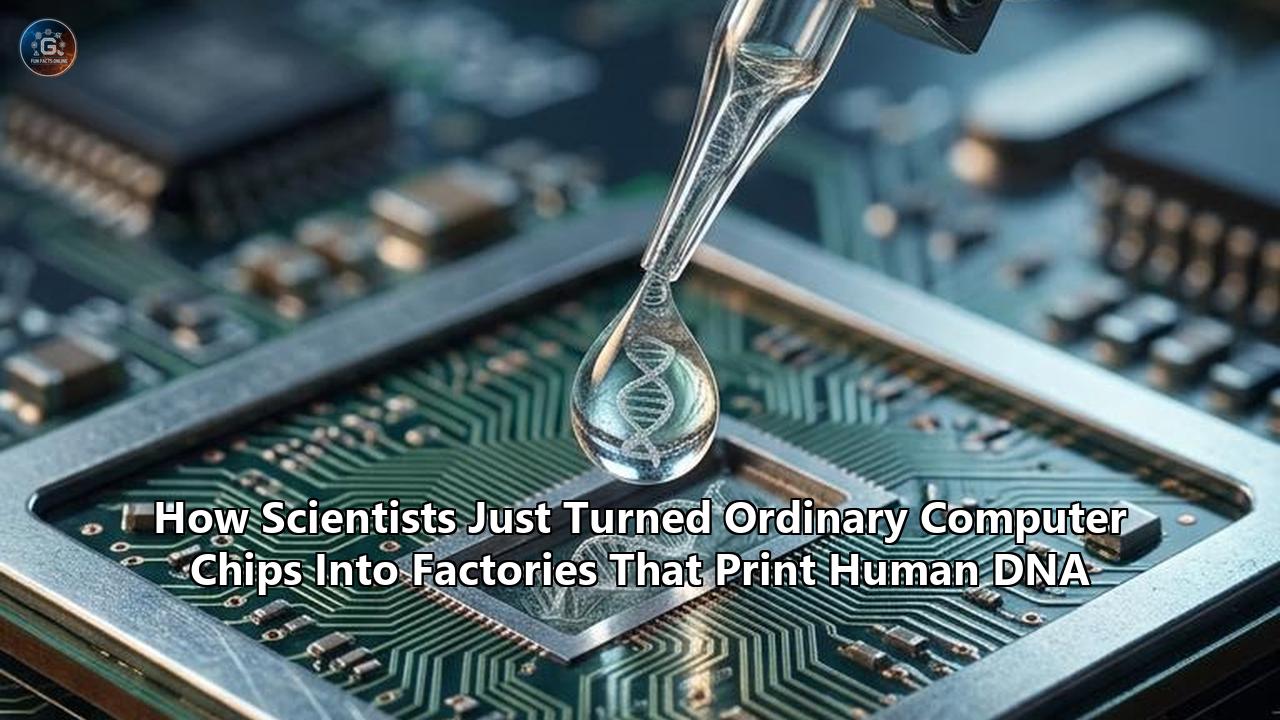
On June 17, 2026, a research team led by Harvard University’s John A. Paulson School of Engineering and Applied Sciences (SEAS) published a paper in Nature Electronics that bridged the historic gap between microelectronics and molecular biology. The researchers demonstrated that a standard silicon computer chip—the very hardware that powers smartphones, servers, and neural network accelerators—could be transformed into a highly precise, water-based factory capable of printing human DNA.
By successfully synthesizing 64 distinct genetic sequences simultaneously on a single semiconductor surface, the team, led by Donhee Ham, established a new benchmark for parallel enzymatic synthesis in water.
This development represents a fundamental shift in how the physical world of computing interfaces with organic chemistry. Historically, manufacturing custom DNA has been an expensive, highly centralized, and environmentally hazardous endeavor. It has required dedicated industrial facilities utilizing toxic, solvent-heavy chemical processes.
The Harvard-led breakthrough bypasses these limitations by orchestrating enzymatic synthesis via micro-electrodes, utilizing water as the primary reaction medium and electric currents as the primary control mechanism.
To demonstrate the precision and viability of this silicon-biology interface, the researchers encoded a 169-byte digital text message directly into the synthesized DNA strands.
This achievement does not merely introduce a faster method for biological synthesis; it serves as a powerful case study in how mature, scaled industrial hardware can be adapted to solve the bottlenecks of biological manufacturing. Analyzing this development reveals key principles of substrate repurposing, software-defined chemistry, and the emerging realities of decentralized biotechnology.
Repurposing the Neural Eavesdropper
To understand how the team printed DNA on a computer chip, it is first necessary to examine the physical hardware they used. The silicon chip at the heart of this experiment was not designed for genetic engineering. It was originally built by Jeffrey Abbott, a former PhD student in Donhee Ham’s lab, to listen to the brain.
   Original CMOS Design:                   Repurposed DNA Synthesis Design:
+--------------------------+             +-------------------------------------+
|                          |             |       Active Proton Scavenging      |
|  [ Neuronal Membrane ]   |             |   [Outer Electrode] Reclaims Protons|
|            |             |             |          \       /                  |
|            v             |    ---->    |     +-----\-----/-----+             |
|  [Micro-hole Electrode]  |             |     |   [Inner Ring]  |             |
|  Pore-permeabilizing     |             |     |   Generates H+  |             |
|  intracellular sensor    |             |     |   (lowers pH)   |             |
|                          |             |     +--------v--------+             |
+--------------------------+             +-------------------------------------+
                                               (Triggers local deprotection)
The chip was a high-density complementary metal-oxide-semiconductor (CMOS) microelectrode array engineered for population-scale, intracellular neuronal recording. Its primary purpose was to measure the faint, millivolt-scale electrical fluctuations of thousands of firing brain cells simultaneously. To achieve intracellular access, the chip used precise, localized current injection to temporarily permeabilize the lipid bilayers of neuronal membranes without destroying the cells.
The researchers realized that the same micro-level precision required to inject current into living neurons could be reversed and redirected to control localized chemical reactions.
By altering the surface chemistry of the array and modifying the electrode designs, the team converted the passive, signal-reading device into an active, molecular-writing engine.
"At a certain point, we wondered whether that same current control could be redirected from cells to molecules—replacing the neuron-facing electrodes with ring-electrode pairs that could localize pH for DNA synthesis," Ham explained. "It worked."
This transition highlights an elegant engineering lesson: the physics of electrical charge transport do not change when moving from neurological tissues to biochemical solutions.
A high-density electrode array is, at its core, a spatial mapping engine. Whether it maps the voltage potentials of a neural network or orchestrates the electrochemical states of liquid droplets, the underlying electronic architecture remains the same. By hacking this existing substrate, the researchers avoided the decade-long, multi-million-dollar cycle of designing, fabricating, and debugging an entirely new class of microfluidic or microelectronic hardware from scratch.
Controlling Diffusion Without Physical Walls
The primary technical hurdle in water-based, parallel DNA synthesis is the natural law of diffusion. In a liquid medium, molecules do not stay in one place. When an electric current is used to alter the chemical environment at one micro-scale coordinate, those changes rapidly spread outward, contaminating adjacent reaction zones.
To synthesize distinct DNA strands side-by-side, each of the chip's 64 synthesis sites must behave as an isolated, virtual reaction vessel. If the chemical triggers from one site drift into another, the sequences become scrambled, rendering the output useless.
The Harvard team, working in collaboration with the Broad Institute, POSTECH, and the French biotechnology firm DNA Script, resolved this spatial contamination problem through a dual-concentric ring electrode architecture.
                  +----------------------------------+
                  |     Liquid Water & Enzymes       |
                  +----------------------------------+
                             /            \
                            v              v
               +----------------------------------------+
               |  Outer Ring Electrode (Proton Sink)    |
               |  - Pulls current                       |
               |  - Consumes escaping H+ ions           |
               |  - Prevents cross-site contamination   |
               +----------------------------------------+
                                    |
                                    v
               +----------------------------------------+
               |  Inner Ring Electrode (Proton Source)  |
               |  - Drives localized current            |
               |  - Splits water to generate H+ ions    |
               |  - Lowers pH locally to trigger reaction|
               +----------------------------------------+
                                    |
                                    v
                        [Anchored DNA Molecules]
At each of the 64 programmable sites, the growing DNA strands are anchored at the center, surrounded by two concentric micro-scale gold rings. The synthesis relies on enzymatic reactions that are highly sensitive to pH. To attach a new nucleotide (A, C, T, or G) to the growing chain, the temporary blocking group at the end of the strand must first be removed. This process—known as deprotection—only occurs under acidic conditions (low pH).
The concentric ring design coordinates this deprotection cycle with spatial control:
- Local Acidification (The Inner Ring): To trigger deprotection at a chosen site, the chip sends a precise electric current through the inner ring electrode. This current splits water molecules in a localized electrolysis reaction, generating a high concentration of protons ($H^+$ ions). This lowers the pH to an acidic level directly above the anchored DNA strands, removing the blocking group and preparing the strand for the next nucleotide.
- Electrochemical Containment (The Outer Ring): Left unchecked, these protons would immediately diffuse outward through the water, lowering the pH at neighboring sites and causing unintended deprotection. To prevent this, the chip simultaneously pulls current from the outer ring electrode. This outer ring acts as an electrochemical scavenger, consuming the migrating protons as they drift away from the center.
By establishing this active, electronic boundary, the researchers restricted the acidic zone to a tiny, microscopic droplet directly above the target sequence. This allowed the chip to write 64 completely distinct DNA sequences simultaneously, in parallel, without requiring physical walls, microchannels, or mechanical valves to separate the reactions.
Disruption of the Phosphoramidite Paradigm
To appreciate why this microelectronic approach is a milestone, it must be evaluated against the historic standards of genetic synthesis. For over forty years, the biotechnology industry has relied almost exclusively on phosphoramidite chemistry to write DNA.
While phosphoramidite chemistry is highly mature and capable of producing millions of custom sequences in massive, centralized industrial facilities, it is fundamentally incompatible with the demands of decentralized modern medicine and emerging data-storage frameworks.
| Feature | Legacy Phosphoramidite Chemistry | Chip-Based Enzymatic DNA Printing |
|---|---|---|
| Reaction Medium | Hazardous, toxic organic solvents (e.g., acetonitrile) | Mild, biocompatible liquid water |
| Infrastructure | Centralized, high-throughput industrial factories | Decentralized, portable silicon microchips |
| Environmental Impact | High chemical waste; intensive disposal requirements | Low waste; clean, water-based enzymatic byproducts |
| Reaction Trigger | Complex, multi-step liquid reagent exchanges | Locally controlled electrical currents and pH tuning |
| Parallelization Method | Physical microfluidics, physical wells, or inkjet arrays | Software-defined concentric electrode containment |
| Safety Profile | Requires chemical hoods and specialized storage | Highly safe; suitable for standard labs and clinics |
Phosphoramidite chemistry requires a series of organic solvents, including acetonitrile, to wash, couple, cap, and oxidize each nucleotide added to a sequence. These solvents are highly toxic, flammable, and pose significant environmental disposal challenges. Because of the hazards associated with handling these chemicals, custom DNA synthesis has remained largely centralized.
When a researcher, hospital, or defense laboratory needs a custom gene or diagnostic probe, they must order it from a centralized provider (such as Twist Bioscience or Integrated DNA Technologies) and wait days or weeks for the physical sample to be synthesized, purified, packaged, and shipped.
Enzymatic DNA synthesis, by contrast, operates in water under mild conditions, mimicking how living cells write their own genetic material. This eliminates toxic organic solvents, enabling a much safer, environmentally friendly manufacturing profile.
However, prior to the Harvard team's work, enzymatic methods struggled with scalability, generally limited to writing a dozen or fewer sequences in parallel.
By successfully demonstrating that a silicon chip can coordinate 64 parallel enzymatic reactions using localized electric currents, the research group proved that DNA printing technology can scale without the need for toxic chemistry. This brings the field closer to realizing small, portable, and accessible DNA-writing instruments—effectively "desktop gene printers" that can sit on the workbench of any laboratory, clinic, or remote military outpost.
Architectural Lessons from the Silicon-Biology Interface
The success of the Harvard SEAS experiment offers several design and architectural lessons for engineering hybrid biological-silicon systems. These lessons extend far beyond genetic synthesis, offering a blueprint for how future deep-tech innovations can navigate the physical limitations of both biology and electronics.
Principle 1: Substrate Versatility and 'Hardware Hacking' in Deep Tech
The conventional approach to developing a new biotechnology platform is to design bespoke hardware optimized for a specific chemical reaction. While this approach yields high theoretical performance, it ignores the immense economic and practical advantages of existing manufacturing lines.
The semiconductor industry has spent over half a century and trillions of dollars optimizing the fabrication of silicon CMOS wafers. Designing custom silicon chips is incredibly expensive, with tape-out costs for modern fabrication runs easily running into hundreds of thousands or millions of dollars.
                                [ Mature Semiconductor Ecosystem ]
                                  (Trillions in R&D, Scaled Fab Lines)
                                                |
                                                v
    +-------------------------------------------+-------------------------------------------+
    |                                                                                       |
    v                                                                                       v
[ Conventional Biotech Route ]                                              [ Substrate Repurposing Route ]
- Design custom, bespoke hardware                                           - Identify existing silicon architecture (e.g., CMOS, RF)
- High tape-out costs ($100k-$1M+)                                          - Modify surface-level electrode geometries
- Slow, iterative design loops (years)                                      - Maintain underlying power & control systems
- Custom manufacturing scale-up hurdles                                     - Instantly inherit mature, low-cost scaling
By identifying that a mature, existing neural-recording CMOS chip possessed the identical sub-microampere current injection capabilities required for water electrolysis, Donhee Ham’s team bypassed these massive barriers. They preserved the underlying electronic architecture of the chip—the complex row/column address decoders, the current mirrors, and the power delivery networks—and merely modified the surface-level electrode geometries.
This lesson is highly applicable to other fields: when building physical-digital interfaces, innovators should seek to "hack" mature, scaled silicon substrates (such as RF chips, camera sensors, or memory arrays) rather than inventing new fabrication protocols.
Principle 2: Software-Defined Spatial Chemistry
Traditional microfluidics relies on physical structures—microscopic channels, chambers, elastomeric valves, and pumps—to route chemicals to specific physical locations. While effective at macroscopic scales, physical microfluidics becomes notoriously unreliable as it scales down.
Valves clog, channels leak, surface-tension issues dominate, and the mechanical complexity of routing thousands of discrete fluid streams becomes a design bottleneck.
The concentric ring electrode solution replaces physical structures with electromagnetic fields. The "walls" of each reaction chamber on the Harvard chip are entirely virtual; they exist only because of the balance of electrical currents flowing through the inner and outer rings. If the researchers want to change the size, shape, or intensity of a reaction zone, they do not need to rebuild the hardware. They simply change a line of code in the software controlling the current output.
This software-defined chemistry vastly simplifies physical manufacturing. Instead of complex, multi-layered polymer chips bonded to silicon, the device remains a flat, easily cleanable silicon surface.
Future scaling to thousands or millions of parallel reactions will not require increasingly complex plumbing; it will require higher-density electronic routing, a challenge that the semiconductor industry has already solved through Moore’s Law.
       Physical Microfluidic Routing:                    Software-Defined Electro-Chemical Routing:
   +------------------------------------+             +----------------------------------------------+
   |   [Physical Valve]  [Clogging risk]|             |                                              |
   |          |                |        |             |  [H+ zone] <--- Virtual electrostatic walls  |
   |          v                v        |   VS.       |   (Controlled entirely via software-defined  |
   |   [Microfluidic Channels] [Leaks]  |             |    current profiles; zero moving parts)      |
   |                                    |             |                                              |
   +------------------------------------+             +----------------------------------------------+
Principle 3: The Translation Bottleneck—When Silicon Outpaces Biology
A defining insight from this case study is the direct identification of the primary bottleneck in the system. When analyzing the performance limits of the platform, the researchers discovered that the speed and density limitations were not imposed by the microelectronics.
"The chip did what we asked it to do: it localized low pH at selected sites," noted co-first author Han Sae Jung. "The limitation came from the deprotection chemistry, not from the silicon. That leaves a clear next step for the field—develop a more direct acid-driven deprotection chemistry that can keep pace with the chip."
This points to a broader challenge in bio-computational convergence. Silicon transistors switch at gigahertz speeds (billions of cycles per second). Biological processes—such as enzyme-substrate binding, nucleotide addition, and chemical deprotection—operate on millisecond-to-second scales.
Furthermore, because chemical reactions depend on the physical movement of matter rather than the flow of electrons, biological operations are fundamentally constrained by diffusion rates, molecular steric hindrance, and thermodynamic barriers.
When designing hybrid systems, engineers must prepare for this translation mismatch. The goal should not be to make the silicon run faster, but rather to exploit the massive speed margin of silicon to perform highly parallelized control loops, real-time error correction, and multi-site coordination.
The silicon chip is ready to coordinate millions of reactions at microsecond resolution; the next generation of materials scientists and molecular biologists must now develop "faster" chemistry, such as synthetic enzymes or highly responsive photo-acid generators, that can match the control speeds of modern integrated circuits.
DNA as the Next Digital Storage Medium
While the immediate benefits of this DNA printing technology are concentrated in synthetic biology and medicine, the Harvard team also used this platform to address a looming crisis in the digital world: the data storage bottleneck.
By encoding a 169-byte text message into the synthesized DNA sequences, the researchers demonstrated the real-world viability of using biology as a high-density, long-term archiving medium.
                              [ The Digital Data Deluge ]
                             (Exabytes of unstructured data)
                                            |
                                            v
    +---------------------------------------+---------------------------------------+
    |                                                                               |
    v                                                                               v
[ Silicon & Magnetic Limits ]                                       [ Biomolecular DNA Storage ]
- Magnetic tapes degrade in 10-30 years                             - Stable for thousands of years at room temp
- Flash memory has finite read/write cycles                         - Extreme spatial density (~215 petabytes per gram)
- Massive physical footprint & power grid demand                   - Maintenance-free; no power required for archiving
The global volume of digital data is expanding exponentially, driven by artificial intelligence, high-definition video, and ubiquitous sensor networks. Traditional magnetic tapes, hard drives, and flash memory systems are struggling to keep pace. These physical media degrade within 10 to 30 years, requiring continuous, energy-intensive migration of data to new hardware. Furthermore, the physical footprint and power grid demands of massive server farms are increasingly unsustainable.
Nature solved this archiving problem billions of years ago. DNA is incredibly stable; genetic material retrieved from ancient fossils can be accurately read after hundreds of thousands of years in sub-optimal conditions.
More importantly, DNA offers unmatched storage density. Theoretically, all of humanity’s digital data could be written into a few kilograms of DNA.
Using synthetic DNA as an archive has historically been blocked by the lack of write speeds and the high costs of traditional chemical synthesis. It is highly inefficient to use centralized, toxic phosphoramidite chemistry to archive exabytes of data.
By showing that a silicon chip can write distinct DNA sequences in parallel using clean, water-based chemistry, this research charts a viable path toward commercial DNA data storage.
The 169-byte demo represents a small scale, but because the writing engine is silicon-based, it can scale using the same fabrication lines that stamp out computer parts.
If a future CMOS chip can be built with millions of active, software-controlled concentric electrode sites, write speeds could increase by orders of magnitude, making molecular archiving economically viable for cold-storage data centers.
Future Frontiers: From Clinics to Biosecurity
The maturation of on-chip DNA printing technology will have profound implications for biological research, healthcare, and national security. By decentralizing the manufacturing of genetic materials, this technology shifts the balance of power from massive industrial chemical hubs to local, software-driven environments.
Personalized On-Demand Therapeutics
The current paradigm of medicine relies on large-scale pharmaceutical manufacturing and complex cold-chain logistics to deliver therapies to patients. In the future, desktop gene printers powered by silicon chips could allow hospitals to print personalized cancer therapies, tailored gene editors, and custom mRNA vaccines directly at the patient's bedside.
If a novel pathogen emerges or a patient requires a highly specific, personalized immunotherapy, the treatment sequence can be designed in silico, transmitted digitally across the globe, and printed locally in water within hours. This would bypass the logistics bottlenecks that typically delay therapeutic deployment.
Biosecurity and Virtual Guardrails
Decentralizing DNA synthesis also introduces significant biosecurity challenges. If anyone can print custom genetic sequences on a desktop device using water and electricity, the traditional physical bottleneck of biosecurity—monitoring the sales and shipments of toxic chemical reagents from centralized factories—disappears.
To address this risk, the guardrails must move from physical supply chains to the digital layer.
                                [ Cloud-Connected Gene Printer ]
                                              |
                                              v
                            +-----------------------------------+
                            |  On-Chip Digital Security Vault   |
                            |  (Cryptographic sequence screening|
                            |   embedded in silicon firmware)   |
                            +-----------------------------------+
                                              |
                      +-----------------------+-----------------------+
                      | Approved                                      | Flagged (Harmful)
                      v                                               v
            [ Local DNA Printing ]                          [ System Lock / Alert ]
            (Enzymatic synthesis proceeds)                  (Blocked locally & reported)
Because the printing process is controlled entirely by electrical currents on a silicon microchip, security protocols can be embedded directly into the chip's firmware or controlled via a cloud-based digital clearinghouse.
Before the chip's row/column decoders are activated to print a sequence, an on-chip cryptographic engine can cross-reference the digital design with a database of restricted pathogens and toxins. If a harmful sequence is detected, the hardware can automatically lock, providing a robust, tamper-resistant digital filter to prevent the misuse of synthetic biology.
Crucial Technical Milestones to Watch
As this technology transitions from academic labs to commercial platforms, several critical benchmarks will determine its rate of adoption:
- Sequence Length Expansion: The Harvard team printed strands up to 39 nucleotides long. For practical biological applications, such as constructing whole genes or complex therapeutic vectors, sequences must regularly exceed several hundred or thousands of base pairs.
- Site Density Scaling: Moving from 64 parallel synthesis sites to hundreds of thousands will require managing heat dissipation from localized water electrolysis, alongside addressing chemical diffusion across increasingly packed electrode boundaries.
- Enzyme Optimization: The performance of enzymatic synthesis is heavily bound to the kinetics of polymerases (like Terminal Deoxynucleotidyl Transferase, or TdT). Engineering faster, more robust synthetic enzymes that are highly compatible with rapid pH transitions will be key to unlocking commercial viability.
The work published in Nature Electronics is a compelling case study of technology convergence. It demonstrates that the path to major scientific breakthroughs does not always require the invention of entirely new, unproven physical substrates.
By taking a microchip designed to record the analog electricity of brain cells and hacking its architecture to orchestrate enzymatic chemistry, the Harvard researchers created a clean, scalable, and software-defined blueprint for writing the code of life.
As the boundaries between silicon and biology continue to blur, the lessons of this hybrid platform will shape the future of medicine, environmental manufacturing, and global data infrastructure.
References
- --- Harvard SEAS News Release (June 17, 2026): "Making DNA on a Semiconductor Chip: Harvard-led team sets new benchmark for parallel DNA synthesis in water."
- --- Nature Electronics (June 17, 2026): "Parallel enzymatic DNA synthesis using a semiconductor chip" (DOI: 10.1038/s41928-026-01662-9).
- --- Abbott, J., Ham, D., et al. (July 13, 2026): "Harvard scientists turn a silicon chip into a DNA writing machine," as reported via ScienceDaily.
- --- Archives of Computational Methods in Engineering (2026): "DNA Data Storage: A Critical Review of Bio-Algorithmic Integration, Performance-Cost Tradeoffs, and Future Directions."
Reference:
- https://seas.harvard.edu/news/making-dna-semiconductor-chip
- https://www.sciencedaily.com/releases/2026/07/260708022202.htm
- https://www.youtube.com/watch?v=KW0jQ_wEglI
- https://www.yourweather.co.uk/news/science/draft-harvard-scientists-have-turned-a-silicon-chip-into-a-dna-writing-machine.html
- https://www.electronicsforu.com/news/semiconductor-chip-writes-dna-sequences-in-parallel
- https://seas.harvard.edu/news/making-dna-semiconductor-chip
- https://www.shalyam.com/research/category_news/scientists-turn-silicon-chip-into-dna-writing-machine/
- https://www.jerrycards.com/news/harvard-chip-writes-dna-enzymatic-synthesis-2026
- https://solutions.tufts.edu/expertise/sustainable-materials/more-sustainable-method-developed-microchips-manufacturing
- https://pubs.acs.org/doi/abs/10.1021/acsnano.2c06748
- https://www.donheehamlab.org/publications