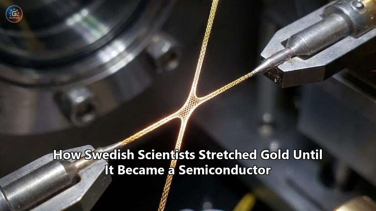
In April 2024, a team of materials physicists at Linköping University in Sweden published a paper in Nature Synthesis that quietly upended a foundational tenet of solid-state physics. Led by assistant professor Shun Kashiwaya and professor Lars Hultman, the researchers announced that they had synthesized "goldene"—the world’s first freestanding, single-atom-thick sheet of gold.
This achievement was far more than a triumph of extreme physical thinning. By restricting gold to a two-dimensional plane, the researchers altered its physical identity. In its three-dimensional, bulk form, gold is the quintessential metal: highly conductive, lustrous, ductile, and chemically inert. However, when stretched into a monolayer lattice just one atom thick, the material undergoes a dramatic transition, shedding its metallic character to become a semiconductor.
This development provides a lens through which we can analyze a broader, highly consequential pattern in modern materials science: the transition from compositional engineering to coordinate and dimensional engineering. Rather than synthesizing complex multi-element alloys to achieve specific electronic characteristics, researchers are increasingly utilizing spatial restriction and orbital manipulation of pure elements to manifest entirely new states of matter.
By analyzing the synthesis, physical mechanics, and structural lessons of goldene, we can extract critical principles that will govern the next generation of materials design, nanomanufacturing, and chemical catalysis.
The Physics of Dimensional Restriction: How Metals Transition to Semiconductors
To understand how a highly conductive metal can be coaxed into acting as a semiconductor, one must analyze the relationship between atomic coordination, orbital hybridization, and electronic band structure.
In bulk gold, atoms organize themselves into a face-centered cubic (FCC) crystal lattice. In this highly packed 3D configuration, each individual gold atom is surrounded by, and bonded to, 12 nearest neighbors—a coordinate number (CN) of 12. The valence electrons of these atoms reside in the $6s^1$ orbital, which sits atop a fully filled $5d^{10}$ shell. In the bulk state, these $6s$ wavefunctions overlap extensively, creating a highly delocalized "electron sea."
Because these electronic bands overlap continuously across the Fermi level without any energy gaps, electrons require virtually no thermal or electrical excitation to move through the crystal. This is the quantum mechanical origin of gold's exceptional electrical and thermal conductivity.
Bulk Gold (3D FCC)             Goldene (2D Monolayer)
   CN = 12                         CN = 6
  [   Au   ]                      [   Au   ]
 /  / | \  \                     /    |    \
O  O  O  O  O                   O     O     O
 |  |  X  |  |
O  O  O  O  O                   No out-of-plane bonds
(Continuous overlapping bands)  (Discretized bands / Bandgap opens)
When this structure is restricted to a single atomic layer, this coordinate environment collapses. In 2D goldene, each gold atom is restricted to a planar hexagonal sheet, reducing its coordination number from 12 to just 6. This reduction fundamentally reorganizes the electrostatic potential of the crystal lattice, leading to three primary physical consequences:
- Lattice Contraction: With only half of its original nearest neighbors, the remaining in-plane bonds must compensate for the missing out-of-plane electronic interactions. This causes a dramatic strengthening of the in-plane bonds, resulting in a lattice contraction of approximately 9% compared to bulk gold.
- Orbital Rehybridization: In bulk gold, the $5d$ and $6s$ orbitals hybridize in a manner that keeps the $5d$ band completely below the Fermi level while the $6s$ band remains half-filled and highly conductive. In the 2D configuration, the contraction of the lattice and the loss of vertical symmetry force a dramatic splitting of the $5d$ states. These $5d$ states hybridize strongly with the $6s$ and $6p$ states, shifting the relative energy levels of the bonding and anti-bonding orbitals.
- Quantum Confinement: Restricting electron wavefunctions to a plane thinner than the de Broglie wavelength of the conduction electrons discretizes the continuous energy bands seen in bulk materials.
This combination of orbital rehybridization and quantum confinement results in the opening of an electronic bandgap. The energy states near the Fermi level are no longer continuous; instead, a forbidden energy region is established. This means that electrons can no longer move freely under the slightest applied voltage. They instead require a specific packet of energy to jump from the newly formed valence band (dominated by filled $d$-states) to the conduction band (dominated by empty $sp$-states).
By compressing the material to its absolute physical limit, the Swedish research team successfully modified the electronic band structure of 2D goldene, allowing researchers to study and manipulate gold semiconductor properties. Unlike graphene, which is a zero-bandgap semimetal, goldene behaves as a true semiconductor.
This transition is further influenced by relativistic effects. Because gold is a heavy element ($Z = 79$), the inner-shell $1s$ electrons travel at a significant fraction of the speed of light. This causes a relativistic mass increase, which in turn contracts the $s$ and $p$ orbitals while electrostatically shielding and expanding the $d$ and $f$ orbitals. In 2D goldene, these relativistic orbital alterations are laid bare, directly contributing to the stabilization of the 2D lattice and the emergence of unique gold semiconductor properties that differ from lighter transition metals.
The Accidental Discovery: Precursor MAX Phase and Intercalation Mechanics
The pathway to synthesizing goldene was not paved by a straightforward, top-down engineering plan. Instead, it was discovered through a sequence of serendipitous experimental anomalies—a pattern common to many of history's most notable material breakthroughs.
For years, the thin-film physics group at Linköping University had been global leaders in the study of MAX phases. MAX phases are a family of ternary, nanolaminated carbides and nitrides defined by the general formula $M_{n+1}AX_n$, where:
- M is a transition metal (such as titanium, scandium, or vanadium),
- A is an element from groups 12 to 16 of the periodic table (such as silicon, aluminum, or gallium),
- X is either carbon or nitrogen ($n = 1, 2, \text{or } 3$).
These materials exhibit an intriguing blend of metallic and ceramic properties: they are highly electrically conductive, thermal-shock resistant, and structurally robust.
MAX Phase Precursor (Ti3SiC2)         Intercalation (High-Temp Au Diffusion)
       [ Titanium Carbide ]                  [ Titanium Carbide ]
       [   Silicon Layer  ]   ===> Gold ===> [    Gold Layer    ] (Goldene Precursor)
       [ Titanium Carbide ]                  [ Titanium Carbide ]
                                             (Silicon leaves as vapor/reaction product)
The Swedish team’s original objective was to develop high-temperature stable electrical contacts. They began their experiments with titanium silicon carbide ($Ti_3SiC_2$), a well-known MAX phase featuring atomic monolayers of silicon sandwiched between rigid titanium carbide matrices. To establish a low-resistance electrical contact, they deposited a thin film of gold onto the surface of the $Ti_3SiC_2$ ceramic and subjected the assembly to high-temperature annealing.
At elevated temperatures, an unexpected solid-state diffusion event occurred. Rather than remaining on the surface as a distinct metallic contact layer, the gold atoms began to migrate deep into the ceramic lattice. The thermodynamic driving forces at high temperatures caused the silicon atoms within the $Ti_3SiC_2$ matrix to de-intercalate, diffusing out of the material. Simultaneously, the migrating gold atoms slipped into the vacant atomic planes left behind by the departing silicon.
This auto-substitution process, known as intercalation, resulted in a new nanolaminated material: titanium gold carbide ($Ti_3AuC_2$). In this compound, single-atom-thick sheets of pure gold were securely sandwiched between layers of titanium and carbon.
The Swedish team had created the precursor to goldene by accident. However, they faced a daunting materials science bottleneck: the gold monolayer was locked inside a highly stable, chemically resistant ceramic matrix. Extracting this atom-thick sheet of gold without destroying it or causing it to aggregate back into its 3D bulk state would require looking beyond traditional nanotechnology toolkits.
Bridging Antiquity and Nanotechnology: The Japanese Blacksmithing Etching Method
To isolate the embedded goldene sheets, the Linköping team had to solve a fundamental thermodynamic challenge: "metals do not like to be lonely".
In solid-state chemistry, metallic elements exhibit high surface energies. When metal atoms are stripped of their surrounding coordinates, they naturally seek to minimize their surface area-to-volume ratio. This thermodynamic drive leads to immediate coalescence or "island growth" (Volmer-Weber growth), where individual atoms clump together to form 3D nanoparticles. Traditional chemical exfoliation methods—such as using highly concentrated hydrofluoric acid (HF) to etch away transition-metal layers, a process commonly used to synthesize 2D MXenes—are far too aggressive for noble metals. An HF-based approach would either dissolve the entire structure or cause the freed gold atoms to immediately clump into bulk nanoparticles.
The solution came from an unexpected source: a century-old etching technique used by Japanese art smiths. Lars Hultman, searching for a selective etchant that could dissolve titanium carbide without touching gold, discovered Murakami’s reagent. Historically, Japanese blacksmiths used this specific chemical mixture to etch away carbon deposits and bring out the distinct crystalline patterns on the surfaces of hand-forged steel knives and swords.
Murakami's reagent is an aqueous solution composed of:
- Potassium ferricyanide ($K_3[Fe(CN)_6]$)
- Sodium hydroxide ($NaOH$)
In this alkaline mixture, the ferricyanide acts as a selective oxidizing agent. When applied to $Ti_3AuC_2$, the reagent selectively oxidizes and dissolves the titanium and carbon atoms in the flanking $Ti_3C_2$ layers, converting them into soluble complexes while leaving the noble gold layer chemically untouched.
Chemical Exfoliation Process:

   Ti3AuC2 Matrix               Murakami's Reagent                Freestanding Goldene
 [ Titanium Carbide ]             (Dark Environment)              \ \ \ \ \ \ \ \ \ \ \
 [    Gold Layer    ]  =========> Selective Oxidation  =========> [  Cysteine Surfactant  ]
 [ Titanium Carbide ]            of Titanium & Carbon             [  Single-Atom Gold  ]
                                                                  \ \ \ \ \ \ \ \ \ \ \
To translate this historical blacksmithing technique into a precise, reproducible nanolithographic process, Shun Kashiwaya spent months refining the reaction parameters. He experimented with varying concentrations of Murakami's reagent and different etching durations, discovering that a low concentration combined with an extended reaction time yielded the most stable sheets.
Critically, Kashiwaya realized that the chemical etching must be performed in complete darkness. Potassium ferricyanide is photochemically active; when exposed to light, the compound degrades, releasing free cyanide ions into the solution. Because free cyanide is one of the few chemical species capable of rapidly complexing with and dissolving gold, any ambient light during the etching process would destroy the emerging goldene sheets.
Once the surrounding titanium carbide layers were etched away, the team faced a final obstacle: preventing the isolated, freestanding goldene sheets from curling up or collapsing into 3D clumps. To resolve this, they introduced a surfactant—specifically cysteine, an amino acid containing a highly reactive thiol (sulfur-bearing) group—into the solution.
The sulfur atoms in the cysteine molecules formed strong covalent bonds with the coordinate-unsaturated gold atoms on both faces of the goldene sheet. The hydrophilic "tails" of the cysteine molecules extended outward into the aqueous solution, creating a steric and electrostatic barrier. This surfactant-mediated stabilization kept the goldene sheets suspended, flat, and isolated in the liquid, much like "cornflakes in milk".
Through this combination of solid-state ceramic engineering, ancient Japanese metallurgy, and modern surfactant chemistry, the Linköping team successfully isolated stable, freestanding goldene sheets up to 100 nanometers in lateral size.
Deconstructing the Case Study: Strategic Lessons for Modern Materials Design
The successful synthesis of goldene is not an isolated scientific curiosity. Rather, it serves as a highly informative case study that illustrates the shifting methodologies of modern materials science. By analyzing the decisions and physical realities of this breakthrough, we can extract three core design principles that are directly applicable across the broader landscape of nanotechnology, semiconductor engineering, and chemical synthesis.
       ┌────────────────────────────────────────────────────────┐
       │             Core Lessons of the Goldene Case           │
       └───────────────────────────┬────────────────────────────┘
                                   │
         ┌─────────────────────────┼─────────────────────────┐
         ▼                         ▼                         ▼
┌──────────────────┐      ┌──────────────────┐      ┌──────────────────┐
│   Coordination   │      │   Methodological │      │ Kinetic Arrest   │
│   Engineering    │      │    Integration   │      │  via Surfactants │
└────────┬─────────┘      └────────┬─────────┘      └────────┬─────────┘
         │                         │                         │
         ▼                         ▼                         ▼
  CN 12 to CN 6;           Ancient chemistry        Preventing natural
  opens bandgap            solves advanced          desire of metals
  without doping.          nano-bottlenecks.        to form 3D clumps.
Lesson 1: The Shift from Compositional to Coordination Engineering
Historically, the search for new semiconductors focused on compound synthesis. If a researcher needed a material with a specific bandgap, they would synthesize binary, ternary, or quaternary compounds (such as gallium arsenide, indium phosphide, or transition metal dichalcogenides), carefully balancing the stoichiometry of different elements to tune the electronic states.
The goldene case study highlights an alternative approach: Coordination Engineering. Rather than changing the chemical composition of the system, researchers can manipulate the physical properties of a pure element by systematically reducing its coordination number.
| Material Form | Coordination Number | Crystal Structure | Electronic Behavior | Primary Application |
|---|---|---|---|---|
| Bulk Gold | 12 | Face-Centered Cubic (FCC) | Metal (Excellent conductor) | Interconnects, contacts, reflective coatings |
| Goldene | 6 | Hexagonal Monolayer | Semiconductor (Finite bandgap) | Catalysis, optoelectronics, gas sensing |
By dropping the coordinate number from 12 to 6, the electronic states of gold are compressed and split, creating a bandgap without requiring any chemical dopants or foreign elements. This principle opens up a vast, unexplored landscape of monoelemental 2D materials (sometimes called "metallenes").
If gold can be transitioned from a conductor to a semiconductor purely through coordinate restriction, a similar approach could be applied to other noble and transition metals (such as silver, copper, platinum, and palladium), revealing a family of stable, single-element semiconductors with highly tunable electronic properties.
Lesson 2: Methodological Integration: Retrofitting Antiquity
The second major lesson from the goldene synthesis is the value of cross-disciplinary, historical methodology. Modern nanoscience often suffers from a form of technological chauvinism, where researchers assume that the solutions to cutting-edge physical problems must rely on increasingly complex, expensive, and high-energy equipment (such as extreme ultraviolet lithography, plasma etching, or molecular beam epitaxy).
The Linköping team bypassed a seemingly insurmountable nanotechnology bottleneck—the selective removal of a nanolaminated carbide layer without damaging an intercalated noble metal—by adopting a 100-year-old chemical reagent from traditional Japanese blacksmithing.
This demonstrates that historical metallurgical and chemical processes, developed over centuries of trial-and-error by artisans, often possess a level of chemical selectivity that can be highly useful in modern nanotechnology. By retrofitting ancient chemistry to modern solid-state precursors, materials scientists can discover elegant, low-energy, wet-chemical pathways that are inherently more scalable than high-vacuum physical processing methods.
Lesson 3: Kinetic Arrest of Thermodynamic Desires
In the synthesis of low-dimensional materials, thermodynamics is often the enemy. Nature is driven to maximize entropy and minimize free surface energy, which translates to a strong driving force for 2D metal monolayers to clump into 3D nanoparticles.
The goldene case study teaches us how to design and utilize kinetic arrest. The Swedish researchers did not attempt to find an environment where a single layer of gold was the absolute thermodynamic minimum. Instead, they designed a multi-step pathway that utilized a metastable state, then selectively removed the matrix while instantly freezing the gold atoms in place using a tailored surfactant.
The use of cysteine is a prime example of this strategy. The cysteine molecules do not merely coat the gold; they chemically bind to the coordinate-unsaturated surface bonds, effectively "capping" the thermodynamic drive of the gold atoms to search for other gold atoms. This chemistry acts as a thermodynamic brake, arresting the system in a metastable, 2D configuration indefinitely.
This principle of surfactant-mediated kinetic stabilization is a critical blueprint for the synthesis of any non-van der Waals 2D material, where the parent bulk crystal does not naturally possess weak interlayer forces.
Industrial and Strategic Implications of Goldene
The realization of goldene and the ability to control gold semiconductor properties has profound implications across multiple high-tech industries. By transitioning gold from an inert bulk conductor to a highly reactive 2D semiconductor, researchers have unlocked a suite of capabilities that could address key bottlenecks in clean energy, chemical processing, and microelectronics.
                     ┌────────────────────────────────────────────────────────┐
                     │          Applications of 2D Goldene Properties         │
                     └───────────────────────────┬────────────────────────────┘
                                                 │
         ┌───────────────────────────────────────┼───────────────────────────────────────┐
         ▼                                       ▼                                       ▼
┌──────────────────┐                    ┌──────────────────┐                    ┌──────────────────┐
│   Green Energy   │                    │     Precision    │                    │ Microelectronics │
│   & Catalysis    │                    │     Sensing      │                    │  & Photonics     │
└────────┬─────────┘                    └────────┬─────────┘                    └────────┬─────────┘
         │                                       │                                       │
         ▼                                       ▼                                       ▼
  Water splitting (H2);                   High surface area;                     Tunable bandgap;
  highly efficient CO2                    active sites detect                    plasmonics enable
  to fuel conversion.                     trace biomolecules.                    novel optodevices.
1. Advanced Chemical Catalysis and Clean Energy
One of the most immediate and economically viable applications of goldene lies in green chemistry and renewable energy production.
Gold nanoparticles are already widely used as catalysts in industrial chemistry. However, bulk gold is relatively inert, and nanoparticle catalysts utilize only a small fraction of their total gold atoms—specifically, those exposed on the outer surface. The vast majority of the expensive gold atoms remain locked inside the inactive core of the nanoparticle.
Goldene completely resolves this efficiency bottleneck. Because it is only a single atom thick, every single gold atom is exposed to the environment, resulting in a 100% surface-atom efficiency.
Furthermore, because 2D goldene is coordinate-unsaturated—having only 6 nearest neighbors instead of 12—each gold atom possesses "free bonds" that are highly chemically reactive. This unique electronic configuration makes goldene a highly active catalyst for several key chemical transformations:
- Carbon Dioxide Conversion: Goldene’s electronic structure is highly optimized for lowering the activation energy required to reduce $CO_2$. It can selectively convert carbon dioxide into valuable value-added chemicals and fuels, such as methanol, ethanol, or methane, providing a scalable pathway for carbon capture and utilization (CCU) technologies.
- Hydrogen Production (Water Splitting): In electrochemical hydrogen-generating catalysis, goldene can serve as an exceptionally efficient electrocatalyst. The high density of active atomic sites accelerates the hydrogen evolution reaction (HER), allowing for the clean generation of hydrogen fuel from water at a fraction of the precious-metal mass currently required by platinum-based catalysts.
- Water Purification: The high surface reactivity of goldene can be utilized to selectively adsorb and decompose organic pollutants, heavy metals, and micro-toxins in water filtration systems.
2. High-Performance Chemical and Biological Sensors
The electrical conductivity of a semiconductor is highly sensitive to its local chemical environment. Because goldene has a finite bandgap and a 100% exposed surface area, the adsorption of even a single foreign molecule onto its lattice can cause a measurable shift in its electrical resistance and optical profile.
This makes goldene an exceptional candidate for trace gas sensors, environmental monitors, and medical diagnostics.
For example, in medical biosensors, goldene sheets can be functionalized with specific antibodies or DNA single strands. When target biomarkers—such as cancer-indicative proteins or viral RNA—bind to the goldene surface, the charge transfer between the molecule and the 2D lattice alters the gold semiconductor properties, triggering an instant, highly sensitive electronic readout.
3. Optoelectronics, Photonics, and Communication
In its bulk form, gold interacts strongly with light through surface plasmon resonance—a collective oscillation of free conduction electrons. In 2D goldene, these plasmonic properties are constrained to a single plane and integrated with the material's semiconductor bandgap.
This integration of plasmonics and semiconductivity enables several unique optoelectronic capabilities:
- Solar Energy Harvesting: Goldene’s bandgap is highly tunable based on its local strain and substrate interaction. This allows it to absorb specific wavelengths of light across the solar spectrum, generating hot carriers that can be efficiently collected to drive photovoltaic cells with minimal thermalization losses.
- Plasmonic Photothermal Therapies: In medicine, goldene sheets can be directed to tumor sites. When illuminated with near-infrared (NIR) light, which easily penetrates human tissue, the goldene sheets undergo highly efficient plasmonic photothermal conversion. They convert light into localized heat, selectively destroying cancer cells without damaging surrounding healthy tissue.
- Next-Generation Photodetectors: Because goldene exhibits a fast electronic response time and strong light-matter interactions, it can be integrated into high-speed optoelectronic devices, serving as the active channel in photodetectors for optical fiber communications and quantum encryption systems.
Structural and Electronic Comparison of 2D Materials
To place goldene in its proper context within the broader landscape of nanotechnology, we must compare it with other foundational 2D materials. While graphene remains the benchmark for 2D structures, goldene offers several electronic and chemical profiles that are fundamentally distinct.
| Material | Atomic Structure | Bandgap (eV) | Electronic Type | Dominant Chemical Trait | Primary Technology Target |
|---|---|---|---|---|---|
| Graphene | Honeycomb Carbon (2D) | 0.0 (Zero bandgap) | Semimetal | Chemically stable, high carrier mobility | High-frequency transistors, structural composites, thermal management |
| Hexagonal Boron Nitride (h-BN) | Honeycomb Boron-Nitrogen (2D) | ~5.97 | Insulator | Highly inert, thermally stable | Dielectric layers, 2D material substrates, protective coatings |
| Transition Metal Dichalcogenides (TMDCs, e.g., MoS₂) | Transition Metal-Chalcogen Sandwich (3D-like 2D) | 1.2 to 2.5 (Direct in monolayer) | Semiconductor | Photoactive, moderate mobility | Flexible electronics, photodetectors, light-emitting diodes |
| Goldene | Hexagonal Monolayer Gold (2D) | ~0.95 to 2.85 (Substrate/solvent dependent) | Semiconductor | Ultra-high surface energy, coordinate-unsaturated active sites | Efficient green catalysis, optoelectronics, medical photothermal therapies |
Unlike graphene, which requires complex physical strain engineering or chemical functionalization to open a bandgap, goldene naturally exhibits semiconducting behavior due to its reduced coordination and lattice contraction.
Furthermore, while TMDCs like molybdenum disulfide ($MoS_2$) are chemically stable but possess lower electrical mobilities, goldene combines a tunable bandgap with the strong spin-orbit coupling and relativistic physics of a heavy noble metal. This makes goldene a unique candidate for spintronics—an emerging computing paradigm where information is processed using the spin of electrons rather than merely their charge.
Key Challenges, Technical Bottlenecks, and the Engineering Roadmap
While the laboratory synthesis of goldene is an undeniable milestone, transitioning this material from a liquid-suspended nanotech curiosity into a commercially viable industrial product requires overcoming several significant engineering bottlenecks.
Analyzing these challenges reveals the critical research roadmap that materials scientists and semiconductor manufacturers must follow over the next decade.
                  ┌────────────────────────────────────────────────────────┐
                  │             The Roadmap to Industrialization           │
                  └───────────────────────────┬────────────────────────────┘
                                              │
         ┌────────────────────────────────────┼────────────────────────────────────┐
         ▼                                    ▼                                    ▼
┌──────────────────┐                 ┌──────────────────┐                 ┌──────────────────┐
│   Scalability    │                 │   Environmental  │                 │    CMOS & Wafer  │
│    Bottleneck    │                 │     Stability    │                 │    Integration   │
└────────┬─────────┘                 └────────┬─────────┘                 └────────┬─────────┘
         │                                    │                                    │
         ▼                                    ▼                                    ▼
  Transition from                      Preventing 2D-to-3D                  Transferring sheets
  liquid flakes to                     collapse in ambient                  to substrates without
  continuous films.                    oxygen/moisture.                     defects or tearing.
Challenge 1: The Scalability Bottleneck
Currently, the synthesis method developed by the Linköping team yields small, isolated goldene flakes suspended in a wet-chemical surfactant solution. These flakes range in size from tens to a few hundred nanometers. While these dimensions are perfectly suited for laboratory characterization, electron microscopy, and liquid-phase catalysis, they are wholly inadequate for modern semiconductor manufacturing.
For industrial chip fabrication, materials must be deposited as continuous, highly crystalline, defect-free wafers up to 300 millimeters in diameter.
The current chemical exfoliation pathway is inherently batch-based and difficult to integrate into standard semiconductor line-production. To resolve this, researchers must develop alternative, gas-phase synthesis methods, such as Chemical Vapor Deposition (CVD) or Molecular Beam Epitaxy (MBE), to grow goldene directly onto targeted substrates.
However, growing a single-atom sheet of gold via vacuum-deposition methods is exceptionally difficult due to gold's high surface energy, which naturally drives the system toward island growth (Volmer-Weber mode) on most traditional substrates. Resolving this will require the discovery of novel "growth templates"—epitaxial substrates that possess a strong, matching crystalline symmetry with goldene, capable of stabilizing the monolayer during high-temperature gas-phase synthesis.
Challenge 2: Environmental Stability and Surfactant Removal
Goldene is a metastable material. It is held in its two-dimensional state only through its interactions with surrounding surfactant molecules (like cysteine) or rigid template materials.
If these surfactant molecules are removed to integrate the goldene sheet into an electronic device, the bare gold atoms, possessing two free chemical bonds, become highly reactive. When exposed to ambient air, moisture, or elevated temperatures, these uncoordinated gold atoms will rapidly react with oxygen or migrate toward one another, collapsing the 2D sheet into standard, 3D gold nanoparticles.
Developing methods to permanently stabilize goldene without degrading its electronic properties is a major research focus. Potential solutions include:
- Van der Waals Encapsulation: Sandwiching the goldene monolayer between two inert, atomically thin sheets of hexagonal boron nitride (h-BN) or graphene. This encapsulation protects the goldene sheet from environmental oxidation while maintaining its structural and electronic integrity.
- Chemical Passivation: Replacing temporary surfactant molecules with ultra-thin, highly stable organic or inorganic passivation layers that protect the active surface bonds without blocking the gold semiconductor properties.
Challenge 3: CMOS Foundry Integration and Contact Resistance
For goldene to be used in modern processors, it must be integrated into existing Complementary Metal-Oxide-Semiconductor (CMOS) fabrication facilities. This presents a physical and chemical hurdle:
        Typical CMOS Integration Defect Profile:

            [ Metal Contact (e.g., Titanium/Gold) ]
          ==================== INTERFACE ====================  <-- High Contact Resistance & Tearing
            [  Surfactant / Passivation Capping Layer  ]
            [        Goldene Semiconductor Monolayer   ]
[ Sapphire or Silicon Substrate ]- Contamination Risks: Semiconductor foundries are highly sensitive to precious metal contamination. Free gold atoms can diffuse rapidly into silicon, forming deep-level defect states that destroy transistor functionality. Introducing a gold-based 2D semiconductor into silicon foundries will require strict barrier engineering and dedicated processing lines.
- Transfer Technology: Wet-chemically exfoliated goldene must be transferred from its liquid growth solution onto silicon or sapphire wafers. This transfer process often introduces physical defects, such as wrinkles, tears, bubbles, and chemical impurities.
- Ohmic Contacts: Connecting a 2D semiconductor to external metallic circuits often results in high contact resistance due to the formation of a Schottky barrier at the interface. Developing low-resistance, ohmic contacts to an atom-thick goldene sheet is an unsolved solid-state engineering challenge.
Future Milestones: What to Watch For Next
As materials science moves deeper into the era of 2D monoelemental metals, several key milestones and upcoming developments will signal whether goldene can successfully transition from the laboratory bench to commercial technologies.
       ┌────────────────────────────────────────────────────────┐
       │               Future Milestones to Watch               │
       └───────────────────────────┬────────────────────────────┘
                                   │
         ┌─────────────────────────┼─────────────────────────┐
         ▼                         ▼                         ▼
┌──────────────────┐      ┌──────────────────┐      ┌──────────────────┐
│   Synthesis of   │      │   Wafer-Scale    │      │  Spintronic &    │
│  "Metallenes"    │      │   CVD Growth     │      │ Quantum Devices  │
└────────┬─────────┘      └────────┬─────────┘      └────────┬─────────┘
         │                         │                         │
         ▼                         ▼                         ▼
  Exfoliating silver,      Transitioning from        First prototypes
  copper, and platinum     micro-flakes to           utilizing spin-orbit
  using Murakami-style     continuous 300mm          splitting for
  reagents.                gasp-phase wafers.        logic gates.
1. The Synthesis of Silverene, Copperene, and Other Metallenes
The successful extraction of goldene has established a clear blueprint. Materials scientists are already exploring whether other noble and transition metals can be intercalated into MAX phases and selectively exfoliated.
Watch for the synthesis of "silverene" (2D silver) and "copperene" (2D copper) using similar Murakami-style selective etching reagents. Because silver and copper are lighter than gold, their relativistic orbital contractions are less severe, which will result in different bandgaps, carrier mobilities, and optical profiles. Developing a library of these 2D metals will provide engineers with an entire spectrum of single-element semiconductors to choose from.
2. The Realization of Wafer-Scale CVD Growth
The transition of goldene from liquid suspension to gas-phase CVD growth on rigid wafers is a critical milestone. Keep a close eye on publications describing the growth of goldene on template materials (such as graphene, silicon carbide, or molybdenum disulfide).
Once researchers can reliably grow continuous, square-centimeter-scale monolayers of goldene directly onto dielectric substrates, the door will open for the first prototype fabrication of goldene-based Field-Effect Transistors (FETs) and integrated optoelectronic chips.
3. Prototypes of Spintronic and Quantum Information Devices
Because gold is a heavy element with a strong spin-orbit interaction, 2D goldene is expected to exhibit significant spin-orbit splitting—a physical phenomenon where the spin states of conduction electrons are strongly coupled to their momentum.
Watch for the development of the first goldene-based spintronic devices, such as spin-valves and spin-orbit torque memories. These structures could enable microprocessors that process information using electron spin orientations, promising a massive reduction in power consumption and a dramatic increase in processing speeds compared to traditional silicon charge-based logic.
The synthesis of goldene by Swedish researchers is a vivid reminder that the properties of matter are not fixed. They are highly dynamic variables that can be modified by altering spatial dimensions, lattice coordination, and orbital environments. By stretching gold until it became a semiconductor, Lars Hultman, Shun Kashiwaya, and their team have not only fulfilled an alchemist's dream of modifying the nature of a noble element; they have established a compelling paradigm for the future of materials-by-design.
Reference:
- https://semiengineering.com/synthesis-of-goldene-comprising-single-atom-layer-gold-linkoping-university/
- https://www.nanotechnologyworld.org/post/a-single-atom-layer-of-gold-liu-researchers-create-goldene
- https://evertiq.com/news/55599
- https://www.livescience.com/chemistry/worlds-thinnest-gold-leaf-dubbed-goldene-is-just-1-atom-thick
- https://www.zmescience.com/science/chemistry/scientists-make-the-first-single-atom-thick-sheet-of-gold-its-called-goldene/
- https://pubs.acs.org/doi/10.1021/acsnano.0c06697
- https://www.thebrighterside.news/post/single-atom-thick-gold-goldene-opens-doors-to-a-clean-tech-revolution/
- https://ouci.dntb.gov.ua/en/works/4r3GkpYl/
- https://www.cas.org/resources/cas-insights/goldene
- https://pmc.ncbi.nlm.nih.gov/articles/PMC7203110/
- https://www.tomshardware.com/tech-industry/researchers-create-goldene-a-single-atomic-layer-of-gold-with-semiconductor-properties
- https://en.wikipedia.org/wiki/Two-dimensional_semiconductor
- https://liu.se/en/news-item/ett-atomlager-guld-liu-forskare-skapar-gulden
- https://www.chemeurope.com/en/news/1183256/a-single-atom-layer-of-gold.html
- https://pmc.ncbi.nlm.nih.gov/articles/PMC12985632/
- https://www.sciencenews.org/article/goldene-sheet-gold-one-atom-thick
- https://icmctf2026.avs.org/wp-content/uploads/2025/12/Abstract-Book.pdf
- https://www.legacyias.com/scientists-make-unique-2d-metals-much-sought-after-for-future-tech/
- https://www.insightsonindia.com/2025/05/15/2d-metal/
- https://spacedaily.com/research-discovery-could-revolutionise-semiconductor-manufacture-999/
- https://www.researchgate.net/publication/388257922_How_does_Goldene_Stack
- https://tavex.se/en/scientists-have-turned-lead-into-gold/