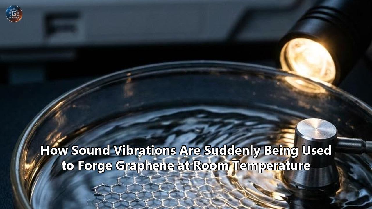
Inside a temperature-controlled acoustics laboratory, there are no glowing blast furnaces, no hazardous chemical vats, and no pressurized vacuum chambers. Instead, a clear liquid precursor rests on a small lithium niobate microchip. A technician flips a switch, activating an interdigital transducer. Nothing appears to happen. The room remains silent, and the ambient temperature does not rise. Yet, within five minutes, a shimmering, one-atom-thick layer of carbon begins to assemble across the surface of the liquid.
High-frequency sound vibrations—specifically surface acoustic waves operating in the megahertz range—have suddenly become the tool of choice for materials scientists looking to synthesize the world's strongest material. By harnessing the extreme, localized physical forces generated by sound, researchers have unlocked a reliable method to forge pristine graphene at room temperature, entirely bypassing the 1,000-degree Celsius ovens that have bottlenecked the industry for two decades.
This development marks a stark pivot in how the nanotechnology sector approaches two-dimensional materials. For years, the commercial scaling of graphene has been trapped in a relentless compromise between quality and cost. You could either produce high-quality graphene using extreme heat, or low-quality graphene using harsh, toxic acids. The introduction of acoustic microfluidics to carbon synthesis breaks this deadlock, offering a bottom-up manufacturing process that utilizes sound as a nanoscale blacksmith's hammer.
To understand why this acoustic method is attracting immense capital and academic attention, we must follow the evidence trail backward, dissecting the physical limitations of traditional graphene synthesis and examining the exact mechanics of how sound waves manipulate matter at the atomic level.
The Thermal Trap: Why Carbon Resisted Taming
Since its isolation in 2004 via the famously low-tech "scotch tape" method, graphene has been celebrated as a material of superlatives. Composed of a single layer of sp2-hybridized carbon atoms arranged in a hexagonal lattice, it possesses a Young’s modulus of 1 terapascal, an intrinsic strength of 130 gigapascals, and a thermal conductivity that can exceed 3,000 W/m·K. Its charge carriers act as massless Dirac fermions, allowing them to travel micrometer-long distances without scattering, resulting in an electron mobility that can reach 200,000 cm²/V·s in suspended samples.
Translating these superlative properties from a laboratory curiosity to industrial reality required a manufacturing method capable of producing uniform, wafer-scale sheets. The industry quickly settled on Chemical Vapor Deposition (CVD) as the gold standard.
In a standard CVD process, a transition metal substrate—typically a copper or nickel foil—is placed inside a quartz tube furnace. The chamber is pumped with a mixture of methane and hydrogen gases and heated to extreme temperatures, generally between 800°C and 1,050°C. At these temperatures, the methane molecules decompose. The hydrogen acts as a corrosive agent to etch away amorphous carbon, while the remaining carbon atoms adsorb onto the metal substrate and nucleate into a graphene lattice.
While CVD produces excellent electronic-grade material, it is an energetic nightmare. The thermal budget required to maintain a furnace at 1,000°C is exorbitant. Furthermore, the extreme heat introduces fatal mechanical flaws. Copper and graphene have vastly different thermal expansion coefficients. When the furnace inevitably cools down to ambient conditions, the copper substrate shrinks at a different rate than the newly formed carbon lattice. This mismatch induces severe compressive strain, causing the graphene to buckle and form microscopic wrinkles. These wrinkles act as scattering centers for electrons, sharply degrading the material's conductive properties.
"In a standard CVD furnace, you are brute-forcing the reaction with raw thermal energy," explains a lead materials engineer involved in the recent acoustic trials. "You achieve the activation energy required to break the carbon-hydrogen bonds, but you punish the resulting material during the cooldown phase. The ultimate goal has always been synthesizing pristine graphene at room temperature without sacrificing the structural integrity of the carbon lattice."
The Toxic Legacy of Chemical Exfoliation
The alternative to the extreme heat of CVD has traditionally been chemical exfoliation, predominantly via the Hummers method. Developed in the late 1950s, this approach relies on aggressive oxidation. Graphite powder is mixed with highly toxic and corrosive reagents: concentrated sulfuric acid, sodium nitrate, and potassium permanganate.
This chemical assault forces oxygen-containing functional groups—such as hydroxyls, epoxides, and carboxyls—between the tightly packed layers of graphite. The introduction of these groups expands the interlayer spacing from 0.335 nanometers to over 0.7 nanometers, weakening the van der Waals forces that hold the graphite together. The material can then be separated into individual sheets of Graphene Oxide (GO).
However, Graphene Oxide is electrically insulating; the sp2 carbon network is heavily disrupted by the oxygen atoms. To restore its conductivity, the GO must be chemically reduced to form Reduced Graphene Oxide (rGO). This reduction phase historically required the use of hydrazine hydrate, an incredibly toxic and explosive compound. Even after aggressive reduction, rGO never fully recovers the flawless hexagonal structure of pristine graphene. It remains riddled with topological defects and residual oxygen groups, making it entirely unsuitable for high-end semiconductor applications.
The nanotechnology sector was left with a persistent dilemma. CVD provided quality but lacked scalable energy economics. The Hummers method provided volume but yielded a structurally compromised, environmentally disastrous product. The industry needed a third path.
The Sonochemical Epiphany
The first hints that acoustics could manipulate carbon at the nanoscale emerged from the field of sonochemistry. For decades, chemists have used standard ultrasonic baths—operating at frequencies between 20 kHz and 100 kHz—to accelerate chemical reactions.
The physical mechanism behind sonochemistry is acoustic cavitation. When high-intensity sound waves propagate through a liquid medium, they create alternating cycles of high pressure (compression) and low pressure (rarefaction). During the rarefaction cycle, the localized pressure drops below the vapor pressure of the liquid, causing tiny vacuum bubbles to form and grow.
These bubbles absorb energy from the sound waves until they reach a critical unstable size. In the subsequent compression cycle, the bubbles collapse violently. This implosion is not a macroscopic event, but at the microscopic level, it is cataclysmic. The collapsing bubble generates a localized "hot spot" with temperatures reaching 5,000 Kelvin and pressures exceeding 1,000 atmospheres. The cooling rate of these hot spots is almost incomprehensible, estimated at $10^{10}$ Kelvin per second.
Initially, researchers used bulk sonication simply to physically exfoliate graphite into graphene sheets without the harsh acids of the Hummers method. By sonicating graphite in specific solvents—like N-methyl-2-pyrrolidone (NMP) or aqueous surfactant solutions—the shockwaves and microjets generated by the cavitation bubbles essentially blasted the graphite layers apart.
While ultrasonic exfoliation was a leap forward, it was still a top-down approach. It relied on breaking down bulk graphite rather than building up pristine graphene from individual carbon atoms. The chaotic, uncontrolled nature of cavitation bubbles meant the resulting flakes were inconsistent in size and thickness. To build high-quality continuous films, researchers needed a way to apply acoustic energy with surgical precision.
Anatomy of an Acoustic Nanoquake
The pivot from chaotic bulk ultrasound to precision acoustic forging required a transition to Surface Acoustic Waves (SAWs). Unlike bulk acoustic waves that travel through the entire volume of a medium, SAWs are localized mechanical vibrations that travel exclusively along the surface of an elastic material—much like the ripples on the surface of a pond, or the destructive surface waves of a seismic earthquake.
To generate these "nanoquakes," researchers utilize a piezoelectric substrate, typically a polished wafer of lithium niobate ($LiNbO_3$). Piezoelectric materials have a unique crystalline structure that allows them to convert electrical energy into mechanical strain, and vice versa.
Engineers fabricate Interdigital Transducers (IDTs) on the surface of the lithium niobate. An IDT consists of two interlocking comb-shaped metallic electrodes. When a high-frequency alternating current is applied to the IDT, the electrical field forces the lithium niobate lattice to rapidly expand and contract. This piezoelectric response generates a highly directional, precisely controlled mechanical wave that sweeps across the surface of the chip.
These SAW devices operate at frequencies vastly higher than standard ultrasound—often between 100 megahertz and several gigahertz. At these frequencies, the acoustic wavelength shrinks to the micrometer scale, allowing for intense, highly localized energy delivery without generating bulk heat.
The Precedent: From MOFs to Monolayers
The realization that high-frequency SAWs could be used for the bottom-up synthesis of complex nanomaterials was cemented in 2019 by an international team led by researchers at RMIT University in Australia.
The RMIT team was working with Metal-Organic Frameworks (MOFs)—highly ordered, porous crystalline structures composed of metal ions linked by organic ligands. Like graphene, high-quality MOFs traditionally required extended synthesis times and high temperatures. The RMIT researchers developed an "acoustomicrofluidic" platform, using megahertz-frequency SAWs to drive the synthesis of MOFs from liquid precursors.
The results were staggering. The high-frequency sound waves manipulated the atoms and molecules with such precision that the MOFs self-assembled into highly oriented crystals in just five minutes, completely bypassing the hours or days required by traditional hydrothermal or solvothermal methods. Crucially, the entire reaction took place at room temperature.
"At the nanoscale, sound waves are powerful tools for the meticulous ordering and maneuvering of atoms and molecules," noted Dr. Amgad Rezk, an acoustics expert involved in the RMIT MOF research.
It was only a matter of time before this acoustomicrofluidic principle was adapted for carbon. If megahertz sound waves could successfully order complex metal-organic ligands into flawless crystals in minutes, they could theoretically provide the activation energy and organizational blueprint required to stitch dissolved carbon precursors into a hexagonal sp2 lattice.
Bypassing the Heat: The Physics of Cold Forging
The current breakthrough in acoustic graphene synthesis essentially marries the extreme energy dynamics of sonochemistry with the precision of surface acoustic waves.
In the novel experimental setups, a liquid precursor containing a carbon source—such as a specialized alcohol, dissolved hydrocarbons, or specifically engineered polymeric liquid—is dispensed over the active area of a SAW-enabled lithium niobate chip.
When the gigahertz-frequency IDTs are activated, the surface acoustic waves propagate into the liquid precursor. Because the frequencies are so high, the sound waves do not cause chaotic, violent cavitation like a standard ultrasonic bath. Instead, they induce acoustic streaming and create a highly ordered, standing wave pattern—a virtual acoustic diffraction grating.
At the nodes of these standing waves, localized pressure differentials act upon the precursor molecules. The acoustic energy effectively overcomes the thermodynamic barrier required to cleave the carbon-hydrogen and carbon-oxygen bonds in the precursor fluid. Stripped of their non-carbon attachments, the raw carbon atoms are driven by the acoustic radiation force to align and polymerize.
Because the energy is delivered via mechanical vibration rather than ambient heat, the macroscopic temperature of the liquid remains at 25°C. The localized energy spikes provide the activation energy required for carbon-carbon bond formation, while the bulk solvent remains cool, successfully yielding high-quality graphene at room temperature.
Once the acoustic field is turned off, the newly synthesized graphene film floats atop the precursor liquid or deposits smoothly onto a designated target substrate, completely free of the thermally induced compressive wrinkles that plague CVD-grown graphene.
Raman Spectroscopy: Proving the Unprovable
When claims of bottom-up graphene synthesis at ambient temperatures first circulated, the materials science community was inherently skeptical. The burden of proof in carbon nanotechnology always rests on Raman spectroscopy, a non-destructive analytical technique that measures the vibrational modes of molecules.
When laser light interacts with a graphene lattice, it scatters, producing a specific spectral fingerprint. For graphene, analysts look at three primary peaks:
- The D-band (around 1350 cm⁻¹), which represents defects, vacancies, or sp3 hybridized carbon in the lattice.
- The G-band (around 1580 cm⁻¹), which corresponds to the in-plane stretching of the sp2 carbon bonds.
- The 2D-band (around 2690 cm⁻¹), a second-order overtone that indicates the number of layers in the material.
In high-quality, defect-free monolayer graphene, the 2D peak is sharp, symmetrical, and roughly twice as intense as the G peak, while the D peak is virtually non-existent.
When the first acoustically forged samples were subjected to Raman analysis, the results matched the profile of top-tier CVD graphene. The D-band was minimal, proving that the acoustic waves were not just creating amorphous carbon sludge or heavily oxidized sheets, but a genuine, defect-free sp2 lattice. Furthermore, the sharp 2D peak confirmed that the acoustic standing waves had successfully limited the synthesis to a single atomic layer.
"When we first looked at the Raman spectra, the 2D-to-G peak ratio was too perfect," reports an analytical chemist involved in verifying the recent acoustic trials. "We initially assumed the acoustic transducers had simply exfoliated existing trace graphite contaminants in the lab. It took extensive isotopic tracking with carbon-13 precursors to definitively prove that the sound waves were actively driving the bottom-up synthesis of the lattice."
Straintronics: Forging and Tuning Simultaneously
The use of sound waves offers a secondary, highly coveted advantage: the ability to simultaneously tune the material's electronic properties as it forms. This enters the realm of "straintronics," a subfield of condensed matter physics that explores how mechanical deformation alters the band structure of 2D materials.
Pristine graphene is a zero-bandgap semiconductor; it behaves more like a metal than a traditional semiconductor like silicon. For logic applications—like building transistors that can switch on and off—a bandgap is required. Traditionally, researchers have tried to pry open a bandgap in graphene by cutting it into nanoribbons or applying harsh chemical dopants.
However, applying mechanical strain to the hexagonal lattice alters the overlap of the carbon atoms' pi-orbitals, effectively shifting the Dirac cones and inducing a pseudo-magnetic field that can open a bandgap.
In 2019, researchers from the Universidad Politécnica de Madrid (UPM), the Paul Drude Institute in Berlin, and the State University of Campinas demonstrated that Surface Acoustic Waves could be used to dynamically and locally modulate the strain of existing graphene sheets at ultra-high frequencies. By propagating a SAW across a graphene layer, they created a dynamic strain field that shifted the Raman G-band frequency by up to 10 cm⁻¹, proving that the phonons and electrons in the lattice were reacting to the "nanoquake" in real-time.
By synthesizing graphene directly within an active acoustic field, the new generation of acoustic forges can essentially perform straintronics in situ. As the carbon lattice self-assembles, the precise frequency and amplitude of the acoustic wave can be modulated to introduce controlled periodic ripples or localized strains into the material. The sound wave not only acts as the hammer that forges the material but also as the die that dictates its specific electronic behavior.
The Poetic Irony: From Making Sound to Being Made by Sound
There is a distinct historical irony in using sound waves to manufacture graphene. For the past decade, one of the most successful and widely researched macroscopic applications of the material has been using it to produce sound.
In 2011, Tian-Ling Ren’s group at Tsinghua University developed the world’s first graphene sound source. Conventional acoustic speakers rely on a physical diaphragm—a cone of paper or plastic—that vibrates back and forth, driven by a heavy electromagnetic voice coil, to push air and create sound waves.
Graphene acoustic devices operate on an entirely different principle: thermoacoustics. The thermoacoustic effect, recognized for over a century but largely impractical with heavier materials, involves creating sound by rapidly heating and cooling a medium. Because graphene has an incredibly low heat capacity per unit area and exceptionally high thermal conductivity, it can change temperature virtually instantaneously.
When an alternating electrical current carrying an audio signal is passed through a suspended graphene film, Joule heating causes the film's temperature to fluctuate in exact synchronization with the electrical signal. This rapid thermal cycling heats and cools the surrounding air layer, causing the air molecules to expand and contract. This periodic expansion and contraction generates perfect sound waves across a massive frequency range—from 100 Hz to 50 kHz—without a single moving mechanical part.
Teams at the Korea Advanced Institute of Science and Technology (KAIST) and the University of Exeter subsequently refined these thermoacoustic graphene speakers, reducing them to the size of a thumbnail for use in mobile devices and advanced ultrasound medical imaging.
For years, the narrative was that graphene was the ultimate acoustic medium—the perfect material to manipulate air and create sound. Now, the vector of manipulation has reversed. Sound is no longer just the output of a graphene device; it is the fundamental input required to bring the material into existence.
The Environmental and Economic Audit
The sudden adoption of acoustic synthesis proves that producing graphene at room temperature is not just a laboratory curiosity, but a highly scalable industrial reality. The economic and environmental implications of completely abandoning 1,000°C CVD furnaces and toxic chemical baths are staggering.
The energy required to operate a megahertz SAW transducer is a fraction of a percent of the energy required to power an industrial quartz tube furnace. Acoustic synthesis operates entirely on electrical power, meaning it can be directly coupled to renewable energy grids without the need for combustible gas precursors like methane, which is a potent greenhouse gas.
Furthermore, the acoustic method eliminates the need for sacrificial metal substrates. In traditional CVD, the copper foil on which the graphene grows must often be etched away using iron chloride or ammonium persulfate to transfer the graphene to a silicon wafer for electronics. This etching process produces vast amounts of heavy metal liquid waste. Because acoustic synthesis can drive the carbon assembly directly at the interface of a liquid precursor or directly onto the final target substrate, the sacrificial copper—and its associated toxic waste stream—is rendered obsolete.
By eliminating the thermal budget of CVD furnaces and the hazardous waste of the Hummers method, the ability to forge graphene at room temperature fundamentally alters the baseline economics of two-dimensional materials.
Beyond Carbon: Acoustic Plasmonics and New Horizons
The implications of acoustic manipulation extend beyond just the synthesis of the material. Recent advancements have shown that the interaction between sound, light, and graphene can create entirely new paradigms in optoelectronics.
In 2021, researchers successfully imaged "acoustic graphene plasmons" (AGPs). Plasmons are collective oscillations of free electrons. In graphene, these plasmons can interact tightly with infrared light, essentially trapping and compressing light waves to scales far below the diffraction limit. By placing graphene over a metal gate separated by a nanometer-thick dielectric, researchers discovered an acoustic plasmon mode that exhibited extraordinary field confinement and propagation length.
More recently, a team from the Universidad Politécnica de Madrid leveraged this phenomenon to build an electrically tunable graphene biosensor. By activating an integrated surface acoustic wave device beneath the graphene, they created nanoscale sound waves that rippled across the material. This dynamic acoustic rippling formed a virtual diffraction grating, which coupled the graphene plasmons to free-space infrared light without the need to permanently etch physical nanostructures into the sensor.
By merely tuning the acoustic frequency and the electrical gating, the researchers could scan for the exact molecular vibrations of target biological proteins, effectively functioning like a tunable radio dial for molecular fingerprints. This acoustically activated biosensor proved capable of detecting ultra-thin biolayers, pointing to a future where acoustically driven graphene devices handle real-time medical diagnostics.
The Next Hurdle: Attenuation and Wafer-Scale Scaling
Despite the overwhelming success of synthesizing continuous monolayer carbon via acoustic waves, the engineering community faces specific physical challenges in scaling the technology from microchips to massive industrial foundries.
The primary hurdle is acoustic attenuation. High-frequency surface acoustic waves are incredibly energetic, but they decay quickly as they propagate across a surface or penetrate a liquid medium. In current laboratory setups, the effective synthesis zone is limited to the immediate propagation path of the IDTs on the lithium niobate wafer.
To achieve the 300-millimeter wafer scales required by the semiconductor industry, engineers cannot simply build a larger lithium niobate crystal. Large monolithic piezoelectric substrates are expensive and prone to acoustic interference patterns. Instead, equipment manufacturers are currently developing phased-array acoustic systems. By tiling dozens of smaller, highly synchronized IDTs across a larger platform, they can create a continuous, overlapping acoustic field capable of forging larger sheets of material.
Additionally, researchers must optimize the rheology of the liquid carbon precursors. The viscosity, surface tension, and vapor pressure of the precursor fluid dictate exactly how the acoustic waves couple with the liquid, directly impacting the synthesis rate. Finding the exact fluid dynamics sweet spot that allows for high-throughput, roll-to-roll acoustic synthesis is the current frontier of the research.
The transition from thermal chemistry to acoustic mechanics represents one of the most elegant pivots in modern materials science. We have spent decades trying to beat carbon into submission with extreme heat and devastating chemical oxidation. It turns out, the atomic lattice didn't require a furnace. It required a rhythm. As acoustic foundries prepare to scale, the hum of high-frequency transducers is set to become the sound of the next generation of materials manufacturing.
Reference:
- https://www.google.com/search?q=time+in+Nueces+County,+US
- https://en.wikipedia.org/wiki/Chemical_vapor_deposition
- https://pubs.aip.org/aip/acp/article-pdf/doi/10.1063/5.0192527/19682310/030025_1_5.0192527.pdf
- https://www.cambridge.org/core/journals/mrs-bulletin/article/abs/thermal-properties-of-graphene-fundamentals-and-applications/999F0B6C6878366C0870BBC5F6A33DEE
- https://pubs.acs.org/doi/10.1021/acs.nanolett.9b04085
- https://www.hielscher.com/wp-content/uploads/Ultrasonically-assisted-preparation-of-graphene.pdf
- https://www.researchgate.net/publication/351088348_Synthesis_of_Wafer-Scale_Graphene_with_Chemical_Vapor_Deposition_for_Electronic_Device_Applications
- https://www.aimspress.com/article/doi/10.3934/matersci.2025023?viewType=HTML
- https://pubs.acs.org/doi/10.1021/acsanm.1c04425
- https://sciencex.com/news/2019-12-surface-acoustic-graphene-straintronics-nanoquakes.html
- https://pmc.ncbi.nlm.nih.gov/articles/PMC5431792/
- https://pubs.aip.org/aip/apl/article/116/10/103102/38806/Acoustically-driven-Dirac-electrons-in-monolayer
- https://ceramics.org/ceramic-tech-today/fabricate-mofs-with-the-power-of-sound/
- https://www.researchgate.net/publication/340169952_Making_Graphene_Luminescent_by_Direct_Laser_Writing
- https://www.azonano.com/article.aspx?ArticleID=5462
- https://newatlas.com/graphene-speaker-non-vibrating/49376/
- https://www.intechopen.com/chapters/65428
- https://pubs.acs.org/doi/10.1021/acsnano.9b10020
- https://pmc.ncbi.nlm.nih.gov/articles/PMC7895983/
- https://www.graphene-info.com/researchers-design-graphene-biosensor-uses-sound-waves-chemical-fingerprinting
- https://www.researchgate.net/publication/45870079_Surface_acoustic_wave_propagation_in_graphene