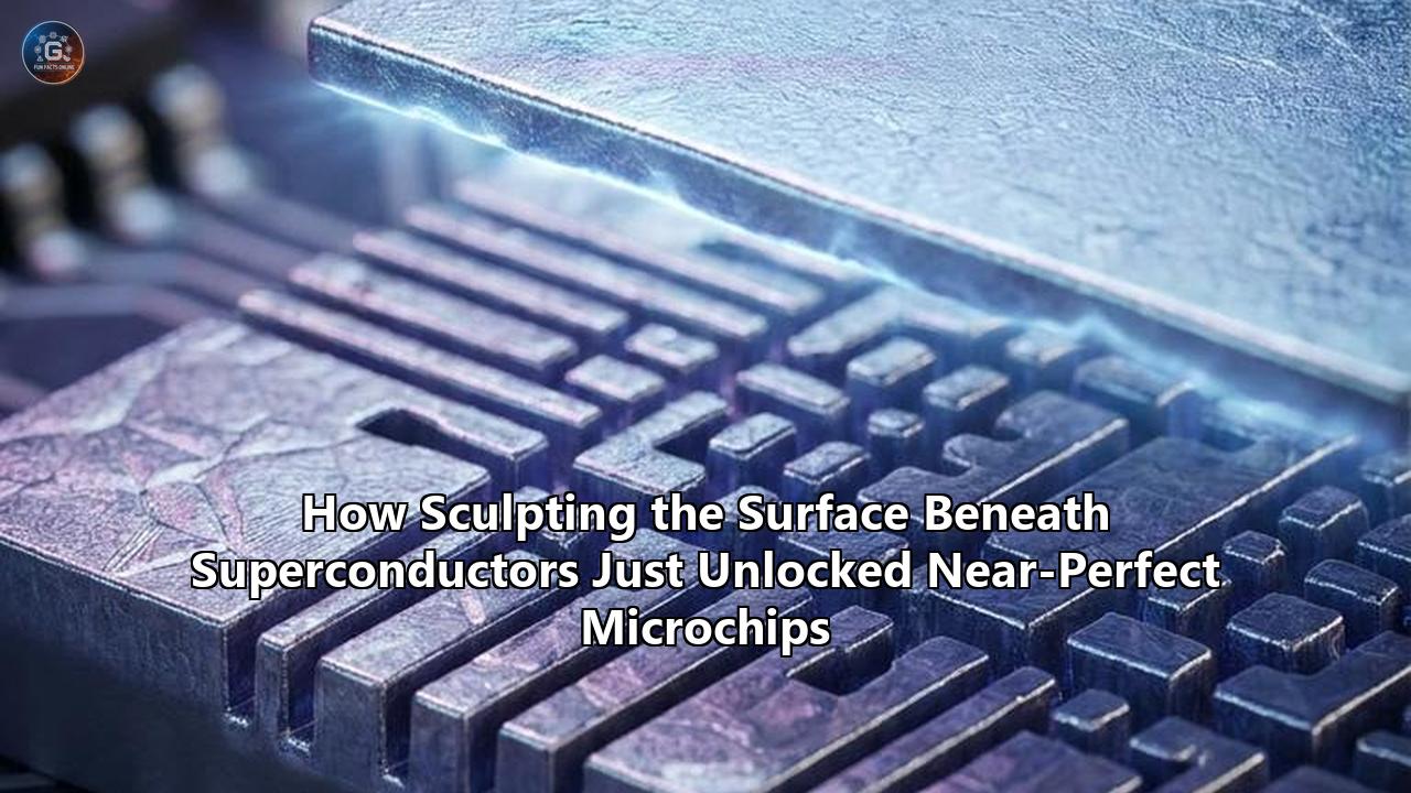
On June 17, 2026, a research team at the Chalmers University of Technology in Sweden published a study in Nature Communications that bypassed a decades-old bottleneck in solid-state physics. Led by Dr. Floriana Lombardi, a professor of Quantum Device Physics, the researchers demonstrated that by subtly "sculpting" the nanoscale surface of the substrate beneath an ultrathin superconducting film, they could dramatically enhance its superconducting properties.
Instead of synthesizing new exotic chemical compounds or manipulating the superconductor directly, the Chalmers team pretreated a magnesium oxide (MgO) substrate in a high-temperature vacuum. This process forced the substrate to self-assemble into a regular, undulating pattern of triangular "nanofacets" measuring just 1 nanometer tall and 20 to 50 nanometers wide.
When an ultrathin film of yttrium barium copper oxide (YBCO)—a high-temperature cuprate superconductor—was deposited on top of this textured surface, the atomic-scale ridges and valleys guided how the YBCO atoms settled. This engineered atomic arrangement induced a directional electronic state at the interface.
The results were immediate: the superconducting onset temperature rose by more than 15 Kelvin, and the material’s upper critical magnetic field—the threshold at which superconductivity collapses—shot up by more than 50 tesla compared to flat reference films.
This development represents a turning point in superconductor microchip technology. For years, scientists have struggled to integrate superconducting circuits into classical and quantum computing architectures because of two fundamental flaws: the requirement for near-absolute-zero cooling and an extreme vulnerability to ambient magnetic fields. By shifting the engineering focus from the superconducting material itself to the topography of the substrate beneath it, this "sculpted surface" technique opens a new frontier in microfabrication.
Yet, this geometric approach is not the only strategy vying to redefine high-performance microchips. Across the global research landscape, a series of competing philosophies have emerged. Some physicists are championing radical new material substitutions, others are chemically etching the substrate away entirely to suspend circuits in mid-air, and a few are experimenting with 3D-printed superconducting meshes.
Evaluating how these diverse approaches compare, contrast, and clash reveals the unique trade-offs defining the race for the near-perfect microchip.
The Physics of Interfaces: Why Superconductor Microchip Technology Has Been Stalled
To appreciate why sculpting the substrate is a departure from historical norms, one must understand the underlying solid-state physics of superconducting interfaces.
In a conventional conductor, like copper or gold, electricity is carried by individual electrons that bounce off impurities, defects, and thermal vibrations in the material's crystal lattice. This scattering creates electrical resistance, which dissipates energy as waste heat.
In a superconductor, however, electrons pair up into states called Cooper pairs. Operating as a single, coherent quantum wave, these Cooper pairs glide through the crystal lattice without scattering, resulting in zero electrical resistance.
Conventional Conductor:
[Electron] ---> (Impurities / Defect) ---> Scattering (Resistance & Heat)

Superconductor:
[Electron = Electron] (Cooper Pair) --------> Zero Resistance / Unimpeded Flow
However, this collective quantum state is incredibly fragile. The glue that holds Cooper pairs together is weak, and it can easily be torn apart by two primary enemies:
- Thermal Energy: Heat causes the crystal lattice to vibrate violently, breaking the Cooper pairs.
- Magnetic Fields: Magnetic flux lines penetrate the superconductor, creating tiny whirlpools of normal current called vortices, which destroy the zero-resistance state.
For decades, the field of superconductor microchip technology has sought to build chips that utilize these properties for ultra-low-power, hyper-fast classical logic or as qubits for quantum computers. But when these circuits are shrunk down to the nanoscale, a new problem emerges: the interface.
When an ultrathin superconducting film is deposited onto a flat substrate—such as silicon, sapphire, or magnesium oxide—the boundary between the two materials is rarely perfect. The atoms of the superconductor try to align with the atoms of the substrate, but because their natural crystal lattice spacings do not match, the film experiences immense mechanical strain.
This strain distorts the superconductor’s atomic structure, degrading its ability to conduct without resistance. Furthermore, the flat interface acts as a breeding ground for "two-level system" (TLS) defects—microscopic dangling bonds, oxygen vacancies, and chemical impurities that trap energy and cause quantum decoherence.
Historically, researchers tried to solve this by searching for better superconducting compounds or by using complex chemical doping. The Chalmers breakthrough flips this paradigm by demonstrating that the substrate is not merely a passive holder for the circuit; it is an active tuning knob.
Comparing the Contenders: Four Paths to Perfect Microchips
As the semiconductor industry hits the physical limits of classical silicon scaling, several competing methodologies are attempting to resolve the interface bottleneck. Each approach represents a fundamentally different engineering philosophy, balancing performance, scalability, and material complexity.
| Metric / Feature | Substrate Sculpting (Chalmers) | Material Substitution (Princeton) | Air-Suspension Etching (Berkeley Lab) | 3D-Printed Porous Nitrides (Cornell) |
|---|---|---|---|---|
| Primary Mechanism | Nanofaceted substrate patterns guide atomic growth | Swapping metals (Tantalum) and optimizing silicon interfaces | Chemical etching of substrate to suspend circuits in air | Additive 3D printing of copolymer-nanoparticle inks |
| Material System | YBCO on Magnesium Oxide (MgO) | Tantalum on Silicon (Si) | Aluminum on Silicon (Si) | Crystalline Nitrides (e.g., Titanium Nitride) |
| Key Performance Metric | +15 K critical temp; +50 T magnetic limit | >1 millisecond qubit coherence (15x industry standard) | Significant reduction in dielectric loss and substrate noise | Record-breaking surface area for compound superconductors |
| Target Application | High-temp power electronics, high-field quantum sensors | Scalable quantum computing processors (QPUs) | Noise-resistant quantum bits (qubits) | Quantum hardware, advanced sensors, catalyst templates |
| CMOS Compatibility | Low (requires high-temp vacuum & exotic MgO) | High (uses standard silicon wafers and CMOS tools) | Moderate (requires post-processing chemical etching steps) | Very Low (additive printing is fundamentally non-planar) |
| Mechanical Stability | High (fully supported solid-state film) | High (standard planar solid-state chip) | Low (suspended nanostructures are fragile) | Moderate (porous structure; requires careful thermal processing) |
Path A: Substrate Sculpting (The Chalmers Geometrical Force)
The core innovation of the Chalmers University of Technology approach lies in its use of geometry over chemistry. In their YBCO-on-MgO system, the YBCO is a high-temperature cuprate. Cuprates are notorious for being structurally rigid and chemically delicate; once they are fabricated, their electronic properties are essentially locked in place.
By pre-treating the MgO substrate to form triangular nanofacets, the researchers engineered a template that physically forces the YBCO atoms into a highly ordered, directional configuration as they deposit. This directional alignment alters the electronic environment at the interface, suppressing the chaotic fluctuations that normally destroy Cooper pairs at higher temperatures or under intense magnetic stress.
The Mechanical Advantages
- Crystalline Coherence: Because the YBCO atoms are guided by the nanofacets, the interface is exceptionally clean, featuring far fewer dislocation defects than films grown on flat substrates.
- Extreme Resilience: A 50-tesla boost in magnetic field tolerance is a massive leap. Most conventional superconductors break down under just a few tesla, making them useless in applications like MRI machines, fusion reactors, or high-field quantum sensors.
- Liquid Nitrogen Operation: Raising the critical temperature by over 15 Kelvin means YBCO can operate deep within the liquid nitrogen cooling regime (77 Kelvin) with a wide margin of safety. This eliminates the need for complex, expensive liquid-helium dilution refrigerators.
The Scalability Bottleneck
MgO is not silicon. It is an exotic, brittle oxide that cannot be easily integrated into standard semiconductor fabrication lines (foundries). Furthermore, the high-temperature vacuum process required to "sculpt" the MgO is difficult to perform at a wafer scale of 200 mm or 300 mm, which is standard for modern industrial chip manufacturing.
Path B: Material Substitution (The Princeton Tantalum-on-Silicon Clean Sweep)
While Chalmers worked on raising the operating temperatures of cuprates, a team of researchers at Princeton University, led by Andrew Houck and Robert Cava, took a different approach. Instead of sculpting the substrate to optimize a difficult high-temperature superconductor, they chose to completely overhaul the materials used in standard low-temperature quantum microchips.
For over a decade, the quantum computing industry—championed by giants like IBM and Google—has relied on aluminum or niobium superconducting circuits deposited on sapphire or silicon substrates. However, these chips suffer from short coherence times. Qubits lose their fragile quantum states in tens of microseconds because of energy-leaking defects at the metal-substrate interface.
Traditional Superconducting Qubit (Aluminum on Sapphire/Silicon):
[Aluminum Film]
   ~~~~~~~~~~~~~~~~~~ (Lossy Interface: Amorphous Oxides, Resides, Defects)
[Sapphire/Silicon Substrate]
* Coherence Time: ~50 to 100 microseconds (Information leaks quickly)

Princeton's Refined Architecture (Tantalum on Silicon):
[Tantalum Film (Alpha-phase)]
   ================== (Ultra-Clean, Acid-Washed Interface)
[Silicon Substrate (Pristine High-Resistivity)]
* Coherence Time: >1,000 microseconds / 1 millisecond (15x improvement)
In late 2025, the Princeton team published a breakthrough in which they replaced aluminum and niobium with tantalum, depositing it onto high-resistivity silicon.
Tantalum's primary advantage is its chemical robustness. Unlike aluminum, which degrades when exposed to chemicals, tantalum can survive aggressive, highly acidic cleaning processes—such as hydrofluoric acid and Piranha solution baths—which strip away every trace of organic residue, oxide, and contaminant from the fabrication process.
The Coherence Leap
By stripping the interface clean and growing tantalum on silicon, the Princeton team created a transmon qubit with a coherence time of over 1,000 microseconds (1 millisecond). This is a threefold improvement over the previous academic record and nearly 15 times better than standard commercial processors like Google's Willow chip.
The Industrial Synergy
Unlike Chalmers' MgO-based system, Princeton’s tantalum-on-silicon architecture is fully compatible with standard CMOS (Complementary Metal-Oxide-Semiconductor) manufacturing. Silicon is the bedrock of the computer chip industry, meaning this technology can be scaled using existing cleanrooms and lithography tools.
However, the trade-off is temperature: tantalum-on-silicon qubits still require dilution refrigerators cooled to a chilly 15 millikelvin (nearly absolute zero) to prevent thermal noise from destroying quantum coherence.
Path C: Air-Suspension Etching (The Berkeley Lab Substrate Erasure)
If the interface between the superconductor and the substrate is the primary source of noise and energy loss, why not eliminate the substrate altogether?
This is the radical logic behind an approach developed by researchers at the Lawrence Berkeley National Laboratory (Berkeley Lab), led by Irfan Siddiqi and David I. Santiago. In a study published in Applied Physics Letters, the team unveiled a chemical etching technique that lifts a critical superconducting component—the "superinductor"—completely off the silicon wafer, suspending it in mid-air.
Planar Qubits (Contact with substrate):
   [Superconductor]
   ---------------- (Dielectric Loss & Charge Noise at Interface)
   [Silicon Substrate]

Berkeley Lab Air-Suspended Qubits:
   [Superconductor]  <--- Suspended Air Bridge
   ================
        (Air / Vacuum Gap)
   ________________
   [Silicon Substrate] (Etched away beneath the inductor)
Superinductors are tiny, highly sensitive magnetic wires that supply continuous energy to superconducting qubits, protecting them from noise. Normally, when these superinductors rest on a silicon wafer, the dielectric properties of the silicon absorb some of the electromagnetic energy, introducing noise.
By utilizing a selective chemical etching process, the Berkeley Lab team carved away the silicon directly beneath hundreds of sub-micron-sized aluminum superinductors on a 6-inch wafer. The result is a series of microscopic "air bridges" where the active superconducting circuit is surrounded by vacuum, minimizing its physical contact with the lossy substrate.
The Decoupling Advantage
By replacing the solid silicon interface with a vacuum, Berkeley Lab eliminated dielectric loss at its source. There are no substrate defect states to interact with the electrical signals, resulting in a dramatic reduction in charge noise and a more robust, stable flow of quantum information.
The Structural Risk
The primary drawback of air suspension is mechanical fragility. Nanometer-scale suspended bridges are highly susceptible to mechanical vibrations (phonons), acoustic noise, and thermal stress during cooling cycles.
If a microchip is bumped or subjected to rapid temperature changes, these delicate suspended structures can collapse or warp, rendering the entire processor useless. Scalability is also a nightmare: wet-etching hundreds of thousands of microscopic bridges across a wafer without causing them to cling to the substrate due to surface tension (a phenomenon known as stiction) is a massive engineering hurdle.
Path D: 3D-Printed Porous Nitrides (The Cornell Additive Lattice)
While the other three approaches are highly planar—meaning they modify or manipulate flat 2D chips—researchers at Cornell University, led by Dr. Ulrich Wiesner, took a step into the third dimension.
The Cornell team developed an additive manufacturing process that 3D prints a block copolymer-inorganic nanoparticle ink onto a surface. This printed polymer grid is then heated to extreme temperatures, burning away the organic scaffolding and causing the inorganic nanoparticles to fuse and align into a highly ordered, "porous crystalline superconductor".
The resulting material, primarily made of superconducting titanium nitride, looks like a microscopic, metallic sponge.
The Surface Area Advantage
The Cornell process holds the world record for the highest surface-area-to-volume ratio of any compound superconductor. Because the material is highly porous, it can interact with its environment on an unprecedented scale. This makes it ideal for specialized quantum hardware, highly sensitive magnetic field sensors, and catalyst templates.
The Integration Challenge
Of all the competing technologies, 3D printing is the furthest removed from standard superconductor microchip technology. Modern microchips are built layer-by-layer using lithography, which requires flat, uniform surfaces.
Integrating a porous, 3D-printed sponge-like superconductor onto a planar silicon wafer containing classical transistors is currently impossible. It remains a specialized material for niche applications rather than a general-purpose microchip solution.
The Engineering Trade-offs: Comparing the Four Paths
For any technology to make the leap from a university cleanroom to a commercial fabrication foundry, it must survive a gauntlet of economic and physical constraints.
Comparing the Chalmers substrate-sculpting breakthrough with the other three approaches reveals that each team has chosen to optimize a different corner of the "superconductivity trilemma": Operating Temperature, Coherence/Noise Isolation, and CMOS Scalability.
             Operating Temperature (High Tc)
                        /\
                       /  \
                      /    \
                     /      \
                    /  [A]   \  <-- Chalmers (Sculpted MgO/YBCO)
                   /          \
                  /            \
                 /______________\
CMOS Scalability                  Coherence / Low Noise
 [B] Princeton                    [C] Berkeley Lab (Suspended Air Bridges)
 (Tantalum/Si)
1. Thermal Budget and Substrate Compatibility
The semiconductor industry is built on silicon because of its abundance, stability, and the mature infrastructure developed around it.
- Princeton’s Tantalum-on-Silicon is the clear winner in terms of ease of integration. Because it uses standard silicon wafers, standard lithography, and standard etching tools, industrial semiconductor foundries can integrate tantalum qubits into their existing production lines without changing their core workflows.
- Chalmers’ Substrate Sculpting, by contrast, requires magnesium oxide (MgO) substrates and extremely high deposition temperatures to grow high-quality YBCO films. If an industrial foundry tried to introduce MgO into a standard silicon processing line, it would cause cross-contamination, ruining millions of dollars of equipment.
Furthermore, the high thermal budget of the Chalmers process—which involves treating the substrate in a vacuum at high temperatures to induce facetting—could destroy any pre-existing classical circuits on the wafer.
2. Quantum Coherence vs. High-Field Power Electronics
The ultimate goal of the microchip dictates which technology is superior.
If the goal is to build a fault-tolerant quantum computer, coherence is everything.
- In this arena, Princeton's Tantalum-on-Silicon and Berkeley Lab's Air-Suspension are far ahead. Princeton’s millisecond coherence time represents a massive leap forward, making it much easier for quantum error correction codes to keep calculations on track.
- Berkeley Lab's technique of suspending components in a vacuum provides a physical shield against charge noise, which is crucial for building stable, repeatable qubits.
However, if the goal is to build ultra-efficient classical microchips, high-speed digital logic (like Single Flux Quantum devices), or high-field sensors, the requirements change. Here, coherence time is irrelevant; what matters is the critical temperature and the ability to operate under high magnetic fields.
- This is where the Chalmers Substrate-Sculpting technique dominates. By raising the critical temperature of YBCO and boosting its magnetic tolerance by 50 tesla, Chalmers has made high-temperature superconductors viable for microscale electronics.
Operating chips with liquid nitrogen instead of liquid helium would cut cooling costs by several orders of magnitude, making superconducting classical microchips economically viable for supercomputers and data centers.
3. Structural Geometry vs. Chemical Modification
A key design principle highlighted by Dr. Lombardi of Chalmers is the simplicity of geometric tuning over chemical doping.
"Instead of searching for entirely new materials or manipulating the chemical properties of existing ones, we are now showing how superconductivity can be enhanced by sculpting the substrate," Lombardi explained.
Chemical doping—the process of adding foreign atoms to a crystal lattice to alter its electronic properties—is a chaotic and imprecise science at the nanoscale. It often introduces structural defects, strains the lattice, and creates localized hot spots that destroy superconductivity.
By contrast, substrate sculpting relies on a thermodynamic self-assembly process. The triangular nanofacets on the MgO substrate form naturally when heated in a vacuum, ensuring that the resulting pattern is highly uniform and periodic.
When the YBCO film grows on top, it naturally conforms to this template. It is a cleaner, more repeatable, and more elegant way of tuning a material's electronic properties than trying to force foreign chemical dopants into a delicate crystal lattice.
Deeper Analysis: Why Substrate Sculpting is a Unique Paradigm Shift
The Chalmers breakthrough is uniquely positioned because it introduces a concept that solid-state physicists call "strain engineering" and "interfacial electronic reconstruction," but applies it in a highly controlled, periodic manner.
Normally, when a thin film of a complex oxide like YBCO is grown on a substrate, the mismatch between their crystal lattices creates isotropic (uniform in all directions) strain. This strain is generally detrimental to superconductivity because it distorts the copper-oxygen planes where Cooper pairing occurs.
By creating triangular nanofacets, Chalmers converted this harmful isotropic strain into a highly beneficial, anisotropic (directional) strain. The YBCO film grown on the nanometer-tall ridges experiences a periodic squeezing and stretching that matches the wavelength of the underlying facets.
This periodic strain pattern acts as an artificial "potentiometer" for the electrons. It suppresses competing, non-superconducting electronic phases—such as charge density waves—which normally compete with and weaken the superconducting state in cuprates.
Flat Substrate:
=========================== (Superconducting Film)
--------------------------- (Isotropic Strain / Flat Interface)
########################### (Substrate)
* Chaotic strain patterns degrade critical temperature.

Sculpted Substrate (Chalmers Nanofacets):
   /\  /\  /\  /\  /\  /\   (Superconducting Film follows topography)
  /  \/  \/  \/  \/  \/  \  (Anisotropic, periodic strain suppresses competing phases)
########################### (Substrate with 1 nm ridges)
* Periodic strain stabilizes Cooper pairs, raising critical temperature.
Furthermore, the facet geometry introduces a directional electronic state. Because the electrons are forced to move along the periodic valleys and ridges, they are guided along specific pathways, reducing the likelihood of scattering and making the superconducting state far more resilient to external magnetic fields.
This is a fundamentally different mechanism than the Princeton or Berkeley Lab approaches. Princeton minimized the interaction of the superconductor with the substrate by cleaning the interface; Berkeley Lab eliminated the substrate altogether.
Chalmers did the opposite: they embraced the substrate, turning it into a lithographically template-guided lens to shape the quantum behavior of the superconductor.
The Road to Integration: What Happens Next?
While these laboratory breakthroughs are rewriting the physics textbooks, translating them into commercial microchips is a complex process. Several key milestones and challenges will shape how these technologies develop in the coming years.
The Hybrid Foundry Dilemma
To make superconductor microchip technology practical, manufacturers must find a way to merge superconducting circuits with classical silicon transistors. This is known as "hybrid integration."
Currently, classical microprocessors operate at room temperature (around 300 Kelvin) and dissipate significant amounts of heat. Superconducting microchips, even those using the Chalmers YBCO-on-sculpted-MgO technique, still require cooling to at least 80 or 90 Kelvin.
This means that any hybrid system must feature a severe thermal gradient. Designing a chip package where a hot classical processor can communicate with a freezing superconducting chip without transferring heat—a challenge known as thermal isolation—is a major engineering hurdle.
Classic Silicon Processor (300 K)
        |
        | (High-Speed, Low-Thermal-Conductivity Interconnects)
        |
Superconducting QPU/Accelerator (77 K - 15 mK)
To bridge this gap, companies like Intel and IMEC are working on cryogenic CMOS classical processors that can operate at 4 Kelvin, acting as intermediary controllers between classical computers and superconducting quantum processors.
If Princeton's tantalum-on-silicon qubits or Chalmers' sculpted-substrate circuits are to be used in commercial systems, they will need to be packaged with these cryo-CMOS controllers inside specialized dilution refrigerators.
The Lithography Scaling Wall
Another major milestone to watch is the transition from electron-beam lithography to deep ultraviolet (DUV) or extreme ultraviolet (EUV) photolithography.
Most of the academic breakthroughs described—including Chalmers' nanofacets and Berkeley Lab's air bridges—rely on electron-beam lithography (e-beam). E-beam lithography is exceptionally precise, allowing researchers to draw nanometer-scale features one line at a time.
However, e-beam is incredibly slow and cannot be scaled for mass production. To build microchips with millions of superconducting components, foundries must adapt these techniques to optical projection lithography, where entire wafer patterns are exposed to light at once.
For Chalmers' substrate-sculpting approach, this means finding a way to induce nanofacets across an entire 300 mm wafer using thermal or chemical processes, rather than relying on slow, localized vacuums. For Berkeley Lab, it means developing high-yield, automated etching processes that can release thousands of suspended air-bridge superinductors without a single structural failure.
Key Milestones to Watch (2026–2030)
- 2027: First demonstration of a multi-qubit processor integrating Princeton’s tantalum-on-silicon architecture into an active quantum error-correction system.
- 2028: Adaptation of Chalmers' substrate-sculpting technique to silicon-compatible substrates, such as silicon-on-insulator (SOI) wafers, using intermediate buffer layers.
- 2029: Development of commercial cryo-packaging solutions that allow YBCO-based high-temperature superconducting logic gates to interface directly with fiber-optic communications at liquid nitrogen temperatures.
- 2030: The arrival of the first "hybrid" quantum-classical supercomputers, featuring co-packaged silicon processors and superconducting accelerator chips operating inside unified cryogenic environments.
A New Era of Microchip Design
The discovery that sculpting the surface beneath a superconductor can unlock near-perfect microchips highlights a profound shift in modern physics and material science. For decades, the semiconductor industry operated under the assumption that the substrate was merely a blank canvas, and that all the magic happened in the active material layers deposited on top.
The work of Floriana Lombardi and her team at Chalmers University of Technology has shattered this assumption. By demonstrating that nanoscale geometry can tune a material's quantum state, raise its operating temperature, and shield it from magnetic destruction, they have introduced substrate engineering as a primary design principle for next-generation electronics.
At the same time, the competing approaches—Princeton’s high-coherence tantalum-on-silicon, Berkeley Lab’s air-suspended superinductors, and Cornell’s 3D-printed porous lattices—show that there is no single "correct" path to the near-perfect microchip.
Instead, the future of superconductor microchip technology will likely be a mosaic of these diverse approaches. High-field quantum sensors and power grid components may rely on sculpted substrates; scalable quantum processors will leverage clean, silicon-compatible metals like tantalum; and highly specialized quantum devices will utilize air-suspended circuits to achieve absolute isolation from noise.
As these technologies continue to mature and collide in the coming years, the boundary between classical and quantum computing will blur. By rethinking the very ground their circuits stand on, physicists have not only resolved a longstanding material bottleneck—they have unlocked a future of zero-resistance, near-perfect computing.
Reference:
- https://www.sciencedaily.com/releases/2026/06/260617032211.htm
- https://www.youtube.com/watch?v=3ZSp3ruHoU8
- https://engtechnica.com/nanoscale-surface-design-pushes-superconductors-to-new-limits/
- https://www.rdworldonline.com/nanoscale-ridges-in-a-substrate-add-15-k-and-50-tesla-to-a-superconductors-limits/
- https://arxiv.org/html/2505.04337v2
- https://www.nyu.edu/about/news-publications/news/2025/october/scientists-create-new-type-of-semiconductor-that-holds-supercond.html
- https://www.idtechex.com/en/research-article/material-challenges-for-superconducting-quantum-chips/34271
- https://www.youtube.com/shorts/SyLrbgjbuVk
- https://physics.berkeley.edu/news/new-technique-could-accelerate-noise-free-superconducting-qubits-quantum-computing
- https://www.tomshardware.com/tech-industry/superconductors/new-3d-printing-process-could-improve-superconductors-scientists-use-3d-printed-ink-and-heat-to-create-record-breaking-surface-area
- https://engineering.princeton.edu/news/2025/11/05/princetons-new-quantum-chip-built-scale
- https://en.wikipedia.org/wiki/Superconducting_quantum_computing
- https://arxiv.org/html/2507.17005v2
- https://www.youtube.com/watch?v=JR8RolLWo3A
- https://pubs.acs.org/doi/10.1021/acsnano.7b01549