
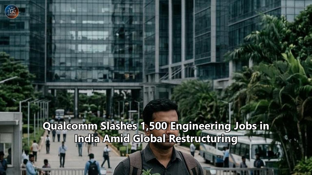
San Diego-based semiconductor powerhouse Qualcomm has initiated a sweeping workforce reduction across its Indian operations, eliminating approximately 1,500 engineering positions across its primary research and development facilities. The exercise, which began at the company’s Bagmane World Technology Centre campus in Bengaluru before expanding to engineering sites in Hyderabad, Chennai, and Noida, accounts for nearly 7.5 percent of Qualcomm’s estimated 20,000-strong Indian workforce. The reductions represent the sharpest staff contraction Qualcomm has ever executed in India, which serves as the multinational's largest engineering footprint outside the United States.
The downsizing stems from a corporate restructuring directive issued in late October by Qualcomm Chief Executive Officer Cristiano Amon. In an internal communication addressed to staff following the company’s annual performance cycle, Amon outlined an initiative to lower global operating costs and realign personnel across business units, putting roughly seven percent of Qualcomm’s 57,000 worldwide headcount at risk.
While Qualcomm framed the initiative internally as a "performance-focused reduction" intended to increase operational accountability, internal accounts, industry disclosures, and separation notices confirm that the job cuts have cut deeply into senior engineering cohorts, including technical leads, principal architects, and domain specialists with unblemished performance appraisals.
===================================================================================
QUALCOMM WORKFORCE RESTRUCTURING: AT A GLANCE
===================================================================================
Global Headcount (FY2026):              ~57,000 employees
Total India Engineering Workforce:      ~18,000 – 20,000 employees
Estimated Positions Cut in India:       ~1,000 – 1,500 engineering roles
Percentage of Domestic Workforce Cut:   5.0% – 7.5%
Key Hubs Affected:                      Bengaluru, Hyderabad, Chennai, Delhi-NCR
Core Divisions Impacted:                RF Front-End, Bluetooth/Wi-Fi Systems,
                                        GNSS, ASIC Design Verification, Modem Firmware
Severance Framework:                    2–3 months base notice + 1 month per year
                                        of service + 12-month medical cover extension
===================================================================================
The retrenchment comes at an ironic juncture. Only months earlier, Qualcomm publicly highlighted its Indian design teams for their pivotal role in executing the successful physical tape-out of its next-generation 2-nanometer (nm) architecture—a critical manufacturing milestone marking the transition of complex electronic designs into physical photomasks for silicon fabrication.
The sudden dismissal of hundreds of engineers responsible for high-complexity design verification, firmware synthesis, and physical layout exposes a structural realignment: Qualcomm is deliberately curtailing investment in mature cellular modem and legacy wireless subsystems to fund an aggressive, capital-intensive pivot toward custom artificial intelligence compute, automotive cockpits, and data-center accelerators.
The Breadth of the Cuts: Who Bears the Brunt?
The operational fallout of the Qualcomm layoffs India reaches across every tier of the company’s domestic engineering hierarchy, dismantling specialized groups that took decades to assemble. Understanding the true impact requires dissecting the profiles of the engineers dismissed, the regional distribution of the cuts, and the structural teams targeted for dissolution.
The Seniority Paradox: High Performers and Domain Leads
Initial expectations within the company suggested the workforce rationalization would follow standard corporate practices: trimming bottom-quartile performers identified during the autumn review cycle. Instead, exit interviews and verified employee disclosures reveal that veteran Application-Specific Integrated Circuit (ASIC) design verification engineers, system-on-chip (SoC) integration specialists, and baseband software architects with tenures spanning seven to twelve years were systematically served termination notices.
Engineers with consistent "exceeds expectations" ratings over consecutive review intervals and professionals actively slated for internal promotions were included in the reductions. The cuts heavily targeted mid-to-senior technical contributors holding base salaries ranging from ₹45 lakh to ₹90 lakh ($53,000 to $107,000 USD) annually, alongside substantial unvested equity packages.
By offloading senior personnel whose compensation compounds through accumulated Restricted Stock Units (RSUs) and seniority premiums, Qualcomm unlocked immediate structural cost reductions that could not be achieved by trimming junior code-maintainers alone.
Regional Footprints: Hyderabad and Bengaluru Bear the Weight
The physical execution of the cuts has reverberated through India's primary hardware clusters:
- Bengaluru (Bagmane World Technology Centre & Bellandur): The Bengaluru campus serves as Qualcomm’s primary hub for core silicon architecture, high-level verification, and advanced computing systems. The site absorbed the initial wave of terminations, with deep reductions across teams working on radio frequency (RF) integrated circuits, board support packages (BSPs), and baseband system verification.
- Hyderabad (Raheja Mindspace & Knowledge City): Housing massive engineering teams dedicated to software engineering, modem firmware, multimedia codecs, and automated testing, Hyderabad-based units saw several specialized design blocks cut, particularly those operating in post-silicon validation and device driver development.
- Chennai and Noida (Delhi-NCR): Operations focused on short-range wireless protocols (Bluetooth, Wi-Fi), analog design, and cellular modem software integration faced targeted consolidations, with select functional clusters reduced by double-digit percentages.
===================================================================================
ESTIMATED REDUCTIONS BY ENGINEERING DOMAIN
===================================================================================
Division / Technology Area         Estimated Impact Level    Core Rationale
-----------------------------------------------------------------------------------
RF Front-End & Analog Design       High                      Handset unit slowdown;
                                                             maturation of 5G RF
Short-Range (Wi-Fi 7 / Bluetooth)  Moderate-to-High          Product line maturity;
                                                             IP block stabilization
Modem Verification & Testbenches   High                      Shifting baseband priorities;
                                                             automation of regression
Automotive & ADAS Systems          Low                       Strategic growth sector;
                                                             ongoing OEM design wins
Oryon CPU Core & Compute NPU       Minimal-to-Zero           High-priority expansion for
                                                             AI PC & server architectures
===================================================================================
The Exit Terms: Structuring the Severance Framework
To cushion the blow and mitigate legal exposure, Qualcomm established a structured separation package for affected personnel. Disclosures indicate that departing employees are receiving two to three months of base pay as standard notice compensation, supplemented by an additional month’s salary for every full year of completed service at the firm.
To expedite execution, the company offered an incentive: an extra month of basic salary for staff who executed exit covenants and liability releases within a 72-hour window.
Medical insurance coverage for employees and their enrolled dependents has been extended for up to twelve months—a crucial buffer given that India’s technology sector is navigating a constrained lateral hiring market. However, the forfeiture of unvested RSUs remains a major financial loss for senior technical personnel, whose long-term incentives constituted up to 40 percent of their realized compensation profiles over rolling multi-year vesting horizons.
What Changes: Silicon Architecture, Product Pivots, and Cost Reallocation
The scale of the Qualcomm layoffs India cannot be divorced from the geopolitical and technological transformations reshaping the global semiconductor supply chain. Qualcomm’s leadership is confronting structural shifts in where semiconductor margin is generated, prompting a reallocation of capital and engineering bandwidth away from legacy segments toward emerging platforms.
                +-----------------------------------------------+
                |   TRADITIONAL REVENUE ENGINE: SMARTPHONES     |
                |   - Maturing 5G Upgrade Cycles                |
                |   - Extended Consumer Replacement Periods     |
                |   - Margin Compression in Handset Chips       |
                +-----------------------+-----------------------+
                                        |
                             RESTRUCTURE CAPITAL
                                        |
                                        v
                +-----------------------------------------------+
                |      AGGRESSIVE CAPITAL REDIRECTION           |
                +-----------------------+-----------------------+
                                        |
         +------------------------------+-------------------------------+
         |                              |                               |
         v                              v                               v
+------------------+         +--------------------+          +--------------------+
|  EDGE AI & NPUs  |         |   AUTOMOTIVE SILICON|          | CUSTOM ORYON CPUS  |
|  Neural compute  |         |   Snapdragon Ride  |          | Windows on ARM,    |
|  for on-device   |         |   chassis & ADAS   |          | enterprise servers |
|  inference models|         |   platforms        |          | and AI PC silicon  |
+------------------+         +--------------------+          +--------------------+
The Smartphone Plateau and Margin Pressures
For nearly two decades, Qualcomm’s core engine has been the mobile handset. The company’s integrated Snapdragon mobile platforms, alongside licensing revenue derived from fundamental Code Division Multiple Access (CDMA) and 5G standard-essential patents, generated reliable cash flow. That dynamic has changed. Global smartphone replacement cycles have lengthened from an average of 24 months to over 38 months in major consumer markets. The incremental utility delivered by year-over-year mobile chip updates has flattened, making it harder to command premium pricing on standard silicon iterations.
Simultaneously, key customer dynamics remain volatile. Despite court-sanctioned licensing compacts and supply agreements that preserve Qualcomm’s modem delivery to Apple through 2026 and 2027, Apple's well-documented multi-billion-dollar effort to commercialize its own in-house 5G and satellite basebands looms as an eventual volume cliff. Qualcomm is moving proactively to shed structural operational overhead before that revenue stream contracts.
The Retreat from Ancillary Wireless Hardware
The targeted elimination of RF front-end, Bluetooth, Wi-Fi, and Global Navigation Satellite System (GNSS) engineering clusters in India reveals an intentional product-line retreat. Rather than sustaining sprawling internal teams dedicated to incrementally refining standalone wireless peripheral chips, Qualcomm is consolidating these intellectual property (IP) blocks into stabilized, automated macro-designs.
When foundational connectivity IP becomes commoditized, maintaining dedicated teams of hundreds of engineers to optimize discrete physical layouts yields diminishing returns. Qualcomm is shifting focus toward high-margin integrated packages where wireless capabilities serve as supporting interfaces rather than the main product value.
Funding the Oryon and Neural Processing Pivot
The capital freed by the workforce reduction is being redirected toward compute and neural processing architectures. Qualcomm’s acquisition of NUVIA for $1.4 billion laid the groundwork for its custom Oryon CPU cores, which now power its Snapdragon X Elite compute platforms. The company is engaged in a high-stakes campaign to capture market share in the personal computing segment, positioning ARM-based architectures as viable, battery-efficient alternatives to traditional x86 processors produced by Intel and AMD.
Scaling this custom CPU and high-performance Neural Processing Unit (NPU) ecosystem requires a different engineering skillset than traditional mobile baseband design. Oryon-class computing demand requires:
- Deep competencies in hardware-software co-design.
- Specialized kernel compilers for machine learning runtimes.
- High-bandwidth unified memory controllers.
- Advanced micro-architecture emulation capable of competing directly with Apple’s M-series silicon and x86 architectures.
Qualcomm’s leadership concluded that its engineering organization carried too much legacy cellular expertise and too little heterogeneous high-performance computing talent. The reduction in India serves as an unsparing workforce rebalancing mechanism.
Short-Term Consequences: Organizational Shockwaves and Talent Market Realities
The immediate aftermath of an engineering reduction of this magnitude generates friction that spreads well beyond human resources departments, disrupting corporate workflows, project roadmaps, and local labor economics.
Institutional Memory Loss and Verification Gaps
Within Qualcomm's Indian engineering facilities, the abrupt departure of veteran engineers creates acute operational vulnerabilities. In modern VLSI (Very Large Scale Integration) semiconductor design, physical layout synthesis and Register-Transfer Level (RTL) code are only part of the development process. A large share of engineering hours is consumed by design verification—building automated UVM (Universal Verification Methodology) testbenches that simulate billions of operating cycles to ensure a complex SoC does not enter a deadlock state.
===================================================================================
VLSI ASIC LIFECYCLE: THE HUMAN DISRUPTION POINT
===================================================================================
Phase                     Primary Activity                 Impact of Sudden Senior Exits
-----------------------------------------------------------------------------------
1. Architecture Spec      Micro-architecture definition    Moderate: Core specs often set
                                                           at HQ (San Diego)
2. RTL Coding             Verilog / SystemVerilog logic    Low-to-Moderate: Core logic
                                                           often modularized
3. Design Verification    UVM Testbenches, regression      CRITICAL VULNERABILITY:
                          suites, corner-case debugging    Loss of institutional insight
                                                           into complex verification suites
4. Physical Design        Synthesis, place-and-route,      Moderate: Highly reliant on
                          clock tree synthesis, timing     standard EDA tool scripts
5. Post-Silicon Val       Bring-up labs, hardware-in-      HIGH VULNERABILITY:
                          the-loop test benches            Loss of lab troubleshooting leads
===================================================================================
When senior verification architects who designed these complex test environments are abruptly separated, their projects lose institutional memory. Junior and mid-level engineers are left to debug opaque, inherited regression scripts with millions of lines of code without access to the architects who built them.
Internal development milestones for derivative chip variants—particularly mid-tier 4nm and 3nm Snapdragon refreshes slated for late-2027 delivery—now face potential schedule slips as remaining personnel scramble to document, decipher, and maintain fragmented validation frameworks.
The Chilling Effect: Survivor Culture and the "January Spectre"
Inside the campuses at Bengaluru and Hyderabad, the restructuring has caused employee morale to plummet. The realization that top-tier performance appraisals provided no defense against termination has dismantled the traditional corporate compact: that technical merit and deep specialized contributions guarantee career stability.
Compounding this psychological strain are reports of a follow-on reduction cycle penciled in for January 2027. The anticipation of a second round of layoffs has paralyzed day-to-day productivity.
Senior engineers who remain with the firm are diverting work hours toward updating resumes, networking with cross-town rivals, and preparing for external technical interviews rather than focusing on chip tape-outs. An engineering organization in self-preservation mode rarely produces the risk-tolerant technical execution required to achieve zero-defect silicon.
Labor Market Absorption: A Transformed Hiring Landscape
The release of up to 1,500 highly compensated, specialized engineers into the domestic market tests the absorptive capacity of India’s hardware ecosystem.
                                  +------------------------------+
                                  | 1,500 DISPLACED QUALCOMM     |
                                  | HARDWARE & SYSTEMS ENGINEERS |
                                  +--------------+---------------+
                                                 |
                         +-----------------------+-----------------------+
                         |                       |                       |
                         v                       v                       v
              +----------------------+ +--------------------+ +----------------------+
              | FABLESS MULTINAT'LS  | | CLOUD HYPERSCALERS | | DOMESTIC ISM STARTUPS|
              | (AMD, Nvidia, Apple, | | (AWS, Google, MSFT | | (Mindgrove, InCore,  |
              | MediaTek, NXP)       | | Silicon Teams)     | | Netrasemi, etc.)     |
              | Status: SELECTIVE    | | Status: EXPANDING  | | Status: CASH-STARVED |
              | Hiring freezes;      | | Aggressively hiring| | Highly interested,   |
              | salary compression   | | custom-silicon engs| | but cannot match pay |
              +----------------------+ +--------------------+ +----------------------+
In previous industry downturns, displaced talent from one blue-chip chipmaker was quickly absorbed by competitors. However, the current semiconductor hiring landscape is characterized by strategic restraint:
- Multinational Semiconductor Rivals: Companies like Intel are managing their own global multi-billion-dollar cost-reduction campaigns and headcount reductions. Texas Instruments, Broadcom, and NXP are maintaining selective hiring models focused on operational replacement rather than footprint expansion.
- The Cloud Hyperscalers: Amazon Web Services (Annapurna Labs), Google, and Microsoft have expanded their custom silicon design teams in Bengaluru and Hyderabad to develop proprietary data-center processors (Graviton, Axion, Azure Maia). These operations represent a primary destination for Qualcomm’s displaced verification and compute architecture leads, though their total intake capacity remains a fraction of the displaced pool.
- The Valuation Reset: Engineers who negotiated 30 to 50 percent pay premiums during the post-pandemic hiring boom of 2021–2022 are facing an altered compensation environment. Rather than securing lateral salary increases, many displaced mid-to-senior engineers are being forced to accept flat compensation packages or concessions in stock grants to secure new roles.
Long-Term Consequences: Reassessing India’s Place in the Global Semiconductor Chain
Beyond the balance sheets and individual career impacts, the downsizing forces an unsparing reassessment of the structural role Indian Global Capability Centers (GCCs) play within multinational technology strategies.
The Fragility of Offshore GCC Seniority
For over twenty years, multinational technology corporations expanded their engineering operations across India, evolving them from low-cost testing extensions into complex development centers responsible for critical products. India hosts more than 1,600 GCCs employing over 1.6 million professionals, with the semiconductor segment historically celebrated as a premier success story.
The cuts at Qualcomm challenge the assumption that Indian technical centers are insulated from global corporate restructuring. Historically, when US-based parent entities faced margin pressure, engineering hubs in emerging markets were protected because of their favorable labor-cost ratios. An experienced ASIC designer in Bengaluru or Hyderabad costs a third of their peer in San Diego or Santa Clara.
However, as Indian centers matured and their operations integrated into end-to-end chip lifecycles, their senior engineering payrolls expanded significantly. A specialized engineering director or principal architect in India, when accounting for base salary, benefits, and international equity grants, now commands compensation packages that represent meaningful operational expenses on a corporate balance sheet.
When multinational leadership demands sweeping, immediate reductions in operating expenditures, high-cost senior engineering positions at offshore facilities become clear targets. The reduction shows that as offshore hubs climb the value-chain ladder, their senior ranks share the same exposure to restructuring as their Western peers.
The Disconnect with the India Semiconductor Mission (ISM)
The retrenchment creates a notable policy contrast with domestic industrial initiatives. The Indian central government, backed by the $10 billion India Semiconductor Mission (ISM), is aggressively subsidizing physical manufacturing infrastructure, committing capital to greenfield fabs and Outsourced Semiconductor Assembly and Test (OSAT) facilities led by the Tata Group, Micron Technology, and CG Power.
===================================================================================
THE INDIAN SEMICONDUCTOR DICHOTOMY
===================================================================================
Government Industrial Policy (ISM)       Multinational Commercial Reality
-----------------------------------------------------------------------------------
- Multi-billion-dollar fab subsidies     - Deep corporate headcount reductions
- Focus on heavy physical capex          - Overhead trimming in fabless engineering
- Sponsoring domestic chip packaging     - Shifting capital to US/Taiwan foundry access
- Subsidizing design startups (DLI)      - Salary compression among elite VLSI talent
===================================================================================
While state and central governments celebrate progress in physical packaging and legacy-node fab construction, the country’s primary competitive advantage—its deep pool of world-class fabless design and validation talent—is exposed to corporate adjustments. The country’s design ecosystem remains predominantly tied to foreign multinational corporations that retain full ownership of intellectual property, design architectures, and workforce allocations.
The Design Linked Incentive (DLI) scheme, intended to nurture domestic fabless startups, remains chronically underfunded relative to the physical fab initiatives. While domestic startups such as InCore Semiconductors, Mindgrove Technologies, and Netrasemi are eager to secure experienced design talent, they lack the capital reserves needed to absorb 1,500 senior engineers accustomed to multinational compensation tiers.
Unless India’s policy ecosystem establishes mechanisms to help domestic startups hire and retain this displaced senior talent, the country risks underutilizing technical capabilities built over decades.
Electronic Design Automation (EDA) and the Generative AI Threat
The structural timing of the layoffs coincides with a technological shift inside silicon engineering environments: the rapid integration of artificial intelligence into Electronic Design Automation (EDA) toolchains.
Major EDA vendors, including Synopsys (with DSO.ai and Synopsys.ai), Cadence Design Systems (with Cerebrus and JedAI), and Siemens EDA, have transitioned from traditional algorithmic layout generation to autonomous, machine-learning-driven optimization. These platforms can optimize:
- Power, Performance, and Area (PPA) balances across complex chip floors.
- Clock-tree synthesis with minimal manual intervention.
- SystemVerilog verification test coverage by autonomously generating corner-case assertions.
Tasks that historically required dozens of verification engineers running manual iterations can increasingly be managed by smaller teams using automated EDA software suites. The workforce reductions in India suggest that Qualcomm is beginning to see the productivity yields of automated design toolchains.
By leaning into AI-accelerated EDA workflows, the company can handle the design implementation of advanced nodes with fewer personnel, reducing its reliance on large physical layout and verification teams.
The Strategic Outlook: What to Watch Next
As Qualcomm executes the remainder of its global restructuring and affected personnel transition into the broader technology ecosystem, several indicators will determine the ultimate impact of this corporate recalibration.
===================================================================================
QUALCOMM STRATEGIC RESTRUCTURING: WATCHLIST
===================================================================================
Milestone / Event            Target Timeline         Strategic Significance
-----------------------------------------------------------------------------------
Q1 FY2027 Earnings Release   Jan / Feb 2027          Will disclose formal severance
                                                     costs and net OpEx reductions
Projected Restructuring      January 2027            Secondary workforce reduction
Wave Two                                             targeting software/systems
Snapdragon X Elite Gen 2     Mid-2027                Validates whether custom CPU
Engineering Tape-Out                                 pivot can maintain schedule
Apple In-House Modem Ramp    Late 2026 - 2027        Tests Qualcomm's vulnerability
                                                     to mobile customer losses
ISM Design Cluster Intake    Through 2027            Measures domestic capacity to
                                                     absorb multinational VLSI exits
===================================================================================
The January 2027 Milestone
The first variable is whether Qualcomm will initiate a secondary round of workforce reductions in early 2027. Reports pointing to follow-on actions suggest the current phase may have targeted immediate hardware cost centers, leaving software maintenance, system validation, and application engineering units subject to review once the current quarter closes.
If a second wave materializes, it will signal that Qualcomm is executing a deeper, permanent contraction of its Indian operational footprint rather than an isolated realignment.
Execution Delivery on the 2nm Roadmap
The technical viability of Qualcomm’s revised strategy will be tested over the coming 12 to 18 months. Having cut hundreds of engineers across its primary design hubs, the company must demonstrate that it can meet strict tape-out and commercial production schedules for its 2nm and 3nm products with TSMC and potentially Samsung Foundry.
Any developmental delays, post-silicon bugs, or validation failures in its high-profile Snapdragon X PC compute silicon or Snapdragon Ride automotive processors will reveal whether the cuts trimmed excess overhead or removed critical technical capacity.
Reconfiguration of India’s Silicon Career Paths
The ongoing Qualcomm layoffs India serve as an inflection point for the domestic engineering community. For a generation of engineering graduates from India’s premier institutions, securing a role within Qualcomm’s cellular modem and baseband units was viewed as an elite career pinnacle.
The retrenchment demonstrates that domain expertise in legacy cellular protocol stacks no longer guarantees long-term career security.
The domestic talent pool faces pressure to adapt, requiring engineers to transition their competencies toward:
- Low-level machine learning compiler development (TVM, MLIR).
- RISC-V architecture optimization.
- Heterogeneous compute fabric integration.
- Hardware-accelerated transformer modeling.
Qualcomm’s retrenchment has shown that the semiconductor industry’s pivot toward artificial intelligence and custom computing architectures will reshape talent structures as swiftly as it updates silicon roadmaps. For India’s hardware engineering ecosystem, the coming years will be defined by how quickly its workforce adapts to this structural realignment.
Reference:
- https://timesofindia.indiatimes.com/business/india-business/qualcomm-layoffs-1500-employees-in-india-amid-restructuring/articleshow/135741996.cms
- https://www.jagranjosh.com/general-knowledge/qualcomm-layoffs-2026-hyderabad-how-many-jobs-are-at-risk-in-india-amid-global-workforce-cuts-1820013766-1
- https://www.business-standard.com/companies/news/qualcomm-starts-india-layoffs-around-1-000-jobs-potentially-at-risk-126111100761_1.html
- https://www.calcalistech.com/ctechnews/article/13if9p1xw
- https://telanganatoday.com/qualcomm-begins-bengaluru-layoffs-hyderabad-may-follow
- https://www.thehindu.com/business/Industry/qualcomm-india-layoffs-over-1000-jobs-at-risk-amid-global-cuts/article71689532.ece
- https://economictimes.indiatimes.com/news/new-updates/qualcomm-layoffs-severance-package-3-months-salary-extra-payout-based-on-years-of-service-one-more-months-pay-for-signing-exit-papers-within-3-days-what-employees-are-being-offered/articleshow/135733726.cms?from=mdr