
At the IEEE International Symposium on Circuits and Systems (ISCAS 2026) in Shanghai, a technical presentation sent a clear signal through the global semiconductor industry. He Tingbo, the head of Huawei’s chip-design division, took the stage to unveil a conceptual departure from traditional silicon scaling. Under intense pressure from international trade sanctions that restrict access to advanced Extreme Ultraviolet (EUV) lithography, the company announced its new "Tau (τ) Scaling Law"—an architectural framework that aims to match the performance of cutting-edge lithography nodes by shifting the focus from physical miniaturization to temporal and spatial routing.
The practical manifestation of this theory is "LogicFolding," a 3D chip architecture debuting in the upcoming Kirin 9050 processor slated for the Mate 90 flagship series this fall. By using advanced electronic design automation (EDA) tools to split a single logical block across two separate, vertically stacked dies connected by an ultra-dense hybrid bonding interface, Huawei claims to have achieved a 53.5% jump in transistor density. The resulting design reaches an effective density of 238 million transistors per square millimeter—on par with TSMC's first-generation 3nm class nodes—using legacy, non-EUV manufacturing equipment.
This announcement is more than a geopolitical workaround; it is a preview of the physical reality facing all chipmakers. For decades, the semiconductor industry relied on Dennard scaling and traditional Moore’s Law to double transistor density every two years simply by shrinking the physical dimensions of the gates. But as the industry approaches the atomic limits of sub-2nm nodes, monolithically shrinking a chip has become economically and physically unsustainable.
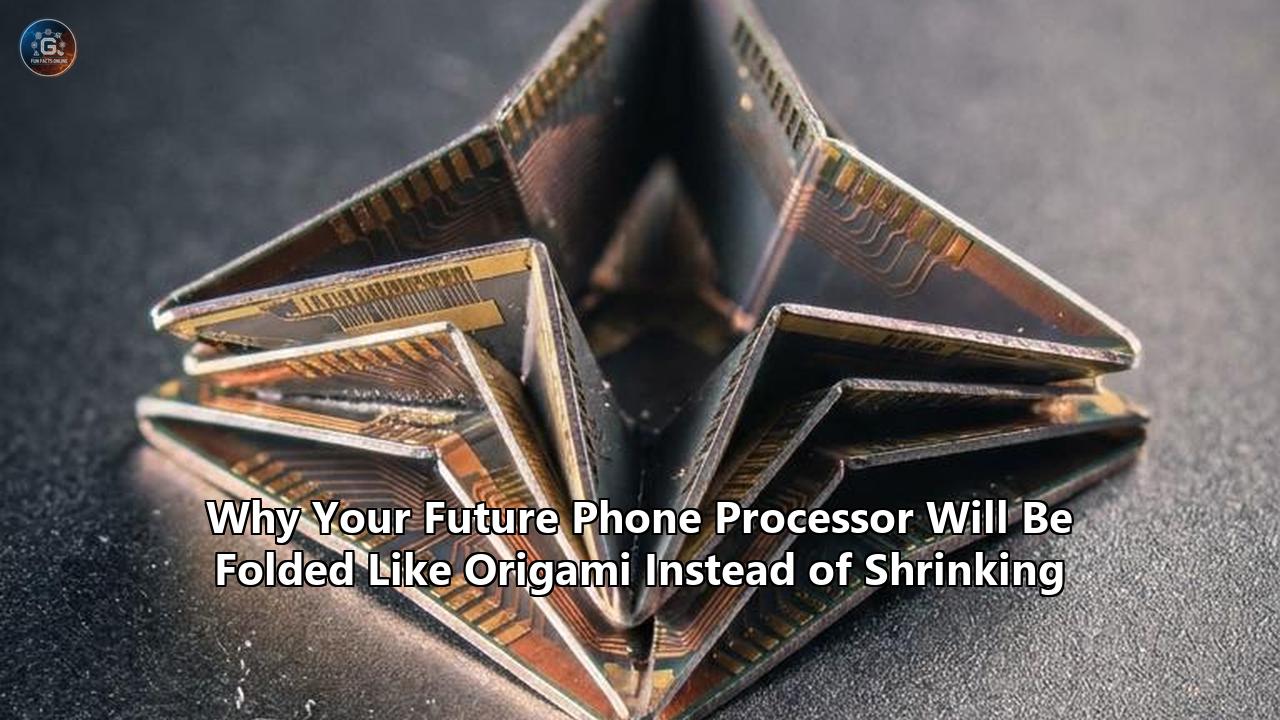
The industry is entering a new era where future smartphone processors will no longer be shrunken down. Instead, they will be folded like origami, utilizing advanced 3D vertical stacking, hybrid bonding, and gate-level partitioning to pack more processing power into the tight volumetric constraints of a mobile handset.
The Physical Wall: Why Monolithic Shrinking Has Stalled
To understand why the industry is turning to 3D vertical stacking, one must first look at the breakdown of classical geometric scaling. For over fifty years, chip design followed a simple rule: shrink the transistor, and it will run faster, consume less power, and become cheaper to manufacture. This virtuous cycle drove the transition from micro-scale integration down to the modern 3nm nodes powering today's flagship mobile devices.
However, as transistor gate lengths approach the single-digit nanometer scale, physical barriers have turned this scaling model on its head.
Monolithic Scaling (2D)               3D Stacking (Origami)
+------------------------+            +-----------+ +-----------+
| Logic  | Cache | I/O   |            |   Logic   | |   Cache   |
+------------------------+            +-----------+ +-----------+
                                            |             |
                                      ===========================  <-- Hybrid Bonding (2μm pitch)
                                            |             |
                                      +-------------------------+
                                      |          Base/IO        |
                                      +-------------------------+
The Quantum Limits of Silicon
At physical dimensions below 5 nanometers, silicon behaves unpredictably. When the gate dielectric layer of a transistor becomes only a few atoms thick, quantum tunneling occurs. Electrons spontaneously jump across the barrier even when the transistor is turned "off," leading to massive static leakage current.
This leakage wastes battery life and generates heat even when a smartphone is sitting idle in a user's pocket. To combat this, foundries transitioned from planar transistors to FinFETs, and more recently, to Gate-All-Around (GAA) architectures like nanosheets. While GAA restoring electrostatic control over the channel, it comes at a steep manufacturing cost and does not solve the underlying interconnect crisis.
The Interconnect Bottleneck and RC Delay
A modern system-on-chip (SoC) contains billions of transistors, but these transistors are useless without the complex web of copper wires (interconnects) that connect them. As transistors shrink, these metal wires must also become thinner and pack closer together.
This introduces two severe parasitic physical phenomena:
- Exponential Resistance Increase: When the width of a copper wire drops below 15 nanometers, the cross-sectional area becomes so small that copper atoms begin to scatter electrons at the wire boundaries. The electrical resistance of the wire increases exponentially.
- Capacitive Coupling: Placing thin metal wires in close proximity creates parasitic capacitance between them.
Together, the increased resistance ($R$) and capacitance ($C$) create a massive "RC delay." In modern future smartphone processors, the time it takes for an electrical signal to travel through the metal wiring on a chip (wire delay) vastly exceeds the time it takes for a transistor to switch (gate delay).
Shrinking a monolithic chip further actually degrades performance because the interconnects become more restrictive.
The Power Density Crisis
Even if lithography could shrink transistors further without increasing wire resistance, thermal dissipation limits prevent these chips from running at high clock speeds.
When transistors are packed closer together in a two-dimensional plane, the power density (Watts per square millimeter) spikes. Smartphone processors must operate within a strict thermal envelope—typically under 5 to 7 Watts under sustained load—because they lack active cooling fans.
If a chip cannot dissipate its heat, it must quickly throttle its clock speeds, rendering its peak performance numbers meaningless during extended gaming or on-device AI workloads.
Bending Time: The Architecture of LogicFolding
Faced with these constraints, semiconductor architects are looking upward. If you cannot pack transistors closer together on a flat plane without ruining the wires and overheating the silicon, you must stack them vertically.
However, vertical stacking is not a monolithic concept. The industry has progressed through several distinct phases of 3D integration, culminating in the gate-level partitioning seen in Huawei’s new LogicFolding scheme.
Comparison of 3D Stacking Paradigms:

1. Advanced Packaging (MCM/CoWoS)
   [ Chiplet A ] --- Interconnect Bridge --- [ Chiplet B ]

2. Block-Level Stacking (AMD 3D V-Cache)
   [ SRAM Cache Die ]
   ================== <-- Hybrid Bonding Interface
   [ Processor Die  ]

3. Gate-Level Folding (Huawei LogicFolding)
   [ Part 1 of Execution Block ]
   ============================= <-- Sub-2μm Hybrid Bonding (Critical Timing Path)
   [ Part 2 of Execution Block ]
Advanced Packaging vs. Block Stacking vs. Logic Folding
To appreciate the architectural leap of LogicFolding, it is helpful to place it alongside existing 3D techniques:
- Advanced Packaging (2.5D): Technologies like TSMC’s Chip-on-Wafer-on-Substrate (CoWoS) place complete, self-contained chips (such as a CPU and High-Bandwidth Memory) side-by-side on a silicon interposer. This is highly effective for massive AI accelerators in data centers but is too bulky and expensive for the ultra-thin chassis of a smartphone.
- Block-Level 3D Stacking (e.g., AMD 3D V-Cache): This involves vertical stacking of independent functional blocks. AMD stacks a separate SRAM cache die directly on top of a Core Complex Die (CCD) using hybrid bonding. The CPU cores and the cache are designed as distinct, complete circuits. If you peel the cache off, the CPU cores can still function with a modified layout. This has been the standard for high-performance computing but has seen limited adoption in mobile due to thermal challenges and the thickness of the stacked assembly.
- Gate-Level Logic Folding: This is the most complex form of 3D integration. Instead of stacking a complete memory block on top of a processor, LogicFolding uses EDA tools to slice a single functional block—such as an ALU (Arithmetic Logic Unit) or an out-of-order execution engine—and distribute its individual logic gates across two distinct silicon layers. A single die contains only half of the logic required to perform a calculation and cannot function independently.
Slicing the Critical Path
In any digital circuit, the maximum clock speed of a processor is dictated by its "critical path"—the longest, slowest sequence of logic gates and interconnect wires that a signal must traverse within a single clock cycle. If a signal cannot complete this journey before the next clock tick, the processor outputs corrupted data.
LogicFolding targets this critical path. Instead of laying out a long critical path horizontally across a single die, EDA tools fold the path vertically.
For example, if an execution block has a critical path consisting of twelve sequential logic gates connected by relatively long horizontal wires, LogicFolding places gates 1 through 6 on the bottom die and gates 7 through 12 directly above them on the top die.
Horizontal Layout (Traditional 2D):
[Gate 1] -> (Long Wire) -> [Gate 2] -> (Long Wire) -> [Gate 3] -> (Long Wire) -> [Gate 4]
Total Path Length: ~150 microns (High resistance, high latency)

Folded Layout (3D LogicFolding):
[Gate 1]                  [Gate 3]
   |                         ^
 (Vertical Bond)           (Vertical Bond)
   v                         |
[Gate 2] -> (Short Wire) -> [Gate 4]
Total Path Length: ~12 microns (Ultra-low resistance, near-instantaneous propagation)
By connecting these two halves with vertical copper interconnects, the physical length of the signal path is reduced from hundreds of micrometers to just a few micrometers. This dramatically trims the parasitic resistance and capacitance (RC load) of the wiring, allowing the signal to propagate much faster.
According to Huawei's presentation, this temporal optimization is what allows a chip built on older, larger transistor geometries to run at the high clock frequencies typically reserved for sub-3nm monolithic designs.
The Engineering Challenge: Ultra-Dense Hybrid Bonding
To make gate-level 3D logic folding work, the interface between the stacked silicon dies must be incredibly dense. Traditional packaging relies on microscopic solder bumps (microbumps) to connect different chips.
However, microbump pitches are limited to around 40 to 25 micrometers. If you tried to connect gate-level logic using microbumps, the sheer size of the contacts would introduce massive parasitic capacitance, completely neutralizing the benefits of folding the circuit.
The enabling technology for true 3D logic folding is copper-to-copper hybrid bonding.
Traditional Microbump Connection (~40μm pitch):
+---------------------------------------+
|              Top Die                  |
+---[Pad]---[Pad]---[Pad]---[Pad]---[Pad]+
      o       o       o       o       o     <-- Solder Bumps
+---[Pad]---[Pad]---[Pad]---[Pad]---[Pad]+
|             Bottom Die                |
+---------------------------------------+

Direct Copper Hybrid Bonding (Sub-2μm pitch):
+---------------------------------------+
|              Top Die                  |
|============[Cu]==[Cu]==[Cu]===========|   <-- Atomic-level Dielectric (SiO2)
|============[Cu]==[Cu]==[Cu]===========|   <-- Cold-welded Copper-to-Copper Joints
|             Bottom Die                |
+---------------------------------------+
How Hybrid Bonding Works
Unlike microbumps, which use physical solder spheres to bridge pads, hybrid bonding joins two silicon wafers directly at the atomic level without any intervening adhesive or solder. The process is highly complex and requires specialized cleanroom environments:
- Deposition and Patterning: The copper contact pads (Vias) and the surrounding dielectric material (usually silicon dioxide or silicon carbonitride) are patterned on the surface of both wafers using high-precision photolithography.
- Chemical Mechanical Planarization (CMP): The surfaces of both wafers are polished to extreme flatness. Any surface roughness greater than a fraction of a nanometer will prevent a successful bond. The copper pads are designed to recess slightly (on the order of a few nanometers) below the level of the dielectric surface during polishing.
- Surface Activation: The polished surfaces are exposed to a plasma (often nitrogen) to activate the dielectric material, making it highly hydrophilic (water-attracting).
- Room-Temperature Bond: The two wafers are precisely aligned and brought into contact at room temperature. The water molecules bound to the activated dielectric surfaces form strong hydrogen bonds, pulling the two wafers together in a molecular-level grip. This initial bond holds the wafers in place with high shear strength.
- Thermal Annealing: The bonded wafer stack is placed in an oven and heated to approximately 300°C to 400°C. This heating causes two critical physical transformations:
The silicon dioxide layers undergo a condensation reaction, forming covalent silicon-oxygen-silicon (Si-O-Si) bonds that permanently fuse the two dielectric surfaces.
Because copper has a higher coefficient of thermal expansion than the surrounding silicon dioxide, the copper pads expand outward, filling the tiny nanometer-scale recesses. The copper atoms migrate across the boundary, recrystallizing into continuous, unified copper-to-copper grain boundaries.
The result is a single, monolithic-like piece of silicon containing two distinct active layers, with no solder, no underfill, and near-zero contact resistance.
The 2-Micron Pitch Milestone
The critical metric for hybrid bonding is the "bond pitch"—the center-to-center distance between adjacent copper connections. First-generation hybrid bonding, such as AMD's 3D V-Cache, used a 9-micrometer pitch. While impressive, a 9µm pitch is far too coarse for gate-level logic routing, restricting its use to memory-on-logic stacking.
To move hybrid bonds into the critical path of a logic block, the pitch must drop below 2 micrometers. At a 2µm pitch, the interconnect density surges to over 250,000 connections per square millimeter. This allows the EDA software to route signal nets vertically between the top and bottom dies with the same flexibility and low latency as standard horizontal metal layers.
Achieving a 2-micron pitch requires sub-micron alignment accuracy during the wafer-bonding process. If the top wafer is misaligned by even 200 nanometers relative to the bottom wafer, the copper pads will fail to align, destroying the yields of the entire run. This requires advanced lithographic alignment systems and rigorous temperature control inside the packaging facility to prevent thermal expansion from drifting the wafers out of alignment.
The Thermal Paradox: Cooling a Stacked Silicon Sandwich
While folding a chip solves the interconnect bottleneck and boosts transistor density, it introduces a severe thermodynamic challenge. Stacking two active, heat-generating silicon dies directly on top of one another creates a thermal sandwich.
Heat Dissipation Pathway in a 3D Stacked Processor:

                  [ Screen / Display ]
                           ^
                           |
            ================================
            [  Backside Power Delivery   ]
            --------------------------------
            [    Top Die (Logic / CPU)   ]  <-- High Heat Generation (Hotspots)
            --------------------------------
            [  Hybrid Bonding Interface  ]  <-- Thermal Barrier
            --------------------------------
            [ Bottom Die (GPU / System)  ]  <-- Trapped Heat Layer
            ================================
                           |
                           v  (Primary Heat Escape Route)
                  [ Vapor Chamber ]
                           |
                           v
              [ Aluminum/Glass Backplate ]
In a traditional monolithic processor, all heat-generating components (like CPU cores and GPUs) are laid out flat against a single piece of silicon. This silicon is in direct contact with a thermal interface material (TIM), which transfers the heat to a copper vapor chamber or graphite sheet, dissipating it through the phone's frame and rear glass.
In a 3D stacked processor:
- Heat Trapping: The top die acts as an insulator for the bottom die. Heat generated in the bottom layer must travel through the hybrid bonding interface, through the top silicon die, and finally into the cooling system.
- Thermal Interface Resistance: Even though hybrid bonding uses direct copper-to-dielectric contact, the interface still presents thermal resistance. This can trap heat in the lower layer, causing its temperature to rise rapidly under load.
- Hotspot Overlap: If the high-power execution units of the top die are placed directly above the high-power graphics processing blocks of the bottom die, a localized thermal hotspot is created. Without careful layout optimization, these localized temperatures can easily exceed 100°C within seconds, triggering aggressive thermal throttling to protect the silicon from physical damage.
Mitigating the Heat: Structural Solutions
To prevent future smartphone processors from becoming thermal liabilities, hardware engineers are deploying a suite of advanced architectural and materials-science solutions:
1. Backside Power Delivery (BSPDN)
Traditionally, both power and signals are routed through a complex web of metal layers on the front side of the silicon wafer. This creates a crowded layout where power delivery wires block signal routing and trap heat.
With Backside Power Delivery—referred to as Intel's "PowerVia" or TSMC's "Super PowerLine"—the power grid is moved entirely to the back of the silicon wafer.
Frontside Power (Traditional):
[ Signal Metal Layers + Power Grid (Intertwined) ]
--------------------------------------------------
[ Active Transistor Layer (GAA/FinFET)           ]
--------------------------------------------------
[ Silicon Substrate (Thick, Passive)             ]

Backside Power (Modern BSPDN):
[ Signal Metal Layers (Unobstructed Routing)     ]
--------------------------------------------------
[ Active Transistor Layer (GAA/FinFET)           ]
--------------------------------------------------
[ Power Grid (Direct delivery from backside)     ]
Moving the thick, highly conductive power delivery lines to the backside provides several thermal and electrical benefits:
- It eliminates the $IR$ (voltage) drop caused by power signals traveling through tiny frontside wires.
- The thick metal lines on the backside act as highly efficient heat spreaders, pulling heat away from the active transistor layer and transferring it directly to the cooling solution.
- It frees up the frontside layers to be optimized purely for signal routing, facilitating tighter logic folding and shorter interconnect paths.
2. Thermal-Aware Co-Design and EDA Layout
To avoid hotspot overlap, chip architects use "thermal-aware design tools." During the floorplanning phase, the EDA software simulates the thermal profile of both dies under various synthetic workloads.
The software ensures that high-power structures on the top die (like the vector units of an AI accelerator) are placed directly over low-power, thermally inactive regions of the bottom die (such as system cache or I/O controllers). This spatial interleaving of hot and cold blocks prevents localized thermal runaway.
3. Silicon-Carbon Battery Technology and Active Cooling
At the device level, phone manufacturers are restructuring the internal layout of handsets to accommodate the thermal profiles of stacked chips.
By transitioning to high-energy-density silicon-carbon batteries, which pack up to 7,000 mAh into ultra-thin profiles, manufacturers can free up critical internal volume. This extra space is being repurposed for massive dual-sided vapor chambers and advanced graphite thermal sheets that wrap around the stacked processor to draw heat from both sides of the motherboard.
The Landscape: TSMC, Samsung, and Intel’s 3D Playbooks
While trade restrictions pushed Huawei to pioneer gate-level LogicFolding out of manufacturing necessity, the rest of the semiconductor industry has been quietly laying the groundwork for its own transition to 3D vertical architectures.
For global giants like TSMC, Samsung, and Intel, the move to 3D is driven by the desire to extend performance scaling as traditional 2nm and 1.4nm nodes become prohibitively expensive to produce on a monolithic basis.
Comparison of Global 3D Packaging Tech:

+-------------------+----------------------------+------------------------+--------------------------+
| Company           | TSMC                       | Samsung                | Intel                    |
+-------------------+----------------------------+------------------------+--------------------------+
| Technology Brand  | SoIC-X (System on Chip)    | SAINT (3D Integration) | Foveros Direct 3D        |
| Current Pitch     | ~9μm (Targeting 3μm)       | ~10μm                  | ~9μm (Targeting sub-5μm) |
| Target Market     | Apple (M5/A20), AMD        | Exynos, Mobile Foundry | Lunar Lake, Mobile SoCs  |
| Primary Stacking  | Face-to-Face / Face-to-Back| Logic + SRAM / DRAM    | Logic + Cache            |
+-------------------+----------------------------+------------------------+--------------------------+
TSMC’s SoIC: The Mobile Pioneer
TSMC’s System on Integrated Chips (SoIC) is the industry's most mature 3D stacking platform. SoIC is split into two primary configurations:
- SoIC-P (Passive): Uses microbumps for cost-effective packaging.
- SoIC-X (Coaxial): Uses direct copper-to-copper hybrid bonding for high-performance applications.
Initially, TSMC's SoIC-X was a low-volume, high-cost technology used primarily by AMD for its Instinct AI accelerators and high-end server processors, where yields originally struggled at around 50%. However, TSMC has rapidly matured the process, bringing SoIC-X yields to over 90%.
TSMC has already integrated SoIC-X support into its high-volume mobile and consumer pipelines. Reports indicate that Apple is planning to adopt TSMC’s SoIC advanced packaging for its next-generation M-series chips and high-end A-series processors.
By stacking high-speed L3 cache or specialized AI accelerator blocks directly on top of the CPU core complex using a fine-pitch hybrid bond, Apple can bypass the physical size limits of a standard monolithic die while keeping latency extremely low.
Furthermore, TSMC’s public roadmap reveals plans to shrink its SoIC hybrid bonding pitch from the current 9 micrometers down to a highly dense 3 micrometers. This brings the foundry giant within striking distance of true gate-level logic stacking for consumer devices.
Intel’s Foveros Direct: The Direct-Bond Challenger
Intel has been a pioneer in 3D stacking since the introduction of its Foveros technology, which used microbumps to stack logic on base dies.
With "Foveros Direct," Intel has transitioned to direct copper-to-copper hybrid bonding, allowing for interconnect pitches below 10 micrometers.
Intel's strategy focuses on building highly modular chiplet architectures. By separating the power-hungry CPU cores, the graphics engine, and the I/O interface into distinct "tiles" fabricated on the most cost-effective process nodes, and then stacking them vertically using Foveros Direct, Intel can optimize each component’s cost and thermal footprint.
While initially targeted at laptops and data centers, Intel's ongoing foundry pivot aims to offer Foveros Direct to mobile chip designers looking to compete with Apple and Qualcomm in the ultra-premium smartphone space.
Samsung’s SAINT: The Memory Integration Play
Samsung Foundry is leveraging its unique position as both a world-class logic foundry and the world’s largest memory manufacturer. Samsung's advanced 3D packaging suite, known as SAINT (Samsung Advanced 3D Integration Technology), is split into three branches:
- SAINT-S (SRAM): Stacks SRAM cache directly on top of the logic die to free up valuable real estate on the primary logic wafer.
- SAINT-D (DRAM): Integrates LPDDR5X or high-bandwidth DRAM directly over the processor, eliminating the lateral wiring paths that limit memory bandwidth in modern smartphones.
- SAINT-L (Logic): Stacks logic on logic, paving the way for advanced multi-layered mobile processors.
Samsung’s strategy is heavily focused on reducing the latency between the processor and memory. In the age of on-device AI, where large language models must constantly fetch weights from memory, the bottleneck is often not the speed of the processor, but the speed of the bus connecting the processor to the DRAM.
By stacking the DRAM directly on top of the processor using SAINT-D, Samsung can provide a massive vertical memory bus with thousands of parallel connections, delivering near-zero latency and a drastic reduction in the power required to move data.
The Economic Equation: Yields, Testing, and the "KGD" Problem
If 3D vertical folding offers such profound performance and power benefits, why hasn't every smartphone chip company fully embraced it? The answer lies in the harsh economics of semiconductor manufacturing. Building a 3D folded processor is vastly more complex and expensive than building a traditional monolithic chip, introducing a new set of economic hurdles.
Monolithic vs. 3D Stacked Yield Math (Simplified):

Monolithic Die (Large):
+-----------------------------------+
|               SoC                 |  <-- Single defect ruins the entire large die.
+-----------------------------------+  Yield: 65%

3D Stacked Dies (Split):
+-------------+      +-------------+
|   Die 1     |      |   Die 2     |  <-- Smaller dies have higher individual yields.
+-------------+      +-------------+  Yields: 90% each
       \                  /
        \                /
       [ Known Good Die Testing ]     <-- Vital step to filter out defects.
                |
       [ Hybrid Bonding Stack ]       <-- Stacking process yield: 95%
                |
       Final Module Yield: 0.90 * 0.90 * 0.95 = 76.9%
The Cost of Bleeding-Edge Wafers
As process nodes advance, the cost of a single processed silicon wafer rises at a steep rate. A single 12-inch wafer fabricated on TSMC’s 3nm node costs approximately $20,000, and 2nm wafers are projected to exceed $25,000.
For a monolithic chip, every square millimeter of silicon must be printed on this expensive leading-edge node, even if certain components do not benefit from the shrink.
SRAM (static random-access memory) and I/O (input/output) controllers do not scale well with geometric shrinks. In fact, SRAM cell sizes have virtually stopped shrinking at the 3nm node, meaning that a larger percentage of a monolithic chip’s expensive real estate is wasted on memory that could easily be fabricated on a cheaper, older node.
3D vertical stacking offers an elegant economic escape hatch:
- Heterogeneous Integration: Chip designers can fabricate the core logic (which benefits from shrinking) on an expensive 3nm or 2nm wafer.
- Older Nodes for Passive Blocks: They can fabricate the SRAM cache, I/O, and power management circuits on a much cheaper, high-yield 5nm or 7nm wafer.
- Bonding Them Together: The two dies are then bonded together using hybrid bonding.
Even with the added cost of the hybrid bonding step, this heterogeneous chiplet approach can be more cost-effective than building a massive, monolithic leading-edge die, because it maximizes the utilization of expensive silicon.
The Known Good Die (KGD) Imperative
However, stacking introduces a critical risk known as the "compounded yield problem."
If you stack two dies together, and one of those dies has a microscopic manufacturing defect, the entire assembled stack must be thrown away. If Die 1 has a yield of 80% and Die 2 has a yield of 80%, stacking them randomly would result in an assembly yield of just 64% ($0.80 \times 0.80$).
To prevent this economic disaster, the industry relies on "Known Good Die" (KGD) testing:
- Prior to bonding, wafers are subjected to rigorous electrical testing using ultra-fine probe cards that make physical contact with the copper pads.
- Only dies that pass these exhaustive testing routines are selected for the stacking process.
- This ensures that defective silicon is discarded before the expensive hybrid bonding step is performed, preserving the yield of the final stacked module.
Implementing KGD testing at a 2-micron pitch is incredibly difficult. Traditional mechanical probe cards cannot easily target pads that are only 1 to 2 micrometers wide without damaging them.
The industry has had to develop optical and contactless testing methodologies—utilizing localized electron beams or RF induction—to verify the integrity of the logic circuits before they are aligned and fused together.
What This Means for Consumers: The Smartphone of 2030
The shift from monolithic shrinking to vertical origami is not just an academic milestone for semiconductor engineers; it will fundamentally reshape what a smartphone is capable of doing. As future smartphone processors transition to 3D vertical architectures over the coming years, users will experience tangible changes in performance, battery life, and device design.
Impact of 3D Stacked Processors on Smartphone Design:

Traditional 2D Processor Layout           Modern 3D Folded Processor Layout
+---------------------------------+       +---------------------------------+
|             Battery             |       |             Battery             |
|                                 |       |        (Expanded Capacity)      |
|                                 |       |                                 |
+---------------------------------+       +---------------------------------+
|   Motherboard (Large, flat)     |       |   Motherboard (Tiny, dense)     |
|  [ SoC ]  [ RAM ]  [ PMIC ]     |       |  [ 3D Stacked SoC + DRAM ]      |
+---------------------------------+       +---------------------------------+
|  Thicker Bezels / Bulky Chassis |       |  Ultra-thin Foldable Chassis    |
+---------------------------------+       +---------------------------------+
1. The Death of Thermal Throttling
We have all experienced our phones becoming uncomfortably warm and noticeably slower during an intense gaming session or while recording 4K video. This is the result of thermal throttling—the processor stepping down its performance to prevent overheating.
With 3D logic folding and the integration of Backside Power Delivery, processors will run cooler at sustained workloads.
By bypassing the resistive copper wiring that generates passive heat, and using advanced thermal co-design to spread hotspots across multiple layers, future smartphone processors will be able to maintain their peak clock speeds for hours without performance degradation.
This sustained performance is crucial for mobile gaming and sustained on-device AI workloads.
2. On-Device AI: The Power of Localized Intelligence
The current wave of generative AI tools (like DeepSeek, ChatGPT, and localized LLMs) relies heavily on cloud computing, which introduces latency and raises privacy concerns. Running these models locally on a smartphone requires immense computational power and massive memory bandwidth.
3D stacked processors are uniquely positioned to solve this. By stacking a high-performance Neural Processing Unit (NPU) directly under or over high-density LPDDR5X DRAM or stacked SRAM cache, the bandwidth bottleneck is eliminated.
An on-device AI will be able to access the millions of parameters of a localized LLM with zero bus delay and at a fraction of the power consumption. This will enable real-time, low-latency voice translation, local video rendering, and deep context-aware personal assistants that operate entirely offline, preserving both privacy and battery life.
3. Ultra-Thin and Foldable Form Factors
As smartphones move toward multi-hinge foldables and ultra-thin form factors—such as Huawei's tri-fold Mate XT—the internal space inside the chassis is at an absolute premium. Every cubic millimeter occupied by the motherboard is a cubic millimeter that cannot be used for the battery.
Volumetric Efficiency Comparison:
Traditional 2D SoC + Discrete RAM + Discrete PMIC:
Form Factor: 15mm x 15mm x 1.2mm = 270 cubic millimeters of occupied space.

3D Folded SoC (Stacked Logic + Stacked Cache + Stacked PMIC):
Form Factor: 8mm x 8mm x 1.6mm = 102.4 cubic millimeters of occupied space.
Result: Over 60% reduction in occupied motherboard footprint, allowing for a 15% larger battery.
By compressing the physical footprint of the processor, RAM, and power management units into a single vertically stacked 3D module, motherboard dimensions can be slashed.
This freed-up volume allows phone manufacturers to pack larger, high-density silicon-carbon batteries into incredibly thin designs, ensuring that even a tri-folding phone with a massive screen can easily last through a full day of heavy use.
Looking Ahead: The Next Milestone in 3D Silicon
The semiconductor industry is undergoing its most significant structural shift since the invention of the integrated circuit. The announcement of Huawei's Tau Scaling Law and LogicFolding architecture at ISCAS 2026, alongside TSMC’s aggressive SoIC roadmap and Intel’s Foveros developments, marks the end of the two-dimensional scaling era.
For decades, we judged a chip's progress by a single, physical dimension—the nanometer. In the very near future, that metric will become largely irrelevant.
Instead, the performance of future smartphone processors will be defined by their spatial architecture: how many layers they possess, the density of their hybrid bonding interfaces, and the sophistication of the EDA algorithms that fold their logical paths across the vertical plane.
As the first commercial devices powered by these folded architectures hit the market later this year, the industry will watch closely. The success of these initial designs will determine how quickly the rest of the consumer tech world transitions to 3D silicon origami.
One thing is certain: the path forward for mobile processing is no longer about shrinking the canvas. It is about folding the paper.
Reference:
- https://seekingalpha.com/news/4596579-huawei-unveils-advanced-chip-design-breakthrough-amid-us-curbs
- https://richardsgadgets.substack.com/p/huaweis-logicfolding-chip-tech-aims
- https://pandaily.com/huawei-kirin-9050-surpasses-apple-a18-may2026
- https://www.reddit.com/r/technology/comments/1to53t6/huawei_presents_the_tau_%CF%84_scaling_law_enabling/
- https://www.revibyte.blog/posts/latest-smartphone-releases-2026/
- https://www.tweaktown.com/news/99217/apple-expected-to-use-tsmcs-2nm-process-soic-packaging-tech-in-2h-2025/index.html
- https://www.tomshardware.com/tech-industry/semiconductors/tsmc-soic-3d-stacking-roadmap-outlines-path-from-6-micron-pitches-today-to-4-5-micron-in-2029-fujitsus-monaka-cpu-to-benefit-from-face-to-face-chiplet-stacking
- https://semiengineering.com/next-gen-3d-chip-packaging-race-begins/
- https://www.wevolver.com/article/hybrid-bonding-enabling-high-density-3d-integration-for-next-generation-electronics
- https://3dfabric.tsmc.com/english/dedicatedFoundry/technology/SoIC.htm
- https://www.youtube.com/watch?v=HGYBnOk5RSk