
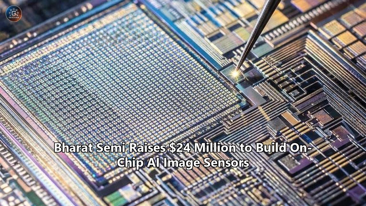
New Delhi-based semiconductor designer Bharat Semi has closed a $24 million all-equity seed funding round to accelerate the development of custom image sensors that integrate artificial intelligence processing directly onto silicon dies. The financing, completed in mid-November 2026, represents one of the largest seed commitments ever made to an Indian fabless semiconductor startup.
The round was led jointly by Info Edge Group, South Park Commons, and Indus Bridge Ventures, with participation from Indian consumer hardware firm Micromax, Valour Capital, New York-based Gaingels, and angel investors Mukul Agarwal and Karthik Sundar Iyer.
The pre-revenue company is racing to bring programmable on-chip AI image sensors into commercial production by 2027. Unlike conventional digital imaging pipelines that offload raw pixel streams across printed circuit boards to standalone image signal processors (ISPs) and host processors, Bharat Semi is engineering a single-die stack capable of photon capture, optical correction, and neural network inference simultaneously.
Early commercial validation has already surfaced. Bharat Semi confirmed it has secured early design wins with San Diego-based defense contractor General Atomics Aeronautical Systems—the prime manufacturer of the MQ-9 Reaper and Predator drone platforms—and Indian outsourced semiconductor assembly and test (OSAT) firm Kaynes Semicon.
The fresh injection of capital is structured to finance roughly 30 months of operational runway. The funds will support silicon prototyping, toolchain maturation, and an international engineering push across Santa Clara, California, and select European design centers.
Traditional Vision System (Multi-Chip)
┌────────────────┐      MIPI CSI-2     ┌────────────┐      High-Speed Bus     ┌────────────────┐
│  Image Sensor  │ ──────────────────> │  Ext. ISP  │ ──────────────────────> │ Host SoC / NPU │
│  (Photon Conv) │  [1.5–3.0W, Latency]│ (Filtering)│   [DRAM Read/Write Tax] │ (Deep Learning)│
└────────────────┘                     └────────────┘                         └────────────────┘

Bharat Semi Integrated Architecture (Heterogeneous 3D Stack)
┌──────────────────────────────────────────────────────────────────────────────────────────────┐
│ Top Die: BSI Pinned Photodiode Array (Engineered for High Dynamic Range & Quantum Efficiency)│
├──────────────────────────────────────────────────────────────────────────────────────────────┤
│ Interconnect: Direct Cu-Cu Hybrid Bonding / Through-Silicon Vias (Sub-picojoule/bit)         │
├──────────────────────────────────────────────────────────────────────────────────────────────┤
│ Bottom Die: Column-Parallel ADCs + Hardened ISP + Programmable NPU (Inference on Focal Plane)│
└──────────────────────────────────────────────────────────────────────────────────────────────┘
                                               │
                                               ▼
                             Metadata Output (<100 Bytes/Frame)
                             Target Actions, Bounding Boxes, Telemetry
The Silicon Bottleneck: The Energy Cost of Moving Raw Pixels
The engineering motivation behind integrating machine intelligence into the focal plane addresses a physical limitation of standard embedded vision systems: data movement consumes far more power than computation.
In a conventional camera setup—whether installed on an industrial automated guided vehicle, a domestic appliance, or a long-endurance unmanned aerial vehicle (UAV)—the signal path is divided across three distinct physical packages:
- A CMOS image sensor (CIS) captures incoming photons across a photodiode array and converts analog charges into raw digital values.
- A dedicated Image Signal Processor (ISP) takes those raw pixels over a multi-lane high-speed serial bus (typically MIPI CSI-2) to handle demosaicing, noise reduction, white balance, and lens shading correction.
- A central System-on-Chip (SoC) or discrete Neural Processing Unit (NPU) pulls that processed video stream into dynamic random-access memory (DRAM) and runs computer vision algorithms across CPU cores, vector engines, or tensor accelerators.
Moving uncompressed video across these component interfaces creates a severe energy penalty. A standard 4K image stream running at 60 frames per second generates upwards of 12 gigabits per second of raw data. Transporting that volume across PCB copper traces, serializer/deserializer (SerDes) circuits, and external LPDDR interfaces dissipates between 1.5 and 3.0 watts of continuous power before deep learning inference even begins.
For battery-limited platforms, thermal dissipation and power draw limit what systems can deploy. A loitering reconnaissance drone or a battery-powered security perimeter node cannot support desktop-class compute modules simply to confirm whether a human form or vehicle has crossed into view.
"Moving data between components creates latency, power, and cost burdens, particularly for drones, robots, and other devices with tight power budgets," Bharat Semi explained in its technical product briefing.
By collapsing these distinct stages into on-chip AI image sensors, visual data is processed where it is captured. The device discards irrelevant pixel noise directly on the silicon stack. Instead of streaming continuous gigabytes of high-bandwidth video over high-speed buses to an external processor, the chip extracts spatial gradients, runs convolutional or transformer-based tensor operations, and outputs compact semantic metadata—such as bounding boxes, class probabilities, or motion vectors.
"Our aim here is to move from sensors to sense-making solutions," co-founder and chief executive officer Vrinda Kapoor explained.
Data Pipeline Transformation:
Conventional:  4K60 Raw Frame (~1.5 GB/s) ──> Full ISP Pipeline ──> DDR Memory Bus ──> NPU Execution
On-Chip Stack: Photodiode Absorption     ──> Sub-surface Tensor Compute ──> Structured Telemetry (<1 KB/s)
Anatomy of the Stack: Interconnects and Thermal Physics
Combining high-sensitivity optical sensing with dense digital computing requires overcoming a fundamental incompatibility in silicon manufacturing: the process nodes that produce good photodiodes do not produce fast, efficient logic gates.
Image sensor pixels require specialized, high-voltage analog processes (often 65-nanometer to 180-nanometer lithography) to maximize fill factors, minimize dark current, and prevent electron leakage between neighboring wells. Deep learning accelerators, conversely, rely on sub-28-nanometer planar or advanced FinFET nodes to maximize clock frequencies, pack SRAM density, and minimize switching energy per multiply-accumulate (MAC) operation.
Attempting to manufacture both on a single planar silicon substrate forces severe compromises. The analog pixels end up noisy and cramped, while the digital logic becomes slow and power-hungry.
+--------------------------------------------------------------------+
| 1. Optical Tier (Analog Optimized Fab: 65nm–180nm)                |
|    - Microlens & Color/Wavelength Filters                          |
|    - Backside-Illuminated (BSI) Pinned Photodiodes                 |
|    - Integrated Deep Trench Isolation (DTI)                        |
+--------------------------------------------------------------------+
| 2. Bonding Interface (Direct Cu-Cu Hybrid Bonding)                 |
|    - Sub-micron pitch interconnect grid                            |
|    - Ultra-dense Through-Silicon Vias (TSVs)                       |
+--------------------------------------------------------------------+
| 3. Digital Logic Tier (Standard Logic Fab: 22nm/28nm FinFET)       |
|    - Column-Parallel Single-Slope or SAR ADCs                      |
|    - Hardwired Image Preprocessing Block (Cropping/Scaling)        |
|    - Low-Power NPU Array (Integer Quantized MAC Units)             |
|    - Local On-Chip SRAM Cache (Weight & Feature Storage)           |
+--------------------------------------------------------------------+
To resolve this dichotomy, Bharat Semi's architecture uses heterogeneous three-dimensional (3D) wafer-level stacking, an advanced packaging technique pioneered by high-tier consumer sensor manufacturers:
- The Top Optical Tier: Fabricated on an analog-optimized CMOS image sensor line, this layer contains a Backside-Illuminated (BSI) pinned photodiode array. Placing the wiring grid underneath the photodiode layer clears an unobstructed path for incoming photons, maximizing quantum efficiency and angular light acceptance. Deep Trench Isolation (DTI) etching surrounds each pixel, preventing optical and electrical crosstalk across adjacent channels.
- The Bottom Logic Tier: Manufactured on a standard low-power logic node (such as 22nm or 28nm), this wafer contains column-parallel analog-to-digital converters (ADCs), a streamlined digital ISP, and a programmable tensor processor paired with tightly coupled local SRAM.
- The Hybrid Bonding Layer: Rather than using micro-bumps or wire bonds, the two wafers are bonded face-to-face via direct copper-to-copper (Cu-Cu) hybrid bonding, combined with oxide-to-oxide fusion. This technique provides vertical connection pitches below two micrometers, creating a massive, highly parallel interface between the pixel array and the underlying processing units.
Thermal Dissipation and Dark Current Challenges
While 3D stacking solves the interconnect bandwidth problem, it introduces a severe thermal physics challenge: thermal noise.
CMOS photodiodes are vulnerable to temperature increases. As silicon heats up, thermal agitation generates spontaneous electron-hole pairs within the depletion region of the photodiode. This produces dark current—a spurious electrical signal that registers as noise in the absence of light. In standard sensors, dark current roughly doubles for every 6 to 8 degrees Celsius rise in junction temperature, severely degrading dynamic range and signal-to-noise ratios in low-light environments.
Digital neural processing units generate significant thermal energy. When an on-chip NPU executes billions of operations per second running quantized weights, it produces localized hotspots. If that heat bleeds vertically through the hybrid bonding layer into the top photodiode tier, the sensor's optical performance degrades rapidly, blinding the camera with noise patterns.
Engineering around this thermal coupling is central to Bharat Semi's design methodology. Insiders close to the engineering team indicate that the startup is attacking the problem through three complementary techniques:
- Aggressive Integer Quantization: The integrated NPU executes ultra-low-precision arithmetic (INT8, INT4, and ternary networks). Restricting inference to lower bit-widths reduces the switching capacitance of the multiply-accumulate array by more than 70% compared to standard floating-point engines, keeping logic power draw in the milliwatt regime.
- Selective ROI (Region-of-Interest) Gating: The logic die does not run deep neural networks across every pixel in every frame. Instead, ultra-low-power, analog-domain threshold comparators on the upper tier flag dynamic changes in the scene. Only sub-regions displaying meaningful motion or contrast shifts trigger clock generation and execution within the underlying logic blocks, leaving the rest of the digital array in deep sleep.
- Engineered Thermal Isolation Layers: The dielectric bonding materials between the logic substrate and the active photodiode layer incorporate heat-spreading barrier layers designed to channel heat laterally toward the chip package perimeter, rather than allowing it to rise into the optical substrate.
Deconstructing the "70% Cost Reduction"
In announcing the seed round, Bharat Semi claimed its integrated architecture could slash total system bills of materials (BOM) by at least 70% compared to traditional multi-chip implementations.
Independent hardware engineers usually treat claims of that magnitude with skepticism. Custom 3D-stacked silicon is notoriously expensive to tape out, and wafer-to-wafer bonding yields can fall quickly if particle defects contaminate the cleanroom interface.
To determine how the company projects a 70% savings, one must look beyond the cost of the silicon die itself and analyze the broader electronics manufacturing workflow:
| Component Category | Traditional Multi-Chip Vision Pipeline | Bharat Semi Integrated Architecture | Net System Impact |
|---|---|---|---|
| Silicon Packages | • CMOS Image Sensor ($5–$15) • External Hardware ISP ($3–$8) • Host Edge SoC / NPU ($25–$60) | • Single 3D-stacked on-chip AI image sensor ($15–$25) | Eliminates two packaged ICs; saves packaging and test margins across multiple vendors. |
| Memory Subsystem | • External LPDDR4/5 SDRAM chip ($8–$18) • Dedicated Flash for SoC OS boot ($3–$6) | • On-die SRAM for weight caching; minimal external non-volatile memory | Eliminates high-speed DRAM bus traces and commodity external DRAM chips entirely. |
| Power Delivery | • Complex PMIC with 6–10 independent voltage rails ($4–$8) • Bulky discrete inductors/capacitors | • Simplified low-dropout regulators (LDOs) and 2–3 core supply rails ($1.50–$2.50) | Reduces board footprint, reduces passive component count, and simplifies power sequencing. |
| PCB Layout & Routing | • High-density interconnect (HDI) PCB • 8–12 layers required for impedance-matched DDR/MIPI buses | • Standard 4–6 layer low-cost PCB • Low-speed metadata output bus (SPI, I2C, UART, or basic Ethernet) | Drastically reduces PCB fabrication costs and trace layout design complexity. |
| Optics & Enclosure | • Large housing required to sink 5–15W of cumulative heat from SoC, ISP, and DRAM | • Compact, sealed enclosure supported by milliwatt-scale thermal profile | Enables smaller, lighter devices; critical for micro-UAVs and space-constrained robotics. |
A standard edge AI vision board requires a high-density, multi-layer printed circuit board (PCB) with tight trace geometries to route high-speed differential signal lanes between the sensor, the ISP, and the processor, plus clean power distribution for LPDDR memory buses. The engineering labor, testing overhead, and passive component counts associated with high-speed memory routing add substantial cost to industrial cameras.
By executing the entire machine perception loop inside a single component, the customer's carrier board transforms into a basic carrier. The sensor requires only low-speed interfaces—such as an SPI, UART, or basic controller area network (CAN) bus—to transmit inferences to the host system controller.
While the unit cost of a 3D-stacked sensor die exceeds that of a simple commodity photodiode, it undercuts the total cost of purchasing, placing, routing, and cooling three separate advanced chips.
The Fowler Factor: Industry Pedigree in New Delhi
Startups in emerging semiconductor hubs often face a credibility hurdle: hardware design is unforgiving, and the path from architectural simulation to high-yielding silicon is littered with failed tape-outs.
Bharat Semi offset that operational risk in May 2025 by recruiting Dr. Boyd Fowler as its Chief Technology Officer.
Fowler's appointment brought institutional engineering knowledge to the company's Santa Clara and New Delhi offices. Holding a master’s and doctorate in electrical engineering from Stanford University, Fowler has spent more than three decades at the forefront of digital image sensing.
Early in his career, Fowler co-founded Pixel Devices, an imaging venture acquired by Agilent Technologies. While at Pixel Devices, he led the collaborative engineering push with Taiwan Semiconductor Manufacturing Co. (TSMC) that realized the first commercially viable four-transistor (4T) pinned photodiode pixels. That advance reduced readout noise, eliminated image lag, and laid the foundation for the CMOS image sensors used across billions of mobile devices and machine vision systems today.
Boyd Fowler: Career Trajectory & Architectural Influence
┌───────────────────────────┐
│ Stanford University (PhD) │ ──> Foundational research in CMOS noise characteristics & image sensors
└─────────────┬─────────────┘
              ▼
┌───────────────────────────┐
│ Pixel Devices (Co-Founder)│ ──> Developed the first commercial 4T pinned photodiode pixels with TSMC
└─────────────┬─────────────┘
              ▼
┌───────────────────────────┐
│ Fairchild / BAE Systems   │ ──> CTO: Scientific CMOS (sCMOS), high-performance defense imagers
└─────────────┬─────────────┘
              ▼
┌───────────────────────────┐
│ OMNIVISION Technologies   │ ──> CTO: Ultra-compact mobile CIS, automotive & 3D stacked wafer scaling
└─────────────┬─────────────┘
              ▼
┌───────────────────────────┐
│ Bharat Semi (CTO, 2025– ) │ ──> Directing 3D-stacked on-chip AI image sensors for Physical AI workloads
└───────────────────────────┘
Fowler subsequently served as Chief Technology Officer at Fairchild Imaging, where he helped pioneer scientific CMOS (sCMOS) sensors for aerospace and surveillance applications before the business was absorbed by defense major BAE Systems. He later assumed the role of CTO at OmniVision Technologies, guiding the company through its transition into stacked wafer architectures, automotive imaging systems, and high-volume consumer sensing.
Fowler’s presence at Bharat Semi indicates that the startup's architectural approach is grounded in proven production methodology. A technologist with direct experience qualifying pixel architectures on TSMC's manufacturing lines gives the company internal access to the design rules, noise modeling algorithms, and foundry interfacing techniques required to take complex mixed-signal silicon into mass production.
"Before joining Bharat Semi, Boyd defined long-term technology visions and ran complex engineering organizations where discipline, scale, and execution are critical," the company noted when announcing his appointment.
The Geopolitical Chessboard: Defense Alliances and China De-risking
Bharat Semi’s rapid rise from an academic research project into an internationally backed startup is tied to global semiconductor geopolitics and supply chain diversification.
The enterprise began in 2019 at the Indian Institute of Technology (IIT) Delhi's image sensor laboratory, where Vrinda Kapoor (a computational biologist by training), Vinayak Dalmia (a former McKinsey consultant and private equity investor), and Professor Mukul Sarkar conceived an imaging spin-off called 3rdiTech. The team focused on low-light CMOS imaging sensors designed to address a critical vulnerability in India's national security apparatus: the country had no domestic source for electro-optical sensors, forcing its military to import roughly $1 billion worth of thermal, night-vision, and guided-seeker components annually.
After developing low-light sensors that earned the Indian Army Design Bureau’s Award of Excellence and winning contracts under the Indian Ministry of Defence’s Innovations for Defence Excellence (iDEX) framework, the founders expanded their ambitions. In late 2021, they formed Bharat Semi as a specialized vehicle to scale these imaging architectures into global commercial and dual-use markets.
Ecosystem Lineage: From Laboratory to Transatlantic Defense
┌────────────────────────────────────────────────────────────────────────┐
│ IIT Delhi Image Sensor Lab (Prof. Mukul Sarkar, Kapoor, Dalmia - 2019)  │
└───────────────────────────────────┬────────────────────────────────────┘
                                    ▼
┌────────────────────────────────────────────────────────────────────────┐
│ 3rdiTech: Indian Defense R&D (iDEX, Army Design Bureau Award)          │
└───────────────────┬────────────────────────────────┬───────────────────┘
                    │                                │
                    ▼                                ▼
┌───────────────────────────────────────┐ ┌──────────────────────────────┐
│ Strategic Defense Track:              │ │ Commercial & Edge Track:     │
│ "Shakti" Fab Project (Jewar, UP)      │ │ Bharat Semi (New Delhi/US)   │
│ - US Space Force Partnership          │ │ - $24M Seed (Nov 2026)       │
│ - Compound Silicon: GaN, SiC, InGaAs  │ │ - Fabless Business Model     │
│ - Integrated Device Manufacturer (IDM)│ │ - General Atomics Win        │
└───────────────────────────────────────┘ └──────────────────────────────┘
The startup operates at the intersection of two overlapping strategic efforts:
1. The Fabless Commercial Venture (Bharat Semi)
The $24 million seed financing reported in November 2026 applies exclusively to Bharat Semi’s fabless sensor company. This entity outsources fabrication to external foundries, focusing internal capital on custom sensor layout, digital logic design, embedded firmware, and neural-compiler software.
2. The Strategic "Shakti" Compound Semiconductor Fab
In September 2024, the Indian and United States governments issued a joint statement announcing the establishment of "Shakti"—a planned national security semiconductor fabrication facility in Jewar, Uttar Pradesh.
Formed through a partnership among Bharat Semi, 3rdiTech, and the United States Space Force, and backed by capital subsidies from the India Semiconductor Mission (ISM), the Shakti fab is being engineered as a dedicated multi-material facility. It is designed to manufacture compound semiconductors—including Gallium Nitride (GaN), Silicon Carbide (SiC), and Indium Gallium Arsenide (InGaAs) infrared sensors—for military radar, high-voltage power arrays, and electronic warfare systems.
Kapoor has explicitly clarified that the two operational tracks are financially and structurally distinct. None of the $24 million seed capital will be used to fund the construction or tooling of the Shakti fab.
"Bharat Semi intends to remain fabless in its image-sensor business, outsourcing chip manufacturing while focusing on semiconductor design and software," Kapoor stated. "The fab initiative remains in development while we work to identify domestic partners that would build and operate the facility".
De-risking Western Defense Supply Chains
Despite these corporate divisions, Bharat Semi's design win with General Atomics highlights a commercial driver behind both ventures: Western defense contractors are systematically removing Chinese components from their hardware supply chains.
The global market for visual sensors has historically concentrated in Asia. While Sony dominates high-end consumer imaging from Japan, and Samsung retains major capacity in South Korea, the cost-effective CMOS sensors used in industrial surveillance, consumer hardware, and small drones are predominantly manufactured by entities tied to Chinese capital—such as OmniVision (acquired by Will Semiconductor in 2019) and domestic suppliers like GalaxyCore.
Global Machine Vision Landscape & Geopolitical Cleavages
┌─────────────────────────────────┐   ┌─────────────────────────────────┐
│     Incumbent Asian Giants      │   │   U.S.-India Strategic Axis     │
├─────────────────────────────────┤   ├─────────────────────────────────┤
│ • Sony (Dominant in Consumer)   │   │ • Bharat Semi Design Engine     │
│ • Samsung (ISOCELL Mobile)      │   │ • General Atomics Integration   │
│ • Will Semi / OmniVision (China)│   │ • US Space Force Dual-Use Ties  │
│ • GalaxyCore / Smartsens (China)│   │ • Kaynes Semicon Packaging (IN) │
└────────────────┬────────────────┘   └────────────────┬────────────────┘
                 │                                     │
                 ▼                                     ▼
   Exposed to National Defense           Meets NDAA / iCET Security
    Export Bans & Trade Tariffs            Framework Requirements
For Western aerospace platforms, these dependencies pose operational and regulatory risks. Under United States National Defense Authorization Act (NDAA) guidelines, defense suppliers are barred from incorporating imaging hardware, microelectronics, or telecommunications chips produced by specific Chinese technology firms into military systems.
General Atomics' engagement with Bharat Semi reflects a deliberate move to foster an alternative, non-Chinese ecosystem for intelligent sensors. Supported by the U.S.–India Initiative on Critical and Emerging Technologies (iCET), the partnership pairs American defense aerospace systems with an Indo-U.S. fabless designer capable of building hardware that complies with Western supply chain security mandates.
Designing for "Physical AI": The Machine Perception Shift
While defense procurement provides early, high-margin revenue, Bharat Semi’s broader commercial strategy targets what technology markets call "Physical AI"—autonomous systems that must interact safely with physical environments.
"In the near future, growth in the sensor market will be driven by capturing data for machines," co-founder Vinayak Dalmia said following the funding announcement. "This data may never be seen by humans, but it will drive AI at the edge. This requires a different type of system, where sensing, processing, and software are designed together. AI algorithms and hardware have improved enough to make Physical AI a reality, and we intend to define this category".
Traditional Camera Pipeline (Human-Centric Target)
[ Photons ] ──> [ Raw Pixels ] ──> [ ISP: Demosaic, Denoise, Color Balance ] ──> [ Display: Screen ]
* Goal: Photorealistic representation tailored to human eye perception curves.

Machine Vision Pipeline (Tensor-Centric Target)
[ Photons ] ──> [ Focal-Plane Processing: Spatial Derivatives, Temporal Contrast ] ──> [ Direct Tensors ]
* Goal: Feature extraction, edge telemetry, occupancy classification, and tracking vectors.
Engineering sensors for machines rather than humans alters the design priorities of the silicon:
- Eliminating the Color Penalty: Human vision requires accurate color reproduction, requiring sensors to overlay complex Bayer color filter arrays that absorb up to 60% of incoming light. Machine learning models rarely need full RGB color fidelity to detect obstacles, track objects, or recognize motion paths. Designing sensors that capture luminance or infrared spectrums across specialized pixel bands yields higher sensitivity, higher frame rates, and superior low-light performance.
- Skipping Photographic Corrections: Traditional ISPs spend extensive clock cycles and electrical power demosaicing color patterns, adjusting dynamic range curves, and sharpening edges for human visual aesthetics. A deep learning classifier processes matrix numbers directly. Bypassing human-centric image rendering pipelines cuts latency down to sub-millisecond ranges.
- Pixel-Level Privacy-by-Design: In consumer settings—such as smart home air conditioners that sense room occupancy or factory monitoring systems—streaming video feeds across external networks raises severe data privacy concerns. Bharat Semi's architecture resolves this at the hardware level: raw video frames never leave the sensor substrate. The silicon extracts spatial tokens and immediately overwrites the buffer, outputting numerical vectors indicating presence or activity without generating an interceptable video feed.
With investment institutions such as Morgan Stanley projecting the deployment of approximately one billion humanoid robots globally by 2050, the demand for low-power, high-frame-rate machine vision units is expanding beyond standard smartphones and webcams.
Execution Headwinds: Yield Curves, Toolchains, and the 2027 Horizon
Bharat Semi’s ambition to establish a global chip designer from New Delhi is supported by capital and engineering talent, but the company must navigate significant technical risks over the next two years.
Bharat Semi Execution Timeline
┌──────────────┐     ┌──────────────┐     ┌──────────────┐     ┌──────────────┐
│ Late 2021    │ ──> │ Mid 2025/26  │ ──> │ Mid 2027     │ ──> │ Late 2027    │
│ Founded in   │     │ Fowler Joins;│     │ Gen-2 Silicon│     │ Commercial   │
│ New Delhi    │     │ $24M Raised  │     │ Prototyping  │     │ Delivery Win │
└──────────────┘     └──────────────┘     └──────────────┘     └──────────────┘
The company faces three critical execution hurdles on its path to volume production:
1. Advanced Packaging Yield Risks
Heterogeneous 3D stacking remains one of the most demanding processes in semiconductor manufacturing. Wafer-to-wafer Cu-Cu hybrid bonding requires defect-free surfaces, atomic-scale planarity, and alignment accuracy within sub-micron tolerances across an entire 300-millimeter wafer.
If defects occur at the bonding interface, yield numbers fall sharply. For an early-stage company without the multi-billion-dollar capital reserves of Apple or Sony, absorbing low yield rates during initial foundry runs can rapidly burn through equity cash balances.
2. Software Compilers and Edge Toolchains
The semiconductor landscape is littered with specialized AI hardware companies that designed capable silicon but failed because their software toolchains were unusable.
Machine learning teams will not rewrite their vision models in assembly code. Bharat Semi must build and maintain an automated software compiler that accepts models developed in standard frameworks like PyTorch or ONNX and quantizes, prunes, and maps those neural graphs onto its custom focal-plane NPU. If the compiler cannot support evolving model topologies, developers will default to standard, flexible ARM or Nvidia processing boards, regardless of power penalties.
3. Global Foundry Allocation Bottlenecks
As a fabless operation, Bharat Semi relies on international foundries—such as TSMC in Taiwan, Tower Semiconductor in Israel, or UMC in Taiwan—that operate mixed-signal, CIS-compatible fabrication lines.
During periods of tight global capacity, tier-one industrial giants and smartphone conglomerates command priority access to wafer starts. Securing guaranteed production volume and prompt shuttle runs for specialized 3D-bonded wafers requires significant industry influence.
The Long-Term Trajectory of Embedded Silicon
Bharat Semi’s seed round reflects an evolution in how both investors and nation-states view microelectronics design.
While public discourse surrounding the $10 billion India Semiconductor Mission has focused largely on capital-intensive manufacturing plants—such as Micron’s assembly plant in Sanand or Tata Electronics’ commercial fabrication venture in Dholera—industry value creation remains heavily concentrated in chip architecture and intellectual property.
By targeting specialized visual sensing rather than competing directly in generic computing, Bharat Semi is working to demonstrate that deeptech startups can originate from New Delhi while competing in tier-one global markets.
The next major milestone for the startup will occur in mid-2027, when its second-generation prototypes—incorporating upgraded on-chip neural processors—are scheduled to tape out for qualification testing.
If Fowler, Kapoor, and Dalmia can translate their early architectural wins with General Atomics and Kaynes Semicon into reliable, high-yielding silicon, their work could help reshape the economics of edge autonomy—proving that the most efficient way to help machines understand the physical world is to let them think right behind the lens.
Reference:
- https://aiparabellum.com/bharat-semi-raises-24m-seed-ai-image-sensors/
- https://techcrunch.com/2026/11/15/indian-chip-startup-bharat-semi-lands-24m-seed-round-as-it-eyes-global-ai-sensor-market/
- https://www.business-standard.com/companies/start-ups/bharat-semi-raises-24-million-to-develop-intelligent-sensors-for-ai-126111500449_1.html
- https://www.unite.ai/bharat-semi-raises-24m-seed-to-bring-ai-image-sensors-to-market/
- https://www.livemint.com/companies/start-ups/bharat-semi-raises-24-million-seed-funding-info-edge-deeptech-startup-11794722449154.html
- https://www.f4news.com/category/photography-2/sensor-news/page/3/
- https://luma.com/spcindia
- http://image-sensors-world.blogspot.com/2026/03/new-leadership-at-bharat-semi.html
- https://indianexpress.com/article/business/pm-modi-joe-biden-semiconductor-fabrication-plant-india-start-up-9588623/
- https://news.eepcindia.com/uploads/news_update_pdfs/news_update_pdf_24092024_034608.pdf
- https://exceptional.technology/bharat-semi-3rditech-shakti-fab-india/
- https://counterpointresearch.com/en/insights/post-insight-research-notes-blogs-indiaus-partnership-a-pivotal-moment-in-global-semiconductor-landscape
- https://www.thenarrativeworld.in/Encyc/2026/3/13/from-silicon-dependence-to-strategic-sovereignty-bharats-semiconductor-turnaround.html
- https://www.tokenpost.com/news/business/57931