
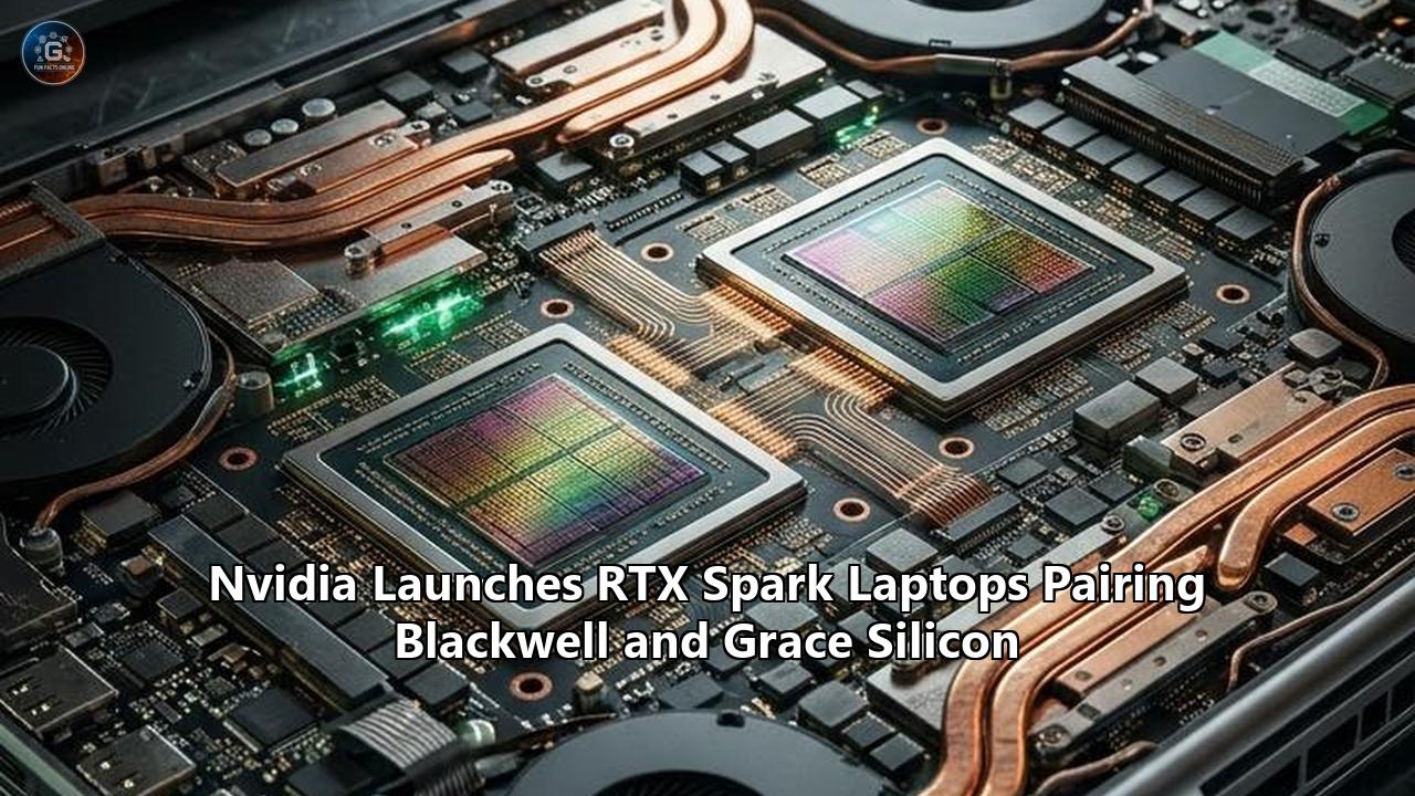
Commercial shipments of a new computing architecture began reaching consumers and enterprise developers on October 16, 2026, as six PC manufacturers released retail hardware powered by Nvidia’s N1X silicon platform. The commercial arrival of Nvidia RTX Spark laptops signals an aggressive bid to reshape personal computing, pairing Nvidia’s proprietary Arm-based Grace central processor with its Blackwell graphics architecture on a single, unified-memory substrate.
Led by Microsoft’s newly minted Surface Laptop Ultra—priced at $2,599 for baseline configurations and climbing beyond $5,800 for top-tier implementations—the platform introduces desktop supercomputing principles to mobile form factors. Hardware partners Asus, Dell, HP, Lenovo, and MSI simultaneously opened retail availability for their own variants, deploying a dual-die package fabricated on TSMC’s 3-nanometer node. Operating within an adjustable 45-to-80-watt thermal envelope, the flagship processor combines a 20-core Grace CPU with a Blackwell GPU packing 6,144 CUDA cores, 192 fifth-generation Tensor Cores, and up to 128 gigabytes of coherent, low-power double data rate 5X (LPDDR5X) memory.
Nvidia rates the platform at one petaflop of FP4 artificial intelligence throughput. By linking the CPU and GPU across an on-package NVLink Chip-to-Chip (NVLink-C2C) interconnect capable of 600 gigabytes per second of bidirectional bandwidth, the architecture eliminates the physical bus bottleneck that has separated system RAM from graphics memory in personal computers for over three decades.
This launch resolves an engineering bottleneck that has fractured the client computing market since the emergence of generative models. Local execution of 70-billion to 120-billion-parameter neural networks previously required multi-GPU desktop workstations drawing upwards of 1,000 watts, while mobile users were forced to choose between the high-bandwidth unified memory of Apple's closed macOS ecosystem or the Windows x86 graphics ecosystem shackled by limited discrete video memory. By fusing a full-scale Blackwell accelerator with an energy-efficient Grace Arm CPU under Windows 11, Nvidia has entered the client silicon market not merely as an add-in component supplier, but as the architect of the entire computing engine.
                 NVIDIA N1X SYSTEM ARCHITECTURE
       +------------------------------------------------+
       |   Unified Coherent LPDDR5X (Up to 128GB)       |
       +------------------------------------------------+
                               |
            600 GB/s Bidirectional Coherent Bus
                               |
        +----------------------+----------------------+
        |                                             |
+-----------------------+             +-------------------------------+
|    NVIDIA GRACE CPU   |             |     NVIDIA BLACKWELL GPU      |
|  20 Neoverse V-Cores  |<----------->|    6,144 CUDA / 192 Tensor    |
| (MediaTek Co-Design)  | NVLink-C2C  |    5th-Gen Tensor Engine      |
+-----------------------+             +-------------------------------+
        |                                             |
        +----------------------+----------------------+
                               |
                 Windows on Arm / Prism Runtime
The trajectory leading to this launch represents a multi-year escalation spanning corporate realignments, microarchitectural experiments in hyperscale data centers, a covert silicon collaboration with MediaTek, and an extensive overhaul of the Windows operating system.
2020–2022: The Structural Impasse and the Death of the Add-in Model
The technical origin of the RTX Spark architecture stems from a structural crisis that Nvidia recognized early in the 2020s: the physical limits of the conventional PC bus architecture.
For nearly thirty years, the x86 personal computer relied on a split-memory paradigm. The central processor maintained its own pool of dynamic random-access memory (DRAM) connected through a motherboard memory controller, while the discrete graphics processing unit (dGPU) communicated across the peripheral component interconnect express (PCIe) bus to its own dedicated video RAM (VRAM). In traditional gaming and professional rasterization pipelines, this separation was manageable. Assets such as textures, geometry meshes, and shader programs were streamed across PCIe links into VRAM, where the graphics pipeline operated on them locally.
The rapid rise of large language models (LLMs) and transformer-based diffusion architectures broke this paradigm. Transformers require immediate, random access to dozens or hundreds of billions of numerical parameters. In a split-memory system, if a model's weights exceed the discrete GPU's VRAM buffer—historically capped at 8GB, 16GB, or 24GB on consumer mobile hardware—inference falls off an operational cliff. Offloading unallocated layers across PCIe 4.0 or PCIe 5.0 back to host system RAM introduces latency penalties of two orders of magnitude, collapsing token generation speeds from conversational rates down to fractions of a word per second.
TRADITIONAL x86 SPLIT MEMORY (PCIe Bottleneck)
[ System DRAM ] <--> [ x86 Host CPU ] <=== PCIe 4.0/5.0 (32-64 GB/s) ===> [ GPU VRAM ] <--> [ Discrete GPU ]
                                                   ^
                                     Latency & Throughput Chokepoint

NVIDIA RTX SPARK UNIFIED MEMORY (NVLink-C2C)
+---------------------------------------------------------------+
|         Unified Physical Memory Pool (Up to 128GB)            |
+---------------------------------------------------------------+
                               |
       Cache-Coherent Shared Fabric (600 GB/s Bidirectional)
                               |
            +------------------+------------------+
            |                                     |
    [ Grace Arm CPU ]                     [ Blackwell GPU ]
Nvidia previously attempted to solve its dependence on third-party host architectures through acquisition. In September 2020, Nvidia announced an agreement to purchase Arm Ltd. from SoftBank Group for $40 billion. The acquisition aimed to give Nvidia total control over the world's most ubiquitous processor instruction set architecture (ISA), clearing a path to build tightly integrated, heterogeneous systems pairing Arm CPUs directly with Nvidia GPUs from edge devices to enterprise servers.
Over the subsequent eighteen months, regulatory scrutiny dismantled the deal. The US Federal Trade Commission sued to block the merger in December 2021, citing concerns over competition in data center infrastructure and edge computing. Counterparts in the United Kingdom (the Competition and Markets Authority) and the European Commission initiated exhaustive Phase II investigations. Competitors argued that Nvidia would inevitably prioritize its own hardware integrations at the expense of third-party Arm licensees. In February 2022, Nvidia and SoftBank formally abandoned the transaction.
The regulatory collapse forced a shift in Nvidia’s platform engineering. The company could not own the Arm architecture outright, but it retained an Arm architectural license. Rather than abandoning its custom CPU roadmap, Nvidia accelerated development within its enterprise infrastructure division. The corporate mandate was unambiguous: if Nvidia could not purchase an existing client ecosystem, it would build an alternative custom processor platform, prove it at scale in data center clusters, and ultimately miniaturize it for client machines.
2022–2024: Proving the Coherent Substrate in the Data Center
The architectural foundation that defines the new laptop line did not originate on a mobile drafting board; it was forged in enterprise server racks.
In 2022, Nvidia revealed the Grace CPU and the GH200 Grace Hopper Superchip. Grace was an Armv9-A enterprise processor featuring 72 Neoverse V2 cores, built to address high-performance computing (HPC) and massive-scale AI workloads. What made Grace distinct was not merely its compute density, but its interconnect: NVLink-C2C.
DATA CENTER PROVING GROUND (2022-2024)
+------------------------------------------------------------------------+
| GH200 / GB200 Enterprise Superchips                                   |
|   - 72-core Grace Armv9 Neoverse CPU                                   |
|   - NVLink-C2C (900 GB/s bidirectional coherent interface)            |
|   - LPDDR5X / HBM memory pools operating under a shared address space  |
|                                                                        |
| Key Engineering Validations:                                           |
|   1. Hardware cache coherency across disparate execution units        |
|   2. Zero-copy pointer exchange between CPU and GPU kernels            |
|   3. System-level stability under sustained 700W+ enterprise loads     |
+------------------------------------------------------------------------+
                                   |
                    Miniaturization Mandate (2024)
                                   v
+------------------------------------------------------------------------+
| N1X Client Architecture (RTX Spark)                                   |
|   - 18 to 20 custom Grace cores (MediaTek low-power PHY/IMC co-design) |
|   - NVLink-C2C scaled to 600 GB/s within a 45W-80W package             |
|   - 128GB LPDDR5X unified substrate replacing discrete VRAM            |
+------------------------------------------------------------------------+
NVLink-C2C delivered an ultra-wide, low-latency physical link that made disparate silicon dies function as a logically unified system-on-a-chip (SoC). Operating at up to 900 gigabytes per second in enterprise configurations, the interface provided full hardware cache coherency. The CPU and GPU could simultaneously address the same memory pool without explicit data transfers, software-level memory pinned buffers, or redundant copies across an external bus.
When the Blackwell architecture followed in early 2024 with the GB200 NVL72 rack-scale systems, the Grace-Blackwell coupling proved itself across hundreds of thousands of operational nodes. By pooling memory across high-speed interconnects, Nvidia allowed models with hundreds of billions of parameters to execute across unified address spaces with minimal inter-die communication overhead.
While the enterprise division absorbed massive capital allocations, engineers within Nvidia's personal systems group began investigating how this architecture could be scaled down. The primary technical hurdle was thermal dissipation and power efficiency. A dual-socket enterprise node consuming 700 to 1,200 watts can accommodate active liquid cooling and deep trace routing on complex multi-layer server boards. Translating that architecture into a notebook chassis requiring sub-80-watt total system consumption, air cooling, and commercial manufacturing yields necessitated a complete overhaul of the physical layer (PHY), the memory controller, and the power management circuitry.
By mid-2023, rumors circulated within the semiconductor supply chain that Nvidia was actively staffing client CPU software teams. In October 2023, Reuters published an investigative report confirming that Nvidia had quietly begun designing central processing units based on Arm architecture to run Microsoft's Windows operating system. Crucially, the reporting noted that an exclusive supplier agreement between Microsoft and Qualcomm—which had granted Qualcomm an effective monopoly on official Windows on Arm platform development—was scheduled to expire toward the end of 2024.
The regulatory clock was ticking down. The technical viability of the unified superchip had been validated in enterprise data centers. What remained was the formation of a consumer-grade silicon pipeline capable of producing modern client processors at scale.
2024–2025: The Secret Silicon Alliance and Project DIGITS
Developing an ultra-low-power client processor required competencies outside Nvidia’s traditional expertise. While Nvidia possessed deep mastery of high-throughput GPU architecture, high-speed interconnects, and enterprise memory controllers, building an energy-efficient client platform demands granular power-state switching, low-latency mobile dynamic memory controllers, integrated display processing pipelines, and integrated wireless communications.
To bridge this engineering divide, Nvidia partnered with Taiwanese semiconductor designer MediaTek in early 2024. Operating under internal codenames N1 and N1X, engineering teams from Santa Clara and Hsinchu established a split-development model. MediaTek brought its expertise in low-power physical implementation, radio frequency (RF) integration, and mobile memory routing, having refined these domains across its Dimensity line of smartphone and automotive platforms. Nvidia retained ownership of the high-performance core architecture, the GPU execution engine, the NVLink-C2C bus adaptation, and the CUDA software layer.
                THE MEDIATEK & NVIDIA DIVISION OF SILICON
+--------------------------------------+--------------------------------------+
|        MediaTek Contributions        |         Nvidia Contributions         |
+--------------------------------------+--------------------------------------+
| - Low-power PHY implementation       | - Blackwell GPU Compute Engine       |
| - High-efficiency LPDDR5X IMC design | - Grace Neoverse Microarchitecture   |
| - DisplayPort / PCIe root bridges    | - NVLink-C2C Interconnect Fabric     |
| - Wi-Fi 7 / Bluetooth 5.4 RF blocks  | - Tensor Core Engine & FP4 Precision |
| - Sub-system power gating & DVFS     | - CUDA & TensorRT Silicon Primitives |
+--------------------------------------+--------------------------------------+
The first public sign of this hardware miniaturization emerged at the Consumer Electronics Show in Las Vegas in January 2025. During an executive keynote, Nvidia showcased a compact prototype machine codenamed "Project DIGITS". Framed as an experimental personal workstation for AI developers, the device was housed in an aluminum chassis roughly the volume of a desktop book.
Internally, Project DIGITS ran on an early realization of the Grace Blackwell superchip, designated the GB10. It packed 128 gigabytes of coherent unified memory and claimed one petaflop of FP4 AI inference throughput, all operating beneath a compact cooling fan.
Industry reaction at the time was divided. Enterprise analysts viewed DIGITS as a specialty niche product—a luxury workstation for AI developers tired of renting cloud instances to debug small models. However, silicon forensics revealed a different intent. The GB10 was not a cut-down server board; its memory layout, single-package physical envelope, and dynamic power scaling were explicitly engineered around laptop board constraints.
In September 2025, during an investor forum, Nvidia Chief Executive Jensen Huang addressed questions regarding the commercial lifespan of Project DIGITS, which had been branded as DGX Spark for developer markets. Huang noted that the underlying architecture was not confined to desktop boxes, remarking that the integration of Grace and Blackwell at low operational wattages represented a general-purpose computing platform rather than a transient workstation experiment. Supply-chain tracking soon confirmed that test wafers carrying the N1X designation were running through TSMC's packaging lines in southern Taiwan, paired directly with advanced thermal vapor-chamber designs destined for laptop original design manufacturers (ODMs) such as Quanta, Compal, and Wistron.
The Computex 2026 Turning Point: Announcing RTX Spark
The formal introduction of Nvidia RTX Spark laptops as a consumer and workstation reality occurred on May 31, 2026, during the GTC Taipei keynote ahead of Computex.
Jensen Huang took the stage alongside Microsoft Chief Executive Satya Nadella to outline what both executives characterized as a fundamental disruption of the personal computing landscape. For over four decades, the Windows PC had operated under an architectural division of labor established by Intel and sustained by AMD: x86 instruction execution on the CPU, with graphics processing handled via attached acceleration units. Even the arrival of Copilot+ PCs in mid-2024 had preserved a rigid taxonomy: low-power neural processing units (NPUs) delivering 40 to 50 tera-operations per second (TOPS) handled background tasks like video background blurring and audio filtering, but lacked the raw memory bandwidth and compute density required to run high-parameter intelligence models locally.
Nadella and Huang unveiled the platform under its official commercial name: Nvidia RTX Spark.
               THE LOCAL COMPUTING EVOLUTION
+-----------------------------------------------------------------------+
| PHASE 1: The Cloud-Dependent Paradigm (2022-2024)                     |
| Architecture: Thin clients sending prompts over the internet          |
| Constraints: Cloud token latency, ongoing API costs, privacy concerns |
+-----------------------------------------------------------------------+
                                   |
                                   v
+-----------------------------------------------------------------------+
| PHASE 2: The Constrained NPU "Copilot+ PC" (2024-2025)                |
| Architecture: x86/Arm CPU + Low-power 45 TOPS NPU                     |
| Constraints: Limited to small vision/audio tasks, toy SLMs (<3B params)|
+-----------------------------------------------------------------------+
                                   |
                                   v
+-----------------------------------------------------------------------+
| PHASE 3: The Unified Superchip "RTX Spark" (2026)                     |
| Architecture: Grace Arm CPU + Blackwell GPU + 128GB Unified Memory    |
| Capabilities: 1,000 TOPS (1 PFLOPS FP4), local 120B+ parameter agents  |
+-----------------------------------------------------------------------+
The pitch addressed the core architectural dilemma facing technical buyers: users who wanted serious, local AI execution were previously forced to purchase Apple Silicon hardware to secure large unified memory pools, thereby abandoning native Windows support and the expansive CUDA enterprise library. Alternatively, buyers could purchase high-end Windows gaming laptops equipped with mobile GeForce RTX 4090 or 5090 GPUs, only to find themselves hard-capped by 16GB or 24GB of discrete VRAM.
RTX Spark presented a resolution to that trade-off:
- A native Windows 11 platform running on high-efficiency Arm architecture;
- Total physical unification of system and graphics memory up to 128GB;
- Native execution across the entire Nvidia CUDA and TensorRT software ecosystem.
During the Taipei keynote, Microsoft unveiled the flagship execution of the architecture: the Surface Laptop Ultra. Characterized by an ultra-slim chassis, dynamic active cooling, and a complete absence of an x86 processor, the Surface Laptop Ultra served as the validation platform for Microsoft's vision of local, autonomous "personal agents".
Nvidia announced that retail systems would arrive globally in mid-October 2026, supported by an array of manufacturing partners: Asus, Dell, HP, Lenovo, Microsoft, and MSI. In parallel, Nvidia outlined plans for compact desktop implementations to ship in November, providing developers with continuous, 24/7 background agent execution in sub-liter form factors.
The Software Engineering Blitz: Preparing Windows on Arm for CUDA
Announcing hardware is an engineering challenge; establishing full-stack software viability across a non-native architecture is a larger operational undertaking. Between the Computex reveal in May and the retail launch in October, Nvidia, Microsoft, and an army of open-source maintainers executed an intensive software migration effort.
The historical hurdle for Windows on Arm had always been software compatibility. Early Windows on Arm devices had foundered on sluggish emulation, incomplete peripheral driver ecosystems, and absent software developer tools. While Microsoft’s 2024 introduction of the Prism emulation engine had addressed standard 64-bit x86 (x64) desktop applications, the scientific and AI computing ecosystems relied on deeply specialized compilation pipelines, native hardware drivers, and low-level kernel extensions that could not tolerate emulation overhead.
               RTX SPARK SOFTWARE INFRASTRUCTURE
+---------------------------------------------------------------+
|  Local Autonomous Agents (GitHub Copilot, Pi, OpenClaw, Hermes)|
+---------------------------------------------------------------+
|  Agent Orchestration Layer: NVIDIA OpenShell / NemoClaw       |
+---------------------------------------------------------------+
|  Framework Layer: PyTorch-CUDA for ARM64, TensorRT-LLM, ONNX   |
+---------------------------------------------------------------+
|  Environment Layer: Native Conda, Python 3.15 Universal ABI   |
+---------------------------------------------------------------+
|  OS & Emulation Layer: Windows 11 on Arm + Prism Translation   |
+---------------------------------------------------------------+
|  Silicon Layer: N1X Hardware (Grace CPU + Blackwell GPU)      |
+---------------------------------------------------------------+
Over the summer of 2026, Nvidia and Microsoft rolled out six architectural software pillars designed to ensure zero-day viability for developers and data scientists:
1. PyTorch-CUDA Native ARM64 Build
For the first time in Windows computing history, Nvidia upstreamed official, production-ready PyTorch packages compiled natively for ARM64 Windows with integrated CUDA acceleration. Previously, running PyTorch on an Arm-powered Windows device meant compiling via CPU-only fallbacks or enduring the severe latency penalties of emulated x64 runtime environments. The native ARM64 build enabled execution on Grace CPU cores while offloading tensor mathematics straight to Blackwell Tensor Cores with zero virtualization overhead.
2. Universal Python and Conda Integration
Data science workflows are tethered to the Conda package management system and the Python runtime ecosystem. Nvidia and Microsoft partnered with Anaconda to deliver a native ARM64 Conda installer and built native binaries for more than 2,000 foundational scientific packages. Official telemetry published by Nvidia indicated that 97% of the top 15,000 Python packages were verified to run natively on the Windows on Arm platform without compilation warnings.
3. Unified Memory Driver Allocators
In traditional computing platforms, software applications explicitly declare whether a variable or data structure resides in host RAM or device VRAM using calls such as cudaMalloc() and malloc(). Nvidia introduced an updated unified memory driver for Windows 11 that abstracts this allocation boundary. Memory buffers declared in Python or C++ are pinned directly within the physical LPDDR5X address space, allowing both the Grace CPU and Blackwell GPU to mutate the same memory structures without serialization or inter-device memory copying.
4. Agent Sandboxing with OpenShell and Execution Containers
Recognizing the security implications of running autonomous coding agents locally—agents that read, write, and execute shell scripts—Nvidia partnered with Microsoft to deploy "NVIDIA OpenShell" alongside Windows Execution Containers. This software subsystem implements hardware-enforced virtualization boundaries around autonomous agents like OpenClaw, Hermes, and GitHub Copilot, ensuring that autonomous code generation operates within isolated memory spaces while retaining access to the unified Tensor Core hardware pipeline.
5. Hybrid Prompt Routing Engines
To maximize energy efficiency when running on battery power, the software stack integrates an intelligent inference router. When an autonomous agent queries an underlying model, the router evaluates context length and reasoning complexity. Low-complexity tasks are routed to localized small language models (SLMs) such as Microsoft’s MAI-Code-1.1-Flash running on device; high-complexity edge cases can be escalated to remote data centers via an API bridge, minimizing battery drain while preserving conversational responsiveness.
6. Gaming and Creative Driver Translation
To ensure consumers were not alienated by the shift to Arm, Nvidia deployed native Windows on Arm display drivers featuring full feature parity with its desktop Game Ready and Studio drivers. This included full integration of DirectX 12 Ultimate, Vulkan, and Nvidia DLSS 5. Legacy x86 gaming titles run through Microsoft’s optimized Prism translation layer, which dynamically intercepts x86 instructions and translates them to Arm64 instructions, while native GPU API calls pass directly to the Blackwell execution pipeline.
Hardware Teardown: Inside the N1X Superchip
On October 8, 2026, Nvidia hosted an technical briefing in San Francisco, providing microarchitectural specifications for the N1X superchip that powers the RTX Spark platform.
               N1X DUAL-DIE PHYSICAL FLOORPLAN
+---------------------------------------------------------------+
| TSMC 3nm Substrate Package                                     |
|                                                               |
|  +---------------------------+   +-------------------------+  |
|  |     GRACE CPU DIE         |   |    BLACKWELL GPU DIE    |  |
|  |                           |   |                         |  |
|  | [16x Neoverse Performance]|   | [6,144 FP32 CUDA Cores] |  |
|  | [4x Neoverse Efficiency]  |   | [192 5th-Gen Tensor]    |  |
|  | [24MB Shared System Cache]|   | [48 Ray Tracing Units]  |  |
|  +---------------------------+   +-------------------------+  |
|                ^                              ^               |
|                |                              |               |
|                +====== NVLink-C2C Bus ========+               |
|                       (600 GB/s Bidirectional)                |
|                                                               |
|  +---------------------------------------------------------+  |
|  |      Coherent LPDDR5X-8533 Memory Subsystem             |  |
|  |      512-bit Interface | 546 GB/s Peak Bandwidth        |  |
|  |      Capacities: 24GB, 64GB, or 128GB                   |  |
|  +---------------------------------------------------------+  |
+---------------------------------------------------------------+
The silicon package is a multi-chip module (MCM) fabricated using TSMC’s advanced 3nm (N3P) lithography process. It integrates two primary compute complexes wired directly together on a high-density organic substrate: the Grace CPU complex and the Blackwell GPU complex.
The Grace Client CPU Complex
The Grace processor powering RTX Spark is configured in two distinct tiers, depending on the thermal and pricing segment of the host laptop:
- The Flagship Tier: Features 20 64-bit Armv9-A CPU cores arranged in an asymmetric configuration. The performance cluster consists of 16 high-throughput Neoverse cores featuring dual 256-bit Scalable Vector Extension 2 (SVE2) units, 2MB of dedicated L2 cache per core, and aggressive out-of-order execution pipelines. The efficiency cluster incorporates 4 low-power Neoverse cores designed to handle operating system housekeeping and background processes with minimal dynamic power leakage.
- The Mainstream Tier: Utilizes an 18-core layout, scaling the performance core count to 14 while preserving the 4 efficiency cores.
Both tiers feature a unified 24MB shared system-level cache that serves as an intermediate buffer prior to memory bus access, mitigating latency when the CPU interacts with tensors residing in the primary memory pool.
The Blackwell RTX Mobile GPU Complex
The graphics and tensor execution engine inside the N1X is an architectural direct descendant of Nvidia’s enterprise Blackwell silicon.
- Compute Units: The primary configuration contains 48 Streaming Multiprocessors (SMs). With 128 FP32 arithmetic logic units per SM, the chip boasts a total of 6,144 CUDA cores.
- Fifth-Generation Tensor Cores: Each SM contains four fifth-generation Tensor Cores, totaling 192 Tensor Cores. These units introduce microscopic precision capabilities, running FP8, FP6, and native FP4 tensor operations. The inclusion of FP4 precision is the foundational mechanism that allows the chip to achieve one petaflop of AI compute within an 80-watt total power budget.
- Ray Tracing Infrastructure: 48 third-generation RT Cores provide hardware-accelerated bounding volume hierarchy (BVH) traversal and ray-triangle intersection testing, ensuring that laptops can handle complex path-traced rendering pipelines and gaming workloads.
- Secondary Configuration: The lower-tier mobile variant reduces the SM count to 40, fielding 5,120 CUDA cores and 160 Tensor Cores.
           N1X SILICON CONFIGURATION MATRIX
+----------------------------+-----------------------+-----------------------+
| Metric / Feature           | Flagship N1X Tier     | Mainstream N1X Tier   |
+----------------------------+-----------------------+-----------------------+
| Lithography Node           | TSMC 3nm (N3P)        | TSMC 3nm (N3P)        |
| CPU Core Layout            | 20 Cores (16P + 4E)   | 18 Cores (14P + 4E)   |
| CPU Architecture           | Armv9-A Neoverse      | Armv9-A Neoverse      |
| GPU CUDA Cores             | 6,144 Cores           | 5,120 Cores           |
| 5th-Gen Tensor Cores       | 192 Units             | 160 Units             |
| Ray Tracing (RT) Cores     | 48 Units              | 40 Units              |
| Memory Capacities          | Up to 128GB LPDDR5X   | 24GB to 64GB LPDDR5X  |
| Memory Interface Width     | 512-bit               | 256-bit or 512-bit    |
| Peak Memory Bandwidth      | 546 GB/s              | 273 - 546 GB/s        |
| Interconnect Bandwidth     | 600 GB/s (NVLink-C2C) | 600 GB/s (NVLink-C2C) |
| Target Power Envelope(TDP) | 45W - 80W             | 35W - 65W             |
| Peak FP4 AI Performance    | 1 PFLOPS (1,000 TOPS) | ~800 TFLOPS (FP4)     |
+----------------------------+-----------------------+-----------------------+
The Interconnect and Unified Memory Subsystem
The core of the N1X platform is its interconnect and unified memory architecture. The CPU and GPU communicate across a mobile realization of NVLink-C2C. Routing across thousands of microscopic copper interconnects on the package substrate, this bus delivers 600 gigabytes per second of raw, bidirectional bandwidth at less than 1.5 picojoules per bit.
This interconnect enables cache-coherent access to a shared memory pool consisting of low-power LPDDR5X-8533 memory. Utilizing a 512-bit wide memory interface, the subsystem delivers a continuous memory bandwidth of 546 gigabytes per second. Unlike traditional laptop architectures, there is no physical segregation between CPU system memory and GPU frame buffer memory. If an AI developer loads a 95-gigabyte quantized large language model into memory, the entire buffer is directly accessible by the Blackwell GPU for tensor calculation, while the Grace CPU performs token sampling and context scheduling in the exact same memory space without performing any bus transfers.
Retail Availability and OEM Implementations
When retail availability commenced on October 16, 2026, the device catalog demonstrated broad adoption of the superchip platform. Across the launch fleet, Nvidia RTX Spark laptops manifest in divergent thermal envelopes, mechanical enclosures, and target markets.
                     OCTOBER 2026 LAUNCH HARDWARE LINEUP
+-----------------------+----------------+-------------+------------+--------------------+
| Device Model          | CPU/GPU Config | Memory      | Base Price | Target Segment     |
+-----------------------+----------------+-------------+------------+--------------------+
| MS Surface Laptop     | 20-Core /      | 64GB or     | $2,599     | Executive, AI Dev, |
| Ultra                 | 6,144 CUDA     | 128GB       |            | Mobile Creator     |
+-----------------------+----------------+-------------+------------+--------------------+
| Dell XPS 16 Spark     | 20-Core /      | Up to 128GB | $2,799     | Enterprise Systems,|
| Edition               | 6,144 CUDA     |             |            | Data Science       |
+-----------------------+----------------+-------------+------------+--------------------+
| Asus ROG Zephyrus G16 | 20-Core /      | 64GB or     | $2,499     | High-End Gaming,   |
| Spark                 | 6,144 CUDA     | 128GB       |            | Local AI Dev       |
+-----------------------+----------------+-------------+------------+--------------------+
| Lenovo ThinkPad P1    | 20-Core /      | 128GB ECC-  | $3,199     | Workstation /      |
| Gen 8 Spark           | 6,144 CUDA     | capable     |            | CAD / Financial    |
+-----------------------+----------------+-------------+------------+--------------------+
| HP OmniBook Ultra     | 18-Core /      | 32GB or     | $1,999     | Prosumer /         |
| Studio                | 5,120 CUDA     | 64GB        |            | Creative           |
+-----------------------+----------------+-------------+------------+--------------------+
| MSI CreatorPro S16    | 20-Core /      | 128GB       | $2,699     | Studio Production, |
| Spark                 | 6,144 CUDA     |             |            | 3D Visualization   |
+-----------------------+----------------+-------------+------------+--------------------+
Microsoft Surface Laptop Ultra
Microsoft positioned the Surface Laptop Ultra as the flagship embodiment of the platform. Built inside a CNC-machined magnesium-aluminum unibody measuring 0.55 inches thick and weighing 3.1 pounds, the device is configured strictly with the flagship 20-core Grace CPU and 6,144-core Blackwell GPU. Microsoft offers two primary configurations:
- A 64GB unified memory variant priced at $2,599.99.
- A 128GB unified memory variant paired with a 4TB self-encrypting solid-state drive, carrying a retail price of $5,899.99.
The Surface Laptop Ultra incorporates a 14.4-inch PixelSense Flow display running at 3120x2080 with a 144Hz variable refresh rate. Cooling is managed by an ultra-thin dual vapor-chamber assembly using graphite spreaders to sustain an 80-watt package dissipation during continuous inference passes.
Dell XPS 16 Spark Edition
Dell aligned its implementation with the enterprise developer and data science community. The XPS 16 Spark Edition preserves the minimalist glass-and-aluminum design of the XPS family, integrating the 20-core N1X platform with standard 128GB LPDDR5X configurations. Dell engineers placed specific emphasis on silent acoustics, utilizing a custom liquid-crystal polymer fan array that keeps operational noise below 32 decibels during sustained FP4 model inference. The machine starts at $2,799.
Asus ROG Zephyrus G16 Spark
Targeted directly at high-end gamers and independent software developers, Asus paired the N1X superchip with a 240Hz 2.5K OLED panel. By deploying liquid metal thermal interfaces on both the Grace and Blackwell dies, Asus configured the platform to maintain its peak 80-watt TDP profile over sustained gaming sessions. The machine is equipped with dual USB4 / Thunderbolt 4 ports, a full-sized SD Express card reader, and retail pricing starting at $2,499 for a 64GB configuration.
Lenovo ThinkPad P1 Gen 8 Spark
Focusing squarely on certified CAD, financial modeling, and engineering workloads, Lenovo deployed the 20-core Grace processor inside a carbon-fiber-reinforced enclosure. The ThinkPad P1 Spark integrates hardware ECC-like data integrity checks over its 128GB memory bus, offers an optional anti-glare touch display, and includes independent software vendor (ISV) certifications for software suites such as Dassault Systèmes SOLIDWORKS, Autodesk Maya, and ESRI ArcGIS. The base enterprise configuration retails at $3,199.
HP and MSI Implementations
HP introduced the OmniBook Ultra Studio, an 18-core variant aimed at prosumers, with 32GB and 64GB configurations priced aggressively starting at $1,999 to capture mainstream creators. Concurrently, MSI shipped the CreatorPro S16 Spark, targeting studio visual effects artists and indie game developers with a thermal package tuned for continuous 3D rendering in Unreal Engine 5.4, priced at $2,699 with 128GB of unified RAM.
Technical Benchmarks and Comparative Analysis
Hardware evaluations conducted across production units highlight the architectural divergence between unified superchips and traditional computing platforms. Testing yields concrete metrics across local AI execution, 3D rendering pipelines, standard productivity compilation, and battery runtimes.
             AI INFERENCE: TIME TO FIRST TOKEN (SECONDS)
                   (Lower is Better / Model: Qwen-3.5 27B)
+---------------------------------------------------------------+
| RTX Spark (N1X 128GB)         [1.12s]                         |
| Apple M5 Pro (16" MacBook)    [2.35s]                         |
| AMD Ryzen AI Max+ 395         [3.42s]                         |
| Intel Panther Lake 12Xe       [5.15s]                         |
+---------------------------------------------------------------+

             LOCAL CODING AGENT WORKFLOW THROUGHPUT
                (Higher is Better / Metric: Relative Index)
+---------------------------------------------------------------+
| RTX Spark (N1X 128GB)         [4.6x]                          |
| Apple M5 Pro                  [2.2x]                          |
| AMD Ryzen AI Max+ 395         [1.8x]                          |
| Intel Panther Lake 12Xe       [1.0x Baseline]                 |
+---------------------------------------------------------------+

             3D GRAPHICS: 3DMARK STEEL NOMAD LITE
                   (Higher is Better / Metric: FPS)
+---------------------------------------------------------------+
| RTX Spark (N1X 128GB)         [98.29 FPS]                     |
| Asus ROG Flow (Ryzen AI Max+) [48.12 FPS]                     |
| Lenovo IdeaPad (Core Ultra X9)[46.07 FPS]                     |
+---------------------------------------------------------------+
Local Artificial Intelligence Performance
The core value proposition of the N1X platform lies in local inference throughput. When benchmarking time-to-first-token (TTFT) using llama.cpp on the Qwen3.5 27-billion parameter instruct model, the Surface Laptop Ultra achieved a response latency of 1.12 seconds. By comparison, a 16-inch MacBook Pro configured with Apple's M5 Pro silicon recorded 2.35 seconds under identical quantization profiles—giving the N1X a 2.1x advantage in responsiveness.
The performance delta widens on generative diffusion workflows. In ComfyUI executing FLUX.2 Klein (a 4-billion parameter image generation transformer), the Blackwell GPU's fifth-generation Tensor Cores and wide 546 GB/s memory bandwidth completed standard 20-step generation in 2.1 seconds, compared to 9.0 seconds on an Apple M5 Pro (a 4.3x performance multiplier).
On complex local video generation utilizing LTX-2.3 (a 22-billion parameter video diffusion model), the Surface Laptop Ultra maintained an output rate 5.4x to 6.2x faster than the M5 Pro, which suffered thermal throttling due to sustained unified memory saturation.
                     BENCHMARK COMPARISON MATRIX
+--------------------------+-------------+-------------+-------------+-------------+
| Benchmark Test           | RTX Spark   | Apple M5    | Intel P-Lake| AMD Ryzen   |
|                          | N1X (128GB) | Pro (48GB)  | 12Xe (32GB) | Max+ 395    |
+--------------------------+-------------+-------------+-------------+-------------+
| TTFT: Qwen3.5 27B (s)    | 1.12s       | 2.35s       | 5.15s       | 3.42s       |
| FLUX.2 Klein 4B Gen (s)  | 2.1s        | 9.0s        | 14.8s       | 8.9s        |
| LTX-2.3 22B Video (Rel)  | 5.4x        | 1.0x (Base) | N/A (OOM)   | 1.2x        |
| Coding Agent Speed (Rel) | 4.6x        | 2.2x        | 1.0x (Base) | 1.8x        |
| 3DMark Steel Nomad Lite  | 98.29 FPS   | N/A (macOS) | 46.07 FPS   | 48.12 FPS   |
| 3DMark Speed Way (RT)    | 30.31 FPS   | N/A (macOS) | 12.14 FPS   | 19.72 FPS   |
| Continuous Agent Battery | 14.2 Hours  | 16.5 Hours  | 7.8 Hours   | 9.4 Hours   |
+--------------------------+-------------+-------------+-------------+-------------+
When evaluated against Intel’s flagship mobile x86 architecture—the Panther Lake platform featuring integrated 12Xe graphics—Nvidia's data demonstrates a 4.6x performance advantage in running multi-step autonomous coding agents, a 2.7x speedup during local model fine-tuning with LoRA (Low-Rank Adaptation), and a 1.8x advantage in code compilation times.
Graphics and Synthetic Compute
Graphics performance validates Nvidia’s decision to embed a complete Blackwell accelerator rather than an integrated mobile GPU.
- In 3DMark Steel Nomad Lite, the Surface Laptop Ultra yielded 98.29 frames per second. This result more than doubles the 46.07 FPS output by Lenovo's Intel Core Ultra X9 IdeaPad Pro 5.
- In 3DMark Speed Way, a demanding test exercising full ray tracing, DirectX 12 Ultimate variable-rate shading, and complex lighting bounces, the N1X posted 30.31 FPS. By contrast, the Asus ROG Flow Z13, configured with AMD's Ryzen AI Max+ 395 processor featuring Radeon 8060S graphics, attained 19.72 FPS—a 53% victory for the Blackwell silicon.
In actual gaming environments, running Cyberpunk 2077 at 1440p resolution with the Ray Tracing Ultra preset, the N1X platform sustained 104 frames per second when utilizing DLSS 5 with 3D-Guided Neural Rendering and Frame Generation. Games reliant on high polygon counts and large memory pools, such as Microsoft Flight Simulator 2024 and NBA 2K27, operated without memory stuttering, as the 128GB unified memory pool eliminated the asset streaming hitches that occur on conventional 16GB discrete mobile graphics cards.
Thermal Characteristics and Battery Longevity
The Grace CPU complex delivers energy metrics typical of Arm architectures. Under standard office productivity workloads, such as web navigation across dozens of browser tabs, document editing, and video streaming, the Surface Laptop Ultra drew an average of 4.8 watts from its 75-watt-hour battery, translating to 17.5 hours of continuous runtime.
Under sustained AI agent development—where an autonomous background model continuously parses code edits, generates unit tests, and verifies compilation—the platform sustained an operational battery life of 14.2 hours. Under equivalent agent-loop executions, Intel Panther Lake systems exhausted their batteries in 7.8 hours, while AMD Strix Halo configurations drained in 9.4 hours. The Apple MacBook Pro with M5 Pro remained the sole competitor to outlast the N1X on pure battery duration, delivering 16.5 hours of light execution, though it did so while trailing the N1X's local model generation throughput.
Market Dynamics: Shifting the Balance of Client Silicon
The retail debut of the N1X platform permanently disrupts competitive alignments across the personal computer industry. By entering the market with an integrated CPU and GPU system platform, Nvidia ceases to be merely a high-margin component supplier to the x86 duopoly and transforms into an end-to-end platform vendor.
                     THE CLIENT SILICON MATRIX (POST-OCTOBER 2026)
+------------+--------------------+------------------------+------------------------------------+
| Company    | Architecture Model | Primary Defensible Moat| Strategic Exposure                 |
+------------+--------------------+------------------------+------------------------------------+
| NVIDIA     | Arm + Blackwell    | CUDA, 128GB Unified    | High entry pricing ($2,599+),      |
|            | Unified Superchip  | Memory, Enterprise AI  | dependency on TSMC 3nm capacity    |
+------------+--------------------+------------------------+------------------------------------+
| INTEL      | x86 Disaggregated  | Enterprise IT fleets,  | Lack of high-bandwidth unified     |
|            | Multi-Tile (P-Lake)| legacy validation      | memory; lagging FP4 AI throughput  |
+------------+--------------------+------------------------+------------------------------------+
| AMD        | x86 Monolithic /   | Open ROCm initiatives, | Squeezed between Intel volume and  |
|            | Chiplet APU (Halo) | console semi-custom    | Nvidia CUDA developer dominance   |
+------------+--------------------+------------------------+------------------------------------+
| QUALCOMM   | Arm SoC (Oryon)    | Sub-$1,000 mainstream  | Excluded from workstation/gaming;  |
|            | Discrete NPU       | mobile battery life    | low memory bandwidth ceiling       |
+------------+--------------------+------------------------+------------------------------------+
| APPLE      | Custom Arm SoC     | macOS ecosystem,       | Break of its exclusive claim on    |
|            | Unified Apple GPU  | vertical integration   | portable unified-memory computing  |
+------------+--------------------+------------------------+------------------------------------+
The Impact on Intel and AMD
For two decades, Intel and AMD accommodated Nvidia’s growing graphical influence because every GeForce graphics card sold required an accompanying x86 central processor. Even as Nvidia captured the high-margin margins of gaming notebooks, Intel and AMD retained ownership of the host platform, the core operating system interrupts, and corporate enterprise purchasing relationships.
The RTX Spark architecture challenges that dynamic. By pairing its Blackwell graphics engine exclusively with its own Grace Arm processor, Nvidia captures 100% of the silicon content value within each machine sold.
Intel finds itself in a precarious position. While its Panther Lake processor line has achieved improvements in transistor efficiency through its Intel 18A lithography process, its graphics processing tiles remain insufficient for high-parameter tensor workloads, and its disaggregated packaging cannot deliver 546 GB/s of shared memory bandwidth without skyrocketing package costs.
AMD, meanwhile, faces pressure on its high-end APU strategies. While AMD’s Ryzen AI Max+ (Strix Halo) platform attempted to deliver unified memory to x86 laptops using a wide 256-bit LPDDR5X bus, its compute architecture relies on ROCm—a developer software stack that continues to trail Nvidia’s CUDA in enterprise stability, software tool integrations, and plug-and-play machine learning library support.
The Disruption of Qualcomm’s Windows on Arm Position
When Microsoft launched its initial Copilot+ PC initiative in May 2024, Qualcomm was the exclusive silicon partner, fielding its Snapdragon X Elite processors. Qualcomm positioned itself as the definitive champion of Windows on Arm, pitching power efficiency and all-day battery life to mainstream business users.
The expiration of Qualcomm's exclusivity window, combined with Nvidia's entrance, relegates Qualcomm to the mainstream and budget segments of the Windows on Arm landscape. Qualcomm’s Oryon CPU architecture and Adreno graphics pipeline were engineered around smartphone and low-power ultrabook profiles; they cannot compete with the 6,144 CUDA cores, 192 Tensor Cores, and 128GB coherent memory pipelines of the N1X.
Nvidia has effectively captured the premium and workstation tiers of Windows on Arm, leaving Qualcomm to defend the sub-$1,200 commercial laptop market against emerging low-power x86 chips.
Breaking Apple’s Unified Memory Monopoly
From the moment Apple introduced the M1 processor family in late 2020 through the debut of the M4 and M5 series, Cupertino held an unchallenged marketing and technical advantage: unified, high-bandwidth LPDDR memory integrated directly into high-end notebooks.
Creative professionals, machine learning researchers, and visual effects artists routinely bought maxed-out MacBook Pros containing 64GB, 96GB, or 128GB of unified memory specifically because they could run local LLMs and massive 3D scenes that would crash a 16GB Windows laptop. Apple commanded massive gross margins on these memory upgrades, charging upwards of $400 for 16GB increments.
Nvidia RTX Spark laptops dismantle this monopoly. Creative professionals can now access up to 128GB of high-speed unified memory without forfeiting the Windows software ecosystem, DirectX gaming capabilities, or the ubiquitous CUDA development stack.
Furthermore, because Apple relies on Metal rather than CUDA, machine learning researchers running PyTorch on macOS have persistently faced missing operator kernels, delayed updates, and incomplete framework feature parity. The N1X offers those researchers native, zero-compromise CUDA execution alongside the memory capacities previously exclusive to Apple silicon.
Supply Chain Realities and System Economics
While technical evaluations validate the platform's processing power, commercial adoption faces near-term friction stemming from manufacturing costs, silicon packaging constraints, and retail pricing barriers.
                     ESTIMATED N1X BILL OF MATERIALS (BOM)
+-------------------------------------------------------------+
| TSMC 3nm Dual-Die Package & Packaging (CoWoS/Advanced MCM)  |
| [====================================] $620 - $750          |
|                                                             |
| Micron / Samsung 128GB LPDDR5X-8533 Unified Memory Stack    |
| [==============================] $400 - $480                 |
|                                                             |
| Dual-Chamber Copper Vapor Thermal Heat Exchanger Subsystem   |
| [======] $85 - $110                                         |
|                                                             |
| Power Delivery: Smart 16-Phase DrMOS VRM & Controller ICs   |
| [====] $65 - $80                                            |
|                                                             |
| MediaTek I/O, Subsystem Control, and Wi-Fi 7 / BT 5.4 Comms |
| [===] $45 - $60                                             |
+-------------------------------------------------------------+
| TOTAL ESTIMATED SILICON & SUBSYSTEM PLATFORM COST:          |
| $1,215 - $1,480                                             |
+-------------------------------------------------------------+
The Cost of the Unified Memory Architecture
The bill of materials (BOM) for an N1X superchip motherboard is among the highest ever recorded for a consumer mobile computer. Fabricating two complex logic dies on TSMC’s premium 3nm process node, integrating them via advanced packaging substrates, and soldering 128GB of top-bin LPDDR5X-8533 memory creates a hardware baseline cost estimated between $1,215 and $1,480 before an OEM builds the screen, chassis, keyboard, or battery.
This cost structure explains the starting prices announced across the OEM fleet. Baseline systems featuring cut-down 18-core processors and smaller 24GB or 32GB memory configurations command entry prices between $1,999 and $2,599.
For professionals requiring the flagship 20-core CPU, 6,144-core GPU, and the complete 128GB unified memory buffer, retail costs land between $3,200 and $5,900. Consequently, RTX Spark laptops will not initially achieve mass-market unit volumes; they represent specialized commercial and enthusiast capital investments targeting data scientists, software developers, creative studios, and well-funded early adopters.
Packaging Capacity Constraints
The second bottleneck lies in advanced semiconductor packaging capacity. While the N1X uses a simplified organic substrate rather than the ultra-complex Silicon-Interposer Chip-on-Wafer-on-Substrate (CoWoS-S) required by Nvidia’s hyperscale enterprise GB200 systems, it still competes for TSMC's advanced testing, multi-die placement, and high-density substrate lines.
Throughout early 2026, packaging availability has remained tight across the semiconductor supply chain. If enterprise demand for server-bound Blackwell accelerators surges, Nvidia may face internal resource allocation choices: prioritize enterprise GB200/GB300 compute boards carrying 75% gross margins, or supply consumer client N1X packages carrying 55% to 60% gross margins.
Industry analysts expect initial supply of 128GB laptop configurations to remain constrained throughout the fourth quarter of 2026, with stock stabilization arriving in the first quarter of 2027 as TSMC’s Fab 18 expansions in Tainan reach full yield output.
The Escalation Ahead: Desktops, GB300, and the Road to Autonomous Agents
The launch of portable laptops marks only the first phase of an operational rollout designed to establish local artificial intelligence computing across the entire Windows client fleet.
                 NVIDIA PERSONAL AI HARDWARE ROADMAP
+------------------------------------------------------------------------+
| OCTOBER 2026: Commercial Laptop Phase (Available Now)                 |
| Hardware: N1X Superchip (20-core Grace, 6,144 Blackwell CUDA, 128GB)   |
| Form Factor: 0.55" Notebooks (Surface Laptop Ultra, Dell XPS, ROG G16) |
| Focus: Local personal agents, mobile data science, mobile gaming       |
+------------------------------------------------------------------------+
                                   |
                                   v
+------------------------------------------------------------------------+
| NOVEMBER 2026: Compact Desktop Phase (Shipping Soon)                   |
| Hardware: N1X Desktop Substrate (80W Continuous, SFF Enclosures)       |
| Form Factor: 1.0-Liter to 2.5-Liter Desktop Appliances                 |
| Focus: 24/7 Always-On Local Agents, Persistent Workflow Automation     |
+------------------------------------------------------------------------+
                                   |
                                   v
+------------------------------------------------------------------------+
| EARLY 2027: Enterprise Desktop Supercomputing Phase                    |
| Hardware: GB300 Grace Blackwell Ultra Superchip                        |
| Specs: 748GB Unified Coherent Memory, 20 PFLOPS AI Compute             |
| Focus: Multi-Agent Swarms, Trillion-Parameter Local Model Development   |
+------------------------------------------------------------------------+
November 2026: The Compact Desktop Fleet
Following the portable laptop rollout, Nvidia and its manufacturing partners will ship compact desktop implementations of the RTX Spark platform in November 2026. Operating without the physical boundaries imposed by display panels and battery packs, these small-form-factor (SFF) desktop units—measuring roughly 150mm on each side—will run the N1X platform at its maximum 80-watt TDP profile indefinitely.
Designed to operate as persistent, headless "desk-side token appliances," these compact systems are intended to run local autonomous agents 24 hours a day, 7 days a week. Users can assign agents to monitor enterprise databases, summarize incoming client correspondence, scan repositories for security vulnerabilities, and handle local data processing tasks without sending unencrypted proprietary data over third-party cloud APIs.
Early 2027: The DGX Station for Windows (GB300)
For organizations that outgrow the 128GB memory ceiling and single-petaflop throughput of the mobile N1X platform, Nvidia has slated the top of the RTX Spark family for release in early 2027: the DGX Station for Windows.
This flagship desktop machine abandons the N1X silicon entirely in favor of Nvidia’s GB300 Grace Blackwell Ultra superchip. The workstation incorporates 748 gigabytes of coherent unified memory and delivers 20 petaflops of FP4 compute throughput.
Engineered to operate as a departmental "token engine," the DGX Station for Windows will execute neural models containing up to one trillion parameters locally, functioning as an on-premises compute node capable of servicing up to 32 concurrent autonomous software agents across a local enterprise network.
Unresolved Questions and Industry Trajectory
As the first wave of retail hardware enters circulation, several critical questions will determine whether the Grace-Blackwell client architecture secures permanent market supremacy:
- The Software Long Tail: While the core Python, PyTorch, and CUDA ecosystems have successfully transitioned to ARM64 Windows, how quickly will commercial software developers recompile legacy creative tools, specialized proprietary enterprise plugins, and anti-cheat gaming engines for the Windows on Arm architecture?
- The x86 Counter-Offensive: How will Intel and AMD respond when their upcoming 2027 microarchitectures debut? Both companies are preparing multi-chiplet packaging designs incorporating stacked memory configurations, attempting to deliver unified memory bandwidth without abandoning the entrenched x86 instruction set.
- The Economics of Local vs. Cloud Tokens: As open-weight small language models continue to improve in algorithmic efficiency, will enterprises find it more cost-effective to buy $3,000 to $5,000 unified-memory laptops for their engineering workforces, or will dropping cloud API costs incentivize businesses to retain lightweight thin-client laptops connected to centralized data center models?
What is settled, however, is the structural paradigm of high-end personal computing. By successfully miniaturizing its data-center architecture, routing 600 gigabytes per second across a unified silicon fabric, and delivering one petaflop of tensor throughput beneath a 0.55-inch laptop display, Nvidia has redefined the upper boundary of mobile hardware.
The era of personal computers shackled by the PCIe memory divide has closed; the age of the client superchip has begun.
Reference:
- https://www.jonpeddie.com/news/nvidia-rtx-spark-a-new-beginning-for-windows-pcs/
- https://tech-insider.org/nvidia-rtx-spark-windows-laptop-market-entry-2026/
- https://www.mindstudio.ai/blog/nvidia-rtx-spark-surface-laptop-ultra
- https://tech-insider.org/nvidia-rtx-spark-laptops-launch-2599-128gb-2026/
- https://www.computerworld.com/article/4235992/microsoft-surface-laptop-ultra-nvidia-rtx-spark-means-business.html
- https://www.pcmag.com/news/nvidia-rtx-spark-everything-you-need-to-know-before-our-first-tests
- https://nvidianews.nvidia.com/news/nvidia-rtx-spark-pcs-available-today-a-new-beginning-for-windows-pcs
- https://en.wikipedia.org/wiki/Nvidia_RTX_Spark
- https://www.mediatek.com/products/personal-computing/nvidia-rtx-spark
- https://www.nvidia.com/en-us/products/workstations/dgx-spark/
- https://developer.nvidia.com/blog/code-test-and-deploy-on-one-machine-with-nvidia-rtx-spark/
- https://www.renascence.io/news/114313/nvidia-rtx-spark-enters-windows-pcs-with-surface-laptop-ultra
- https://www.microsoft.com/en-us/windows/rtx-spark-laptops