
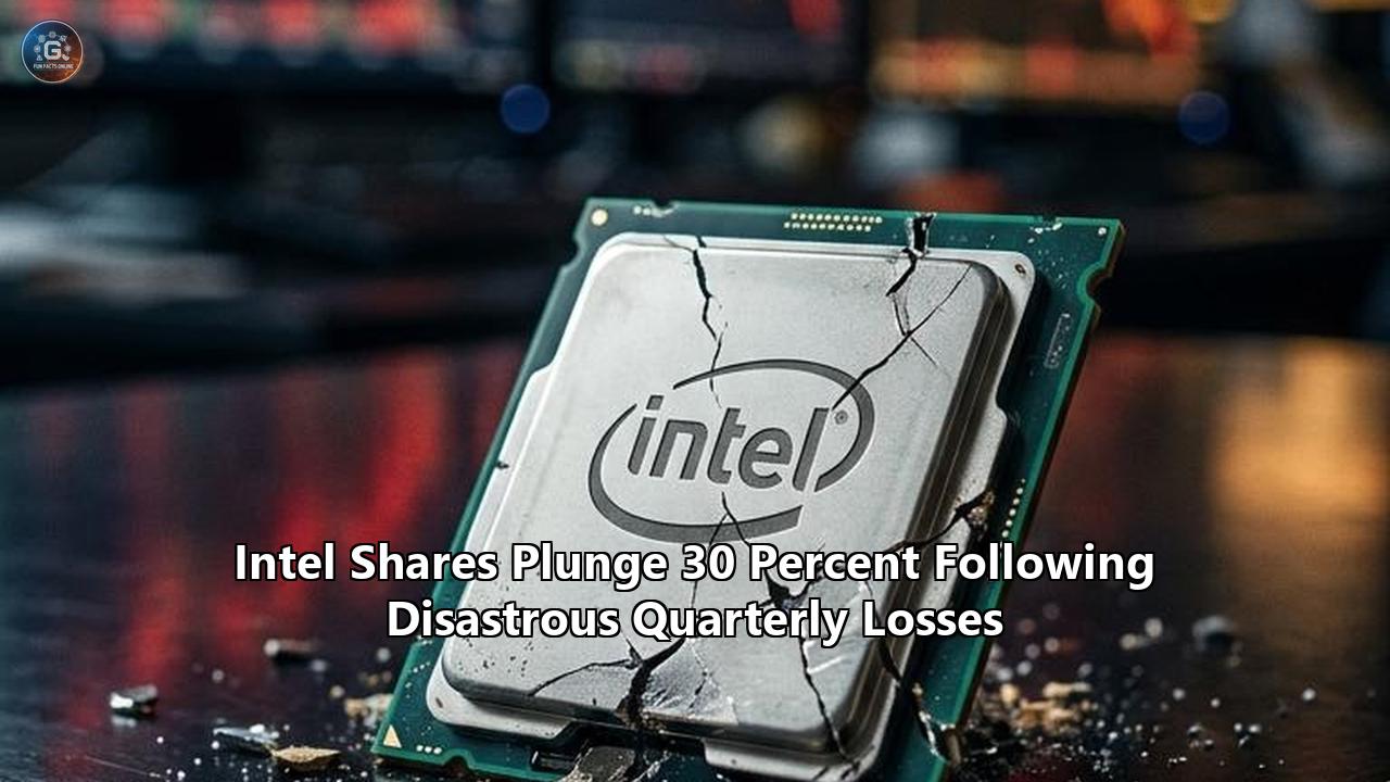
Wall Street opened to a financial bloodbath as shares of Intel Corporation plummeted nearly 30 percent intraday, culminating in a historic single-day collapse that erased more than $32 billion in market capitalization. The rout, sparked by a disastrous second-quarter earnings report, marked the semiconductor pioneer’s steepest stock decline in fifty years, dragging down global chip indices and sending reverberations through international supply chains.
The numbers released by the Santa Clara chipmaker were bleak. Intel reported a second-quarter GAAP net loss of $1.61 billion on revenue of $12.83 billion, missing analyst expectations and falling far short of the $1.48 billion profit recorded during the same period a year earlier. Compounding the immediate financial damage, management delivered a severely downgraded third-quarter outlook, forecasting revenue between $12.5 billion and $13.5 billion alongside an expected net loss per share.
To stem the accelerating cash burn, Chief Executive Officer Pat Gelsinger unveiled an aggressive emergency austerity package. The company confirmed plans to eliminate more than 15 percent of its workforce—amounting to roughly 15,000 to 17,500 jobs—before the close of the year. Capital expenditures for 2024 were slashed by more than 20 percent, targeted down to $25 billion to $27 billion, with further operational reductions mapped for 2025. Most jarringly for long-term institutional shareholders, Intel suspended its quarterly dividend starting in the fourth quarter, halting a shareholder payout tradition maintained continuously since 1992.
"Our Q2 financial performance was disappointing, even as we hit key product and process technology milestones," Gelsinger stated during the earnings call. In a candid internal memorandum distributed to staff, Gelsinger was even more direct about the structural crisis facing the company: "Our revenues have not grown as expected—and we’ve yet to fully benefit from powerful trends, like AI. Our costs are too high, our margins are too low. We need bolder actions to address both".
The severity of the market reaction was immediate. As institutional investors dumped shares in volumes not witnessed since the 1970s, the Intel stock crash emerged as a defining moment in modern tech history, signaling that the company’s multi-year, multi-billion-dollar effort to restore its manufacturing and technological supremacy had hit a dangerous financial and operational wall.
Behind this catastrophic market repricing lies a complex web of technical miscalculations, semiconductor physics, shifting computing paradigms, and brutal manufacturing economics. Understanding how Silicon Valley’s original heavyweight fell into such acute distress requires unpacking the microscopic mechanics of modern silicon fabrication, the economic traps of running multi-billion-dollar cleanrooms, and the sudden architectural pivot that transformed how data centers consume compute power.
Anatomy of the Collapse: Dissecting the Balance Sheet
The immediate trigger for the selloff was not merely that Intel missed quarterly estimates; it was the revelation of where the losses were accumulating and how rapidly the core business model was deteriorating.
In early 2024, Intel fundamentally altered its financial reporting framework, establishing a formal operational wall between two distinct divisions: Intel Products (which designs and sells client computing, data center, and network chips) and Intel Foundry (the internal manufacturing arm responsible for wafer fabrication, packaging, and third-party customer contracts). This separation was intended to demonstrate operational transparency and simulate the relationship an external foundry like Taiwan Semiconductor Manufacturing Company (TSMC) maintains with fabless designers like Apple or Nvidia.
Instead, the newly visible accounting exposed the severe structural drag of Intel’s fabrication business.
================================================================================
INTEL Q2 2024 FINANCIAL BREAKDOWN (GAAP)
================================================================================
Metric                           Reported Q2 2024     Q2 2023 Comparison
--------------------------------------------------------------------------------
Total Net Revenue                $12.83 Billion       $12.95 Billion (-1%)
GAAP Net Income (Loss)           $(1.61) Billion      $1.48 Billion
Gross Margin (GAAP)              35.4%                35.8% (Historical: ~60%)
Intel Products Revenue           $11.80 Billion       $11.35 Billion (+4%)
  - Products Operating Profit    $2.90 Billion        25% Operating Margin
Intel Foundry Revenue            $4.30 Billion        $4.15 Billion (+4%)
  - Foundry Operating Loss       $(2.80) Billion      Loss expanded significantly
Client Computing Group (CCG)     $7.40 Billion        $6.78 Billion (+9%)
Data Center & AI (DCAI)          $3.00 Billion        $3.16 Billion (-3.5%)
  - DCAI Operating Profit        $0.30 Billion        9.1% Operating Margin
================================================================================
While Intel Products managed an operating profit of $2.9 billion—buoyed primarily by traditional PC processor sales in the Client Computing Group—the Foundry division generated a staggering $2.8 billion operating loss in a single three-month span on revenues of $4.3 billion. Over the preceding eighteen months, Intel Foundry had accumulated well over $10 billion in red ink as it attempted to finance new cleanroom infrastructure, acquire costly equipment, and ramp up early-generation silicon.
The collapse in gross margin tells an equally alarming story. For decades, Intel enjoyed a virtual monopoly in personal computers and enterprise servers, routinely printing gross margins between 60 and 65 percent. That structural pricing power allowed the company to fund monumental research and development budgets out of internal cash flow. In the second quarter of 2024, GAAP gross margin contracted to 35.4 percent.
Chief Financial Officer David Zinsner pointed to several interconnected culprits: the accelerated production ramp of the Core Ultra "Meteor Lake" PC processor, heavy startup costs associated with transitioning silicon wafer capacity to Ireland, and substantial excess capacity charges on legacy process nodes. Because Intel was rushing its AI PC silicon to market to defend laptop shelf space against competing processors, it accepted depressed manufacturing margins to seed the ecosystem.
For income-oriented mutual funds, pension systems, and retail investors, the sudden dividend suspension crossed an unforgivable threshold. Intel had long been treated as a bedrock defensive holding in technology portfolios, paying steady capital distributions while funding its long-range engineering. By cutting the dividend entirely to preserve liquidity, Intel signaled to Wall Street that its cash cushion had evaporated to levels where basic capital solvency had to take precedence over shareholder returns.
The Physics of Failure: How the EUV Miscalculation Trapped Intel
To understand why Intel Foundry loses billions while rival TSMC generates tens of billions in pure profit, one must look past quarterly spreadsheets and examine the atomic-scale physics of semiconductor photolithography.
Semiconductor fabrication is the art of transferring microscopic circuit patterns onto silicon wafers. Wafers are discs of hyper-pure monocrystalline silicon, typically 300 millimeters (about 12 inches) in diameter. Billions of microscopic transistors—electrical switches that toggle between 0 and 1—are built layer upon layer across the wafer through a cyclical sequence of chemical deposition, photoresist coating, light exposure, and acid etching.
The limiting factor in how small transistors can be made is the wavelength of light used by the lithography machine to print those circuit lines. For years, the workhorse of the industry was Deep Ultraviolet (DUV) lithography, which utilizes an argon fluoride (ArF) excimer laser emitting light at a wavelength of 193 nanometers.
LITHOGRAPHY WAVELENGTH SCALE
--------------------------------------------------------------------------------
193nm DUV Laser Light:        [===========================================]
13.5nm EUV Laser Light:       [==]
Silicon Lattice Spacing:      [.] (~0.54nm)
--------------------------------------------------------------------------------
Smaller wavelength allows directly resolving sharper, denser transistor gates.
As the industry pushed transistor density past the 14-nanometer node in the mid-2010s, 193-nanometer light was far too wide to print fine features directly. The industry faced two distinct paths forward:
- Extreme Ultraviolet (EUV) Lithography: Utilize an exotic, experimental light source developed by Dutch equipment maker ASML, which operates at a wavelength of just 13.5 nanometers—more than fourteen times smaller than DUV light.
- Multi-Patterning with DUV: Continue using mature 193-nanometer lasers, but split a single circuit layer into two, three, or four separate exposures (Self-Aligned Double Patterning, or SADP; and Self-Aligned Quad Patterning, or SAQP), etching intricate geometries through overlapping physical masks.
Around 2014, under former CEO Brian Krzanich, Intel made what is widely viewed as the most consequential technical blunder in computing history. Viewing ASML’s early EUV machines as too temperamental, unproven, and financially prohibitive, Intel engineers decided to build their upcoming 10-nanometer process node entirely around complex DUV multi-patterning.
The company attempted to push transistor density scaling by an aggressive factor of 2.7x in a single generation, relying on up to quadruple patterning (SAQP).
The physical reality of quadruple patterning proved catastrophic. Printing a single layer of a chip required exposing the wafer, depositing chemical spacers, etching away material, depositing another spacer, and exposing it again, four times sequentially.
Every single step introduced Edge Placement Errors (EPE)—microscopic misalignments measuring fractions of a nanometer between sequential layers. If one pattern drifted by even the width of three silicon atoms, the entire transistor gate short-circuited or failed to connect to the metal interconnect stack above it.
THE MULTI-PATTERNING DEFECT MULTIPLIER
================================================================================
EUV Approach (Single Exposure):
  Wafer --> [Single 13.5nm Flash] --> Etch --> Complete Layer
  * Defect Probability: Low | Process Steps: Few | Machine Cost: High ($150M+)

DUV Multi-Patterning (SAQP - Quad Exposure):
  Wafer --> [193nm Flash 1] --> Spacer Deposition --> Etch
        --> [193nm Flash 2] --> Spacer Deposition --> Etch
        --> [193nm Flash 3] --> Spacer Deposition --> Etch
        --> [193nm Flash 4] --> Chemical Polish   --> Complete Layer
  * Cumulative Drift & Misalignment (EPE) compound exponentially at each step.
================================================================================
While Intel spent five agonizing years (from 2015 to 2020) wrestling with catastrophic defect rates and broken yields on its 10-nanometer DUV line, TSMC made a diametrically opposed bet. The Taiwanese foundry embraced ASML’s first-generation EUV scanners for its N7+ and N5 nodes.
ASML’s EUV machines generate 13.5-nanometer light by dropping microscopic droplets of molten tin inside a vacuum chamber 50,000 times per second, blasting each droplet twice with an industrial carbon dioxide laser to create a high-temperature plasma that radiates extreme ultraviolet photons. The light is so fragile that air absorbs it instantly, requiring the entire exposure process to take place inside a high-vacuum chamber bouncing light across ultra-flat molybdenum-silicon mirrors.
EUV was extraordinarily difficult to engineer, but once operational, it replaced three or four complex DUV masks with a single, pristine flash of 13.5-nanometer light.
By the time Intel finally abandoned its stubborn multi-patterning efforts and pivoted to EUV under Pat Gelsinger, TSMC had already logged millions of production wafer runs, mastered the operational nuances of the scanners, and captured all the premier chip design contracts in the world—from Apple's iPhone silicon to AMD's Zen processors and Nvidia's accelerators.
Intel’s historical delay meant that every modern node it brought online had to absorb the capital depreciation of legacy equipment while concurrently buying backlogged EUV machinery at record prices. The severe margin compressions seen during the Intel stock crash were the delayed mathematical consequence of that decade-old lithography mistake finally coming due on the balance sheet.
Silicon Economics: Wafer Yields and the Cleanroom Trap
The semiconductor foundry business is ruled by unforgiving manufacturing mathematics. Unlike software companies, where distributing code to an extra million users costs virtually nothing, physical chip manufacturing has extreme upfront capital costs and fixed operating expenses.
A modern advanced semiconductor fabrication facility (a "fab") costs between $15 billion and $20 billion to construct, equip, and certify. Cleanroom floors require vibration-isolated concrete slabs, specialized airflow systems capable of filtering particles down to single-digit nanometers, and massive industrial supplies of ultra-pure water and hazardous specialty gases. Inside, dozens of EUV photolithography machines, priced at upwards of $150 million to $350 million each, depreciate on corporate accounting sheets every single day, whether they are processing silicon or sitting idle.
ANATOMY OF A WAFER COST AND YIELD EQUATION
--------------------------------------------------------------------------------
Processed 300mm Silicon Wafer Cost: $12,000 - $20,000 (Advanced Node)
Potential Chips (Gross Dies) per Wafer: 500

Scenario A (Mature Foundry / 90% Yield):
  - Usable Good Dies: 450
  - Net Cost Per Die: $33.33 (High profitability, wide gross margins)

Scenario B (Struggling Foundry Ramp / 45% Yield):
  - Usable Good Dies: 225
  - Net Cost Per Die: $66.66 (Gross margins eliminated, capital loss)
--------------------------------------------------------------------------------
Depreciation + Low Yield = Immediate Balance Sheet Bleeding
Profitability in a fab is governed by two uncompromising metrics:
1. Wafer Yield
Yield represents the percentage of operational, non-defective semiconductor dies harvested from a single processed wafer. When a process node is immature, random airborne particles, chemical contamination, or physical layer defects might render 60 to 70 percent of the dies on a wafer unusable.
Because the cost of running a wafer through a three-month fabrication cycle is fixed—often between $12,000 and $20,000 per wafer on modern nodes—a low yield causes the cost per usable chip to skyrocket. If a fab achieves an 85 percent yield, the economic profit per chip is immense. If the yield drops to 45 percent, every finished processor carries the embedded manufacturing expense of its dead counterparts on the wafer, destroying profitability.
2. Fab Utilization Rates
Cleanroom tools lose value steadily through depreciation. If an advanced fab runs at 90 percent capacity around the clock, that daily depreciation expense is divided across hundreds of thousands of commercially salable chips. If utilization drops to 65 or 70 percent—because PC demand softens or data center buyers look elsewhere—the massive fixed depreciation costs do not diminish. Instead, they concentrate on fewer finished units, triggering a sharp decline in gross margins.
Intel Foundry got crushed by both sides of this equation simultaneously. As Pat Gelsinger pushed to build out capacity across Oregon, Ireland, Ohio, and Germany, the company was absorbing towering capital depreciation costs.
Yet, because Intel’s next-generation nodes were still traversing their initial yield-learning curves, and because external fabless customers (like Qualcomm, Apple, or Nvidia) were hesitant to commit their multi-billion-dollar production runs to an unproven external foundry, Intel was forced to pay for its own underutilized cleanrooms.
When Intel broke out its foundry results for the first time in 2024, the operational veil was stripped away. Wall Street saw that Intel was essentially running a high-cost internal manufacturing shop that lost billions of dollars every quarter trying to keep up with TSMC’s peerless production cadence.
The AI Divergence: The Seismic Shift from CPU to GPU
The manufacturing crisis collided head-on with an architectural revolution in enterprise computing. For forty years, the Central Processing Unit (CPU) reigned as the absolute brain of the computing universe. Every server rack, enterprise cloud cluster, and personal workstation was designed around the host CPU—a category Intel monopolized with its Xeon brand for decades.
Then came generative artificial intelligence and Large Language Models (LLMs).
ARCHITECTURAL DISPARITY: CPU vs. GPU
================================================================================
Intel Xeon CPU (Latency-Optimized):
  [ Control Logic ] [ L1/L2/L3 Caches ]
  [ Core 1 ] [ Core 2 ] [ Core 3 ] [ Core 4 ] ... [ Up to ~64-128 Large Cores ]
  - Task Profile: Complex sequential instructions, branch prediction, deep OS management.
  - Mathematical Mechanism: Scalar / Low-dimensional Vector processing.

Nvidia Hopper/Blackwell GPU (Throughput-Optimized):
  [ Small Cache ] [ Streaming Multiprocessors ]
  [ 10,000+ Small Parallel Arithmetic Logic Units (ALUs) ]
  - Task Profile: Massively parallel matrix multiplication (Tensors).
  - Mathematical Mechanism: High-throughput FP16, FP8, FP4 Floating-Point Math.
================================================================================
A CPU is engineered to be latency-optimized. It features a relatively small number of powerful cores equipped with enormous cache memory, out-of-order execution engines, and speculative branch predictors. Its primary objective is to execute complex, sequential streams of disparate instructions as fast as humanly possible. A CPU excels at running operating systems, database queries, and varied business logic.
In contrast, training and running an AI model does not involve navigating unpredictable code branches. Instead, it requires performing trillions upon trillions of straightforward mathematical calculations—specifically, matrix multiplications and dot products—simultaneously.
For this task, a Graphics Processing Unit (GPU) or dedicated AI accelerator is orders of magnitude more efficient. A GPU features thousands of smaller, simpler arithmetic logic units (ALUs) that crunch identical mathematical operations across vast arrays of numbers in parallel.
When OpenAI demonstrated the commercial power of generative models with ChatGPT, enterprise capital spending shifted overnight. Cloud hyperscalers—Microsoft, Amazon Web Services, Google Cloud, and Meta—did not expand their data center infrastructure budgets by hundreds of billions of dollars in a linear fashion. Instead, they aggressively cannibalized their traditional server budgets.
ENTERPRISE DATA CENTER CAPITAL ALLOCATION SHIFT
--------------------------------------------------------------------------------
Traditional Server Architecture (Pre-2022):
  [ Motherboard: Dual Intel Xeon CPUs ($10,000) ] ===> Captures 70-80% of node cost.

Modern AI Training Server (Post-2023):
  [ 8x Nvidia H100/B200 GPUs ($300,000+) ]       ===> Captures 85-90% of node cost.
  [ Host CPUs (Intel or AMD) ($10,000) ]         ===> Demoted to peripheral manager.
--------------------------------------------------------------------------------
In a traditional enterprise server, dual Intel Xeon processors accounted for the lion’s share of the system's electronic component value. In an AI server cluster, eight Nvidia H100 or Blackwell GPUs can cost well over $300,000, while the host CPUs acting as baseline platform controllers represent a tiny financial footnote.
Intel found itself structurally unequipped to capitalize on this spending shift. Its enterprise data center sales stalled, with the Data Center and AI (DCAI) group posting flat year-over-year revenue of $3.0 billion while generating an operating margin of just 9.1 percent—an almost negligible return for a division that once sustained Intel's corporate empire.
Meanwhile, Nvidia posted record-breaking quarters with triple-digit revenue expansion, pulling in tens of billions in pure profit from the exact hyperscalers whose purchasing dollars once flowed directly to Intel.
Intel tried to counter with its own custom AI accelerator line, the Gaudi series (Gaudi 2 and Gaudi 3). While Gaudi 3 offered competitive raw hardware performance per dollar on paper, it ran into an insurmountable barrier: software ecosystem lock-in.
For nearly two decades, Nvidia had systematically built CUDA (Compute Unified Device Architecture), a proprietary software framework that allows developers to write parallel software code directly for Nvidia hardware. Over fifteen years, every major AI library, optimization algorithm, neural network architecture, and research framework—from PyTorch to TensorFlow—was written, tested, and optimized natively for CUDA.
Software engineers refused to switch to Intel’s open-source software stack, oneAPI, because porting multi-billion-parameter neural networks across unproven compilers created unacceptable technical bugs, latency penalties, and operational downtime. Hardware without a dominant software layer is inert silicon; Intel’s Gaudi ramped far too slowly to plug the multi-billion-dollar hole left by the CPU collapse.
Instruction Set Wars: x86 Under Siege from ARM and AMD
Even within Intel’s traditional fortress—the CPU market—its core technological moat was being breached from two distinct vectors: the rapid rise of the ARM architecture and the technological resurgence of Advanced Micro Devices (AMD).
For more than four decades, the computing landscape was defined by the x86 instruction set architecture (ISA), an intellectual property foundation co-owned primarily by Intel and AMD. The instruction set is the basic vocabulary of a microprocessor—the defined machine instructions that dictate how software commands talk to the silicon gates.
THE ARCHITECTURAL DIVERGENCE: x86 CISC VS. ARM RISC
================================================================================
x86 Architecture (Complex Instruction Set Computer - CISC):
  - Instructions: Variable length, variable complexity.
  - Silicon Overhead: Extensive hardware decode logic required to break complex
    instructions into internal micro-operations (uOps) before execution.
  - Strength: Massive legacy software compatibility across 40 years of computing.
  - Weakness: Higher power consumption, structural thermal overhead.

ARM Architecture (Reduced Instruction Set Computer - RISC):
  - Instructions: Fixed length, simplified operations.
  - Silicon Overhead: Minimal decode logic. Instructions execute cleanly and directly.
  - Strength: Exceptional energy efficiency, high performance per watt.
  - Weakness: Historical lack of native enterprise desktop and server applications.
================================================================================
Historically, the x86 instruction set’s massive software compatibility advantage made it untouchable. Millions of enterprise operating systems, corporate databases, and consumer programs were compiled specifically for x86.
That structural moat began to evaporate in 2020 when Apple cut ties with Intel, ditching x86 processors across its entire Mac line in favor of its custom, ARM-based Apple Silicon (M-series processors). Apple demonstrated that by pairing the clean, efficient Reduced Instruction Set Computer (RISC) design of ARM with advanced silicon packaging and TSMC's cutting-edge nodes, it could deliver laptop chips that outperformed Intel's finest processors while consuming a fraction of the electrical power and generating almost no heat.
The threat quickly spread beyond consumer laptops:
1. Cloud Hyperscalers Build Custom ARM Silicon
Major cloud providers realized that electricity and thermal cooling were their largest operating expenses. Pushing massive x86 processors at high thermal design powers (TDP) was economically inefficient.
Amazon Web Services developed its own proprietary ARM-based server chips, dubbed Graviton, offering cloud compute instances at a 20 to 40 percent discount compared to traditional Intel Xeon instances. Google followed suit with its custom ARM-based Axion processors, while Microsoft deployed Cobalt in its Azure data centers. With every hyperscaler deploying custom internal ARM chips, millions of high-margin server sockets that historically went to Intel vanished permanently.
2. The Windows on ARM Resurgence
In mid-2024, Qualcomm launched its Snapdragon X Elite processors, bringing high-performance ARM-based computing to the Windows client ecosystem. Armed with dedicated Neural Processing Units (NPUs) and impressive battery endurance, Qualcomm broke Intel's near-monopolistic grip on mainstream corporate and consumer laptops, introducing direct pricing competition into Intel's most reliable revenue engine: the Client Computing Group.
3. AMD’s Chiplet Revolution
Simultaneously, AMD pursued an aggressive offensive under the leadership of CEO Lisa Su. Decades earlier, AMD had spun off its capital-intensive manufacturing facilities (which became GlobalFoundries) to operate as a nimble, fabless design firm.
Freed from the multi-billion-dollar burden of building cleanrooms, AMD tapped TSMC’s state-of-the-art fabs to produce its processors. Rather than manufacturing one enormous, expensive monolithic piece of silicon, AMD pioneered a chiplet design architecture.
AMD fabricated small, identical 8-core CPU dies (Core Complex Dies, or CCDs) with near-perfect manufacturing yields, then stitched multiple CCDs together around a central input/output (I/O) die on an advanced substrate package.
MONOLITHIC DIE (HISTORICAL INTEL) VS. CHIPLET ARCHITECTURE (AMD)
--------------------------------------------------------------------------------
Intel Monolithic Die:
  [ Core | Core | Core | Core | Cache | PCIe Controller | Memory Controller ]
  - Single massive silicon block. If one transistor shorts, the entire die is scrap.
  - Wafer yield curve: Low yields on large die footprints; high unit cost.

AMD Modular Chiplets:
  [ Compute Die 1 (8 cores) ]  [ Compute Die 2 (8 cores) ]
  [ Compute Die 3 (8 cores) ]  [ Compute Die 4 (8 cores) ]
                   \              /
             [ Central I/O Controller Die ]
  - Small, modular compute dies produce near 90%+ yields at TSMC.
  - Easy to scale: Mix and match dies to build 8-core laptops or 96-core servers.
--------------------------------------------------------------------------------
With this modular approach, AMD’s EPYC server chips achieved staggering core counts (up to 96 and 128 cores per socket) with superior energy efficiency, steadily capturing market share from Intel’s Xeon processors in corporate data centers. Intel’s historical response—relying on massive, monolithic dies that were expensive to manufacture and generated heavy heat—left the company vulnerable to market share erosion in its most profitable segments.
The Packaging Dilemma and the Irony of Outsourcing to TSMC
By 2024, Intel was caught in a painful logistical bind that exposed the limits of its internal manufacturing. To remain competitive with AMD and Apple, Intel had to abandon pure monolithic designs and transition to its own modular, disaggregated architectures, introduced in client chips like Meteor Lake (Core Ultra Series 1) and Lunar Lake (Core Ultra Series 2).
Instead of printing every component of the processor on a single slice of silicon, Intel split the chip into four discrete tiles:
- Compute Tile: Houses the high-performance CPU cores.
- Graphics Tile: Contains the integrated GPU execution units.
- SoC (System-on-Chip) Tile: Manages memory controllers, AI neural processing units, and power management.
- I/O Tile: Handles high-speed connectivity interfaces like PCIe lanes and Thunderbolt ports.
To link these disparate tiles together, Intel relied on its proprietary advanced packaging technologies, known as Foveros and EMIB (Embedded Multi-die Interconnect Bridge). Foveros allows different silicon tiles to be stacked directly on top of a passive base die in three dimensions, using microscopic copper micro-bumps to bridge electrical connections with minimal latency and high bandwidth.
INTEL DISAGGREGATED TILE PACKAGING (LUNAR LAKE / METEOR LAKE)
================================================================================
             [ Compute Tile ]   [ Graphics Tile ]   [ SoC Tile ]
                    |                  |                 |
             -------------------------------------------------
             [               Foveros 3D Base Die             ]
             -------------------------------------------------
                                     |
             [             Packaging Substrate               ]
================================================================================
Critical Irony:
Intel was forced to pay TSMC to manufacture the high-performance Compute and
Graphics Tiles on TSMC's advanced 3nm (N3B) node, while Intel's internal fabs
handled base-level manufacturing and assembly.
Herein lay the strategic humiliation that crushed Intel’s second-quarter profit margins: Intel did not possess the internal node capability to manufacture the primary compute tiles for its premier client chips.
For both Meteor Lake’s graphics tile and virtually the entire silicon suite of its flagship Lunar Lake processor, Intel had to outsource manufacturing to TSMC, contracting capacity on TSMC’s premium 3-nanometer (N3B) process node.
This operational reality created a devastating financial squeeze:
- Paying Competitor Margins: Intel had to pay TSMC’s rich commercial foundry prices, effectively transferring a chunk of its potential profit margins to its chief manufacturing rival.
- Double Capital Burden: While spending billions to buy external wafers from TSMC, Intel was simultaneously paying billions in depreciation and maintenance expenses on its internal, underutilized cleanrooms in Oregon and Ireland.
- Complex Supply Chains: Shipping raw wafers from Taiwan to packaging plants in Malaysia, Costa Rica, or New Mexico introduced logistical friction, packaging yield overhead, and inventory lag.
This dynamic reached a breaking point in the second-quarter report. Management acknowledged that the accelerated production rollout of its AI PC line had severely dented corporate gross margins. Intel was burning cash to build chips whose most valuable silicon components it could not even manufacture on its own production lines. The market saw this as an undeniable admission that Intel’s internal foundry was falling behind commercial market standards.
The IDM 2.0 Gamble: Five Nodes in Four Years
When Pat Gelsinger returned to helm Intel in early 2021, he diagnosed these structural issues and launched a high-stakes, capital-intensive turnaround program branded as IDM 2.0 (Integrated Device Manufacturing 2.0).
The core thesis was audacious: Intel would not surrender manufacturing like AMD did. Instead, it would double down, spending over $100 billion to rebuild its process capabilities, regain the global transistor performance crown, and open up its cleanroom doors to act as a commercial foundry for third-party chip designers.
To leapfrog TSMC, Gelsinger committed the company to execute an unprecedented engineering roadmap: "Five Nodes in Four Years."
INTEL'S "FIVE NODES IN FOUR YEARS" TECHNICAL ROADMAP
================================================================================
Node Name       Key Technical Innovation              Status / Execution
--------------------------------------------------------------------------------
Intel 7         Enhanced FinFET, 10nm Refinement      Shipped in Alder/Raptor Lake
Intel 4         First Intel EUV Adoption              Shipped in Meteor Lake
Intel 3         High-Density FinFET, EUV optimization Shipped in Xeon 6 Server
Intel 20A       RibbonFET (GAA) + PowerVia (BSPDN)    Internal learning node (Cancelled)
Intel 18A       Refined 1.8nm scale, High-NA ready    Critical target node (2025/2026)
================================================================================
Historically, developing and qualifying a single bleeding-edge semiconductor process node takes an entire fab ecosystem between two and three years of painstaking yield tuning. Attempting to compress five successive generational transitions into a forty-eight-month window required burning extraordinary amounts of capital while operating multiple development fabs simultaneously.
The finish line of this sprint rested on two transformative hardware innovations slated for the sub-2-nanometer era:
1. RibbonFET (Gate-All-Around Transistors)
For more than a decade, the semiconductor industry relied on FinFET (Fin Field-Effect Transistor) architecture, where a 3D silicon "fin" stands upright, wrapped on three sides by the conducting gate.
As transistor gates shrink past 2 nanometers, FinFETs suffer from severe quantum mechanical issues: electrons spontaneously tunnel through the channel even when the transistor is switched "off," causing power leakage, thermal buildup, and signal noise.
FinFET (Three-Sided Gate) vs. RibbonFET / GAA (Four-Sided Gate)
--------------------------------------------------------------------------------
FinFET:                              RibbonFET (Gate-All-Around):
        [ Gate ]                                [ Gate Material ]
      +---+  |  +---+                        =======================
      | S | [Fin] | D |                      --- [ Silicon Nanosheet ] ---
      +---+  |  +---+                        =======================
         [Substrate]                         --- [ Silicon Nanosheet ] ---
                                             =======================
                                             --- [ Silicon Nanosheet ] ---
                                             =======================
(Gate touches fin on 3 sides)         (Gate wraps entirely around each sheet,
                                      eliminating parasitic current leakage)
--------------------------------------------------------------------------------
Intel’s RibbonFET replaces the vertical fin with multiple ultra-thin, horizontally stacked silicon nanosheets (or "ribbons"). The conductive gate material is deposited so that it completely encases all four sides of each ribbon. This Gate-All-Around (GAA) geometry gives the gate total electrostatic control over the conduction channel, preventing current leakage at near-atomic scales.
2. PowerVia (Backside Power Delivery)
In traditional chip manufacturing, both data signal wires and electrical power delivery lines are squeezed together into a complex metal interconnect stack layered on top of the silicon transistors. As transistors shrank, these metal wires became vanishingly thin, creating severe electrical resistance, thermal throttling, and signal crosstalk (RC delay).
Intel’s PowerVia technology flips the architecture upside down. Signal wires remain on the front side of the silicon, while the thick, high-voltage power delivery traces are moved to the backside of the wafer.
To achieve this, the wafer must be flipped, mechanically polished down to a thickness of just a few micrometers using chemical mechanical planarization (CMP), and etched with microscopic nano-Through-Silicon Vias (TSVs) that connect the power grid directly to the underside of the transistors.
PowerVia unclutters the front side of the die, enabling a 30 percent boost in transistor routing density, eliminating power drops, and letting chip designers run processors at higher clock frequencies with improved electrical efficiency.
While RibbonFET and PowerVia represent legitimate masterclasses in semiconductor engineering, developing them simultaneously cost billions of dollars. In the second quarter of 2024, the operational bill for this technological sprint crashed headlong into cooling corporate revenues.
Intel had to fund this monumental R&D roadmap while its server CPU profits were shrinking, forcing management to accept the severe operational cash drain that triggered the Intel stock crash.
Geopolitical Stakes: The CHIPS Act and National Security
The fallout from Intel’s disastrous quarter spread far beyond Wall Street trading floors, sending alarm bells ringing through the halls of government in Washington, D.C.
For the United States, Intel is not just another publicly traded technology company; it is a critical instrument of national security. Intel is the sole American-headquartered corporation capable of designing and fabricating cutting-edge logic chips on domestic soil.
The modern global economy runs on advanced semiconductors. Guided missiles, satellite communications, fighter jets, high-performance computing clusters, banking mainframes, and consumer hardware all depend on advanced silicon nodes.
Yet, over three decades of globalization, the physical manufacturing of advanced microelectronics migrated almost exclusively to East Asia. Today, TSMC fabricates more than 90 percent of the world’s most advanced processors on an island located just one hundred miles off the coast of mainland China.
GLOBAL ADVANCED LOGIC SEMICONDUCTOR MANUFACTURING CONCENTRATION
--------------------------------------------------------------------------------
Taiwan (TSMC):                [=========================================] ~90%
South Korea (Samsung):        [====] ~8%
United States (Intel):        [=] ~2%
--------------------------------------------------------------------------------
Geopolitical Risk: A naval blockade or military conflict in the Taiwan Strait
could instantly halt global production of high-end compute engines.
Recognizing this acute supply-chain vulnerability, the U.S. Congress passed the bipartisan CHIPS and Science Act in 2022, allocating $52.7 billion in direct subsidies and billions more in loans to reshore semiconductor manufacturing to American soil.
Intel emerged as the centerpiece of this industrial strategy. In early 2024, the White House awarded Intel up to $8.5 billion in direct grant funding, coupled with $11 billion in low-interest federal loans and significant investment tax credits, to anchor mega-fab developments in Ohio, Arizona, Oregon, and New Mexico.
Ohio was envisioned as the "Silicon Heartland"—a multi-phase, $28 billion industrial development near Columbus designed to house two advanced fabrication cleanrooms.
However, the disastrous financial figures exposed a fundamental limit of federal industrial policy: government subsidies cannot solve a broken operational business model.
Federal grants under the CHIPS Act are not lump-sum checks deposited into corporate checking accounts on day one. They are structured as milestone-based reimbursements. To unlock the federal funds, Intel must hit specific operational targets: pouring concrete foundations, installing cleanroom equipment, qualifying production lines, and proving commercial viability.
When Intel slashed capital expenditures by 20 percent and announced 15,000 layoffs, it triggered immediate political scrutiny in Washington. Lawmakers questioned why billions in taxpayer subsidies were being steered toward a corporation engaged in massive workforce reductions, while Intel’s management quietly signaled that construction timelines on its flagship Ohio mega-fab would be pushed back toward 2027 or 2028 to match market demand realities.
The geopolitical dilemma is stark: If Intel’s commercial foundry cannot attract profitable third-party customers, American taxpayers cannot realistically subsidize its multibillion-dollar fab expansions indefinitely. A commercially unviable foundry creates a persistent national security liability, leaving the Western world dependent on TSMC’s Taiwanese cleanrooms despite Washington’s best legislative efforts.
Market Repercussions: Takeover Whispers and Leadership Shifts
The violent share repricing following the quarterly report fundamentally altered Intel’s corporate standing on Wall Street.
With the stock plummeting below $22 per share in the immediate aftermath of the earnings release, Intel’s market capitalization fell under $90 billion. For context, at that valuation, the entire company—including its patents, cleanroom facilities, global campuses, and intellectual property—was valued at less than half of AMD's market cap, a small fraction of Broadcom's, and roughly 3 percent of Nvidia's towering valuation.
This collapse pushed Intel's price-to-book ratio down to levels not seen in the technology sector since the 2008 financial crisis. The company became an immediate target for opportunistic corporate suitors and private equity financiers:
- Qualcomm's Approach: Wall Street was stunned by reports that mobile chip giant Qualcomm—a fabless firm that abandoned internal manufacturing decades ago—had explored a potential full or partial acquisition of Intel. While antitrust hurdles across the U.S., Europe, and China made an outright merger improbable, the mere existence of the talks revealed how deeply Intel’s defensive perimeter had crumbled.
- Asset Sales and Restructuring: Pressure surged to spin off non-essential business units. Intel took steps to establish Altera (its programmable logic chip division, acquired for $16.7 billion in 2015) as an independent business looking for private equity investment ahead of an initial public offering. Similar evaluations were directed at Mobileye, its autonomous driving affiliate.
- Private Equity Injections: Financial powerhouses like Apollo Global Management stepped in with creative structured financing, including a $11 billion joint-venture transaction to buy a 49 percent equity stake in Intel’s Fab 34 facility in Leixlip, Ireland, providing cash to fund equipment purchases in exchange for guaranteed future manufacturing returns.
The strategic debate inside the boardroom reached a boiling point over the future of the Foundry model itself.
Wall Street analysts increasingly argued that Intel should follow AMD’s playbook: abandon the foundry entirely, separate into two independent companies, and let a standalone fabless "Intel Products" design competitive processors manufactured entirely at TSMC.
Gelsinger resisted this split, maintaining that without internal fabs, America’s technological sovereignty would be compromised, and Intel would be left with no unique manufacturing edge.
The immense pressure ultimately took its toll at the highest executive level. Just four months after the second-quarter market rout, Intel’s board of directors forced an abrupt leadership transition. On December 1, 2024, Pat Gelsinger retired under board pressure, ending his nearly four-decade association with the company.
The board installed Chief Financial Officer David Zinsner and Michelle Johnston Holthaus (head of Intel Products) as interim co-CEOs while initiating a global search for a successor, formally elevating the products division to the absolute center of corporate decision-making.
The leadership upheaval served as the ultimate confirmation of Wall Street's verdict. The aggressive capital-allocation strategy pursued since 2021 had run out of time and cash before the technical milestones could yield sustainable profits on the bottom line.
Critical Milestones Ahead: The Road to Redemption or Fracture
Intel stands at an existential crossroads. Navigating out of the shadow of its historic financial collapse requires executing several clear, near-term operational and technical milestones:
1. The Commercial Ramping of Intel 18A
Intel's long-term survival hinges on its Intel 18A (1.8-nanometer equivalent) process node. The company has formally achieved basic power-on milestones for its initial internal 18A products: Panther Lake (for client consumer PCs) and Clearwater Forest (for enterprise data center servers).
THE CRITICAL ROADMAP: PROVE 18A OR FACE FOUNDRY SPIN-OFF
================================================================================
Phase 1: Internal Silicon Proof (2025)
  - Successfully ramp Panther Lake (Client) and Clearwater Forest (Server).
  - Prove that RibbonFET (GAA) and PowerVia achieve industry-leading yields.
  - Eliminate the need to outsource primary compute tiles to TSMC.

Phase 2: External Commercial Qualification (2025-2026)
  - Secure binding high-volume wafer commitments from major fabless giants
    (e.g., Apple, Nvidia, Qualcomm, Amazon, Microsoft).
  - Transition Intel Foundry from an internal accounting unit into a standalone,
    commercially disciplined merchant foundry.
================================================================================
If 18A launches on schedule with high manufacturing yields, Intel will regain process density parity—or even a temporary technical lead—over TSMC's competing 2-nanometer (N2) node. This would allow Intel to pull its high-volume client compute tiles back to internal factories, immediately lifting gross margins.
If 18A encounters yield bottlenecks, defect spikes, or thermal delays, Intel will have burned its remaining financial reserves, almost certainly forcing the board to permanently shutter or spin off the foundry division.
2. Signing Anchor External Foundry Customers
Intel Foundry cannot survive solely on Intel's internal product volume. A modern foundry requires a massive, continuous river of external silicon orders to fund the development of successive process nodes.
While Intel announced small packaging and design partnerships with Microsoft and Amazon Web Services, it has yet to land a tier-one consumer silicon giant for high-volume wafer fabrication. Fabless chipmakers remain cautious; they are reluctant to hand their proprietary designs to a company whose products division competes directly with them in the open market.
Intel must prove that its operational firewall is impenetrable and that its foundry team can provide reliable software design kits (PDKs), standard cell libraries, and on-time wafer deliveries.
3. Rebuilding the Data Center and AI Portfolio
Intel cannot afford to sit on the sidelines of the enterprise compute transformation. The company must successfully transition enterprise servers to its high-core-count Xeon 6 processor family (built using both performance cores and energy-efficient cores) to halt AMD's market share momentum.
Simultaneously, Intel needs to clarify its long-term AI hardware roadmap. With the Gaudi series struggling to dent Nvidia’s enterprise dominance, Intel must deliver unified GPU/accelerator architectures that integrate seamlessly with open software ecosystems, offering enterprises a cost-effective alternative for AI inference workloads.
KEY METRICS TO WATCH
--------------------------------------------------------------------------------
* GAAP Gross Margin: Must climb back from ~35% toward the 45-50% range.
* Foundry Operating Losses: Must show steady contraction from $(2.8B) quarterly run rates.
* Intel 18A Defect Density (D0): Must decline below 0.5 defects per square centimeter.
* Third-Party Foundry Revenue: External wafer revenue must move past pilot programs.
--------------------------------------------------------------------------------
The story behind the Intel stock crash is ultimately an object lesson in the uncompromising nature of semiconductor physics and capital allocation. In the microelectronics industry, strategic errors do not show up overnight; they incubate silently inside cleanrooms for years before surfacing with devastating financial momentum.
Intel’s historical reluctance to embrace EUV lithography, combined with its delayed response to the GPU-driven AI boom and the steady rise of the ARM architecture, created a deep operational deficit that the market ruthlessly punished.
The company now faces an unforgiving technical countdown. Whether Silicon Valley's foundational chipmaker emerges from this crisis as a revitalized manufacturing power or fragments into an ordinary fabless design shop will be decided not by corporate rhetoric, but by the relentless physics of the silicon wafers emerging from its cleanroom furnaces over the months to come.
Reference:
- https://investingnews.com/intel-shareholder-lawsuit/
- https://www.forbes.com/sites/roberthart/2024/08/02/intels-29-nosedive-leads-massive-global-chip-stock-selloff-as-ai-hype-sours/
- https://financefeeds.com/intel-stock-30-percent-past-1974-record/
- https://www.scmp.com/tech/big-tech/article/3272888/intel-cut-15-jobs-suspend-dividend-turnaround-push-shares-plummet
- https://www.tomshardware.com/pc-components/cpus/intel-loses-dollar16-billion-as-data-center-cpus-and-foundry-struggles
- https://www.fastcompany.com/91166920/why-are-ai-chip-stocks-down-nvidia-tsmc-arm-intel-layoffs-q2-2024-earnings
- https://www.intc.com/news-events/press-releases/detail/1704/intel-reports-second-quarter-2024-financial-results?utm_source=chatgpt.com
- https://www.architecting.it/blog/intel-q2fy2024-financials/
- https://quartr.com/events/intel-intc-q2-2024_3sbEYaXB
- https://www.foxbusiness.com/markets/intel-shares-sink-15-workforce-getting-axed-suspends-dividend
- https://marklapedus.substack.com/p/intel-posts-results-losses-mount
- https://www.theguardian.com/technology/2024/dec/02/intel-ceo-pat-gelsinger
- https://www.cbsnews.com/news/intel-pat-gelsinger-retires-zinsner-johnston-holthaus-ceo/
- https://www.intel.com/content/www/us/en/newsroom/news/intel-ceo-news-dec-2024.html
- https://english.cw.com.tw/article/article.action?id=3852