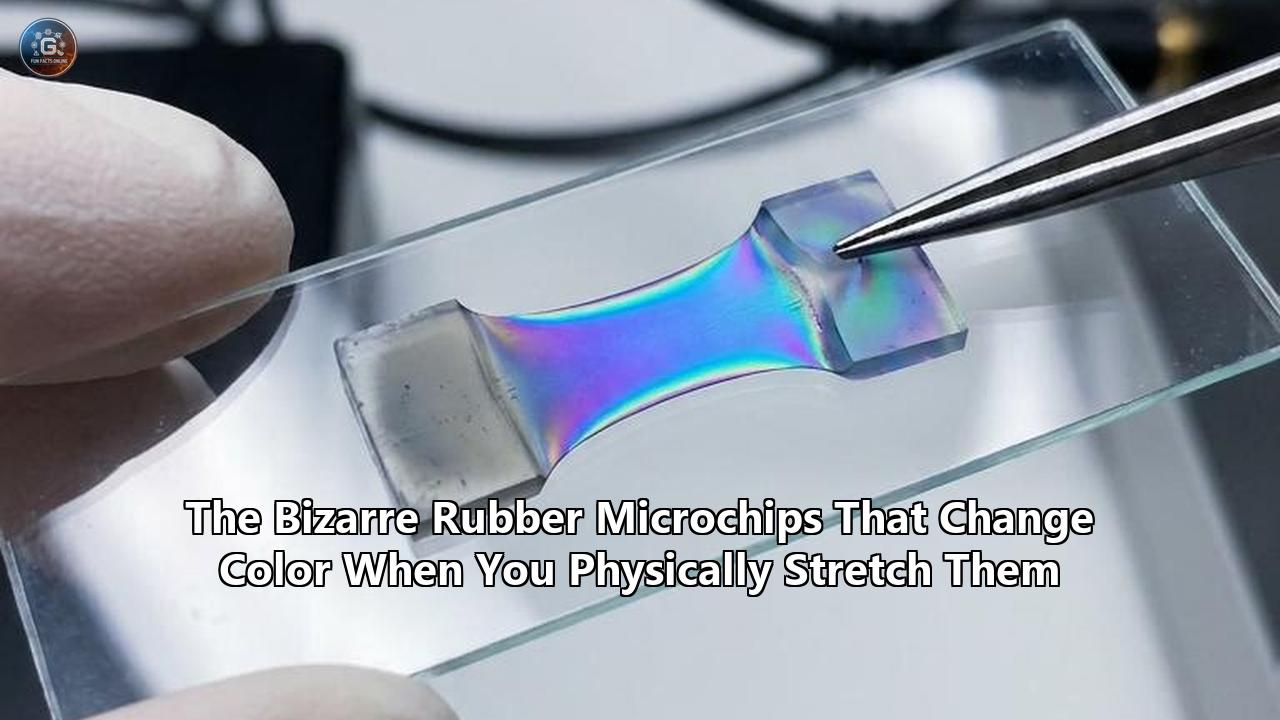
An engineering team at the Pohang University of Science and Technology (POSTECH) has finalized a functional class of photonic devices that shift color across the entire visible spectrum the moment they are physically manipulated. By fusing chiral liquid crystal elastomers (CLCEs) with highly responsive dielectric elastomer actuators (DEAs), the researchers have successfully produced stretchable rubber microchips capable of bidirectional, omnidirectional wavelength tuning without relying on a single drop of chemical dye or pigment.
The breakthrough resolves a fundamental limitation in nano-optics and flexible electronics. Until now, flexible color-shifting materials could typically only be tuned in one direction—usually shifting from longer red wavelengths to shorter blue wavelengths as the material was stretched and its internal microscopic structures compressed. Reversing that shift from blue back to red dynamically under electrical control was considered a massive hurdle in material science. The POSTECH team, led by Professor Su Seok Choi and PhD candidate Seungmin Nam, optimized an actuator structure that permits precise, instantaneous expansion and contraction, actively controlling structural colors from 450 nanometers (deep blue) to 650 nanometers (crimson red).
This is a stark departure from the rigid silicon wafers that have dictated computing for the last six decades. Instead of passing electrons through brittle microscopic gates, these soft architectures transmit data via photons while simultaneously visualizing their own structural strain through instantaneous color shifts.
"This technology can be applied in displays, optical sensors, optical camouflage, direct optical analogue encryption, biomimetic sensors, and smart wearable devices, among many other applications involving light, color, and further broadband electromagnetic waves beyond the visible band," Choi stated following the publication of the foundational research in Light: Science & Applications.
The Mechanics of Mechanochromism
To understand how a physical stretch produces a vivid color change, one must look at the phenomenon of structural color. Traditional displays and image sensors rely on mixing primary colors—red, green, and blue—through light-emitting diodes or chemical luminescent materials. These are passive, fixed, and highly dependent on ambient lighting to maintain their perceived vibrancy.
Structural color, by contrast, relies on the physical geometry of matter. When light strikes a surface packed with periodic nanostructures, certain wavelengths are amplified through constructive interference, while others are entirely canceled out through destructive interference. This is the exact mechanism that gives morpho butterflies their iridescent blue wings and allows chameleons to seamlessly match their surroundings. The color perceived by the human eye is simply the specific wavelength of light permitted to bounce back from the nanoscopic ridges of the material.
By embedding these nanostructures into elastic matrices, engineers create "mechanochromic" photonic crystals. When the material is at rest, the nanostructures sit at a specific distance from one another, reflecting, for example, a green wavelength. When a physical force stretches the material, the distance between those nanostructures widens or narrows. This alters the refractive index and the physical geometry of the crystal lattice, instantly changing the wavelength of the reflected light.
The POSTECH team utilized Chiral Liquid Crystal Elastomers (CLCEs) as their primary mechanochromic material. CLCEs possess a unique helical molecular structure that acts like a microscopic coiled spring. When left alone, the helix has a specific pitch—the distance it takes for a full rotation of the molecule. Light reflecting off this helical pitch produces a distinct color. When the elastomer is stretched, the helix uncoils slightly, lengthening the pitch and reflecting a longer wavelength of light.
However, pulling a material by hand is imprecise. To integrate this into a functioning processor, the color shift had to be controlled via digital, electrical stimuli. This is where Dielectric Elastomer Actuators (DEAs) enter the architecture. DEAs are essentially soft capacitors. When an electrical voltage is applied across them, electrostatic pressure squeezes the elastomer, causing it to deform in a highly controlled manner. By sandwiching the CLCEs with these DEAs, the researchers created a circuit that physically morphs and changes color the moment a specific electrical current is passed through it, achieving bidirectional tuning across the visible spectrum.
Visualizing the Invisible: The Serpentine Architecture Problem
The integration of stretchable rubber microchips into consumer electronics and medical devices has historically faced a major mechanical bottleneck: the interconnects. While the elastomers themselves can stretch like a rubber band, the actual metallic electrodes and processing units embedded within them often cannot.
To bypass this, engineers rely on "serpentine" structures—wavy, snake-like metallic lines that connect various rigid components within a flexible matrix. When the overall device is stretched, these wavy lines uncoil and straighten out, providing elasticity without snapping the metal.
However, predicting exactly when and where these serpentine structures will fail has been a persistent blind spot. Prior to the recent advancements, researchers could only analyze the deformation of a serpentine structure after it had already suffered physical damage. Engineers had to rely on abstract theoretical simulations or autopsy-style observational data gathered only after a stretching cycle resulted in a broken connection.
The POSTECH team directly solved this by applying their structural color technology to the serpentine interconnects. In findings published in the journal Advanced Science, the researchers demonstrated a system that enables precise, real-time visualization of structural deformation. Because the surrounding CLCE matrix shifts color at the exact site of mechanical stress, engineers can now visually map the distribution of strain across a complex electronic web with their naked eyes.
If a specific curve of a serpentine wire is bearing too much load, the microscopic area immediately surrounding it will shift from blue to yellow, or yellow to red, perfectly correlating with the intensity of the physical strain. This real-time color mapping was heavily validated through theoretical finite element analysis, proving that the optical shift matches the precise electrical field distribution and mechanical stress within the nanomatrix.
The Diagnostic Potential of Multistate Optical Biosensors
The implications for this technology extend far beyond material durability tests. The ability to link a physical or chemical interaction directly to a dramatic, visible color shift is rapidly opening new pathways in medical diagnostics and multianalyte recognition.
A highly cited study published in ACS Nano details how these stretchable photonic crystals can be adapted into complex biological sensors. Researchers developed a stretchable photonic crystal (PC) chip designed specifically for saccharide identification. Saccharides—carbohydrates and sugars—are notoriously difficult to differentiate in low concentrations because their molecular structures are incredibly similar.
The research team discovered that by employing a "multistretch analysis," they could use the stretchable rubber microchips to differentially enhance fluorescence signals across broad spectral regions. When the chip is stretched (with an increased stretch ratio of 0 to 40%), the photonic stopbands shift toward the blue end of the spectrum. This physical shift significantly amplifies the fluorescence of specific chemical complexes applied to the chip.
Using only a single fluorescence complex, the stretchable PC chip successfully discriminated 14 similarly structured saccharides at a microscopic minimum concentration of 10⁻⁷ M. The researchers were able to definitively distinguish between varying concentrations of saccharides in real-world liquid mixtures, including standard beverages and complex biological samples.
This optical amplification eliminates the need for bulky, multi-reagent chemical testing arrays. Instead of a lab technician running a dozen separate chemical assays, a single stretchable chip can be mechanically elongated. As the material stretches and its structural color shifts, it sequentially hits the precise wavelengths necessary to illuminate and identify a dozen different target molecules.
Bridging the Gap: Fiber Circuits and High-Density Soft Computing
The push toward flexible photonics is not occurring in a vacuum. It coincides with massive leaps in alternative, non-rigid computing platforms. In early 2026, a team of Shanghai-based scientists published a landmark paper in Nature detailing the creation of a "fiber chip"—a soft, highly elastic thread that houses large-scale integrated circuits.
Moving entirely away from the flat, two-dimensional architecture of silicon wafers, the Shanghai team built complex electronic networks directly inside flexible, hair-thin fibers utilizing a novel "multilayered spiral architecture". The density of this soft computing thread is staggering: a single one-millimeter section of the fiber can house 10,000 transistors. This is equivalent to the processing power required to run a modern heart pacemaker, entirely contained within a flexible thread that can be woven into standard fabrics.
Durability tests demonstrated that the fiber chip can survive up to 100,000 extreme bend cycles. In one demonstration, the delicate-looking thread maintained total electronic performance even after being run over by a 15.6-ton commercial truck.
When the structural color capabilities of the POSTECH devices are paired with the computational density of these new Shanghai fiber chips, the foundation for entirely autonomous "e-skin" is established. A single piece of flexible fabric could contain the processing power to monitor biometric data, combined with a mechanochromic surface that visually alerts the user to physiological changes.
For example, an interactive electronic fiber sensor utilizing these principles can monitor massive joint movements and minute muscle micro-vibrations simultaneously. Researchers at the University of California successfully integrated a mechanochromic photonic crystal microtubule into an electronic piezoresistive fiber. The resulting sensor featured an optical and electrical response time of just 80 milliseconds and a massive working range, accommodating up to a 200% physical stretch while displaying continuous color changes from 632 nanometers down to 439 nanometers.
This high-resolution interaction—translating invisible physiological strain into an immediate, full-color visual display—promises to fundamentally disrupt athletic performance monitoring, physical rehabilitation, and the integration of brain-computer interfaces within smart clothing.
The Photonic Computing Transition
The development of stretchable structural color microchips is a specialized branch of a much larger transition currently tearing through the global tech sector: the shift from electronics to photonics.
The semiconductor industry is rapidly approaching the physical limits of Moore's Law. Silicon transistors can only be shrunk so far before quantum tunneling effects render them useless, and the sheer heat generated by pushing electrons through microscopic copper wiring is currently bottlenecking the expansion of global artificial intelligence data centers.
Photonic chips bypass these limitations by transmitting data using light (photons) rather than electricity (electrons). Photons do not experience electrical resistance in the same way electrons do, meaning optical circuits generate virtually zero heat and can transmit data at the speed of light, vastly outperforming traditional silicon architecture in both speed and energy efficiency.
The primary barrier to mass adoption has always been the manufacturing complexity and high cost of creating nanoscale optical components. However, capital is aggressively flowing into solutions. In April 2026, the Edinburgh-based hardware firm Cnuic secured $3 million in pre-seed funding to finalize a revolutionary photolithography device designed specifically for the rapid, reconfigurable production of photonic chips.
Backed by Tensor Ventures and Silicon Valley's Blank Space Ventures, Cnuic's prototype enables 3D control over light properties during the manufacturing process, a capability that was previously impossible. The firm claims this technology will enable a new scale of commercial photonic chip production, specifically targeting the bottlenecks in AI model training and data center power consumption.
More crucially, the underlying lithography advancements pursued by companies like Cnuic open the door for the scalable production of metalenses, 3D photonic crystals, and the exact type of flexible optical gratings required to manufacture stretchable rubber microchips en masse. If the optical lithography can be scaled, the cost of producing soft, color-shifting processors will plummet, allowing them to move out of university testing labs and into commercial supply chains.
Controlling Light with Light: The Liquid Crystal Metasurface
While mechanical stretching is a powerful way to alter optical properties, it requires physical space and mechanical actuation. For deeply embedded systems, researchers are developing ways to manipulate the refractive properties of liquid crystals without any physical movement at all.
In April 2026, physicists at the Australian National University (ANU) published research in Nanoscale demonstrating a method for controlling static optical components entirely with light. The ANU team focused on metasurfaces—surface arrays built from nanoscopic shapes smaller than the wavelength of visible light. Metasurfaces are conventionally static; once they are manufactured from a dielectric material like hydrogenated amorphous silicon, their optical properties are locked into place.
To overcome this, the ANU researchers embedded a static metasurface into a bath of nematic liquid crystals mixed with a highly specific photoresponsive dye called methyl red.
"We can change the optical response of the metasurface optically - without any electrodes, magnetic components or heating elements, just using light," explained Dr. Yana Izdebskaya, the project lead and a member of the ARC Centre of Excellence for Transformative Meta-Optical Systems.
Methyl red is a large dye molecule that physically switches between a straight geometry and a bent geometry when illuminated by green light (specifically at a wavelength of 532 nm), depending on the polarization of the incoming light. When a green laser strikes the dye, the molecules snap into a new shape. This localized geometric shift acts like a microscopic lever, shifting the orientation of the surrounding long, skinny nematic liquid crystals.
By forcing the liquid crystals to realign, the refractive index of the medium covering the static metasurface changes instantly. The ANU team utilized a metasurface composed of elliptical silicon nanocylinders designed to create powerful electric and magnetic dipole resonances. By simply changing the polarization of the green control light, the team successfully modulated the strength of the dipole resonances in the infrared spectrum.
This optical switching is entirely reversible, a massive leap forward for dynamic beam shaping and signal processing. By removing the need for physical actuators, electrodes, or heating elements, this liquid crystal metasurface technology provides a direct blueprint for how future stretchable rubber microchips could process incoming data. Instead of relying purely on mechanical strain to dictate their output, these systems could function as highly efficient optical switches, using external light pulses to route data through a flexible matrix.
Aerospace and Heavy Industry: Structural Health Monitoring
Beyond the realm of wearables and biomedical devices, the integration of mechanochromic sensors is poised to overhaul how civil and aerospace engineers monitor structural integrity.
Currently, monitoring the structural health of a commercial airliner wing or a suspension bridge relies on a dispersed network of rigid strain gauges and piezoelectric sensors. These sensors are brittle, require constant power, and only provide localized data exactly where they are mounted. If a micro-fracture develops an inch to the left of a traditional strain gauge, the system will not register the anomaly until the crack propagates to the sensor itself, which is often too late.
Applying a layer of stretchable structural color microchips across critical load-bearing surfaces provides a continuous, zero-power, omni-directional monitoring system. Because the color shift is tied directly to the physical geometry of the photonic crystal, it requires no external electricity to function in a passive monitoring state.
If an airplane wing coated in a mechanochromic polymer is subjected to dangerous levels of aerodynamic flutter, the micro-strain on the aluminum will transfer directly into the flexible coating. Ground crews conducting visual inspections would not need to hook up complex diagnostic equipment; a high-stress zone on the wing would simply appear bright red against a baseline blue background.
Furthermore, because these systems can be highly tuned, engineers can design the photonic crystals to remain invisible (reflecting wavelengths outside the visible spectrum, such as near-infrared) until a specific threshold of stress is breached. At the exact moment the structural load exceeds safety limits, the material would instantly shift into the visible spectrum, creating a high-contrast visual alarm.
The Moiré Effect and Twisted Nano-Crystals
The manipulation of photonic crystals is also occurring at the ultra-compact, on-chip level. While macro-stretching relies on widening the gaps between nanostructures, researchers are utilizing the "moiré effect" to tune light properties without vast physical deformation.
In April 2025, researchers from the Harvard John A. Paulson School of Engineering and Applied Sciences, working alongside teams from Stanford and UC Berkeley, unveiled a new on-chip sensor utilizing twisted moiré photonic crystals.
The moiré effect occurs when two repeating patterns are overlaid slightly off-axis. If you lay two sheets of tightly woven mesh over one another and slightly rotate one, massive, complex secondary patterns emerge as the lines cross. In optics, overlaying two photonic crystal lattices and twisting them by a fraction of a degree drastically alters how light propagates through the structure.
The Harvard team utilized MEMS (Micro-Electromechanical Systems) technology to actively control the twist angle and the vertical distance between the two layers of photonic crystals in real time. Mounted on vertical and rotary actuators, the entire device spans only a few millimeters and is completely CMOS-compatible, meaning it can be mass-fabricated in standard foundry environments.
"Twisted moiré photonic crystals are promising for engineering smaller, more powerful optical systems because they offer highly tunable optical properties, precise light control, compact and scalable design, and broad application potential across various advanced photonic technologies," noted Eric Mazur, the Balkanski Professor of Physics and Applied Physics at Harvard and the senior author of the paper.
By utilizing micro-rotation rather than macro-stretching, the Harvard device can simultaneously detect detailed polarization and wavelength information. While this twisted crystal system is not made of rubber, the underlying principle of physically moving crystal lattices to bend light parallels the exact mechanisms used in flexible mechanochromics. Merging the micro-rotational precision of moiré crystals with the macro-elasticity of CLCEs is currently viewed as a major theoretical target for next-generation optical engineering.
Optical Encryption and Active Camouflage
The precise bidirectional wavelength tuning achieved by the POSTECH team also introduces highly disruptive capabilities in the field of analog optical encryption and active camouflage.
Digital encryption relies on complex mathematics to scramble data, but analog optical encryption utilizes the physical properties of light—polarization, phase, and precise wavelength—to hide information in plain sight. A message or a QR code could be embedded into a flexible photonic matrix. In its resting state, the matrix reflects a uniform structural color, rendering the data invisible.
However, because the POSTECH researchers proved that their CLCE-based photonic device can precisely control structural colors over a broad range of visible wavelengths (450 nm to 650 nm) using electrical stimuli, the material acts as a programmable optical lock. Only when a highly specific, pre-determined electrical voltage is applied to the Dielectric Elastomer Actuators will the matrix deform to the exact geometry required to reveal the hidden optical pattern.
Because the color generation does not rely on mixing traditional RGB light—which can be easily intercepted and digitally reproduced by modern cameras—structural color encryption is highly resistant to standard optical hacking. The intrinsic wavelength of the light itself is the key.
This same principle is the foundation for advanced active camouflage. Current military camouflage relies on static, printed patterns. Active camouflage systems have been attempted using heavy, rigid LCD or OLED panels, which are completely unsuited for combat uniforms or curved vehicular armor. A soft, stretchable matrix that can actively shift its structural color in all directions based on external electrical stimuli allows for true biomimetic camouflage—a synthetic chameleon skin. By utilizing a network of external cameras to sample the ambient environment, an onboard processor could theoretically apply rapid micro-voltages across the DEA layers, continuously morphing the structural color of a soldier's uniform to perfectly match the surrounding foliage or urban rubble.
The Quantum Horizon
As the manufacturing of these optical chips matures, their applications are rapidly colliding with the frontiers of quantum computing. Quantum information processing (QIP) relies on isolated atomic systems acting as nonlinear gates and memory, paired with photons acting as rapid information carriers.
A highly functioning quantum network requires nodes capable of transferring quantum information into photons without disturbing the delicate quantum state. Two-dimensional photonic crystals offer an incredibly controllable electromagnetic environment, perfectly suited for the compact integration and complete isolation of these fragile quantum systems by physically suppressing spontaneous light emission.
In solid-state implementations, researchers embed semiconductor quantum dots (QDs) directly into photonic nano-cavities. These cavities act as the nodes, while the surrounding photonic crystal waveguides act as the physical channels through which the qubits travel. The cavity-waveguide-cavity architecture allows a quantum dot in a source cavity to emit a photon preferentially into the cavity mode, securely transferring the data to a target cavity across the chip.
The primary challenge in mapping atomic qubits to photonic qubits is loss—energy bleeding out into the surrounding environment. The coupling between the quantum dot and the cavity must dramatically outpace any external coupling. This requires absolute, nanoscale precision over the electromagnetic environment.
The introduction of stretchable and tunable photonic crystals introduces an entirely new variable into quantum chip design. If the geometry of the nano-cavity can be actively tuned in real-time by mechanically stretching the matrix, engineers gain the ability to physically tune the resonance of the cavity to perfectly match the emission frequency of the embedded quantum dot. While merging delicate quantum dots with highly flexible rubber matrices remains deeply experimental, the ability to physically manipulate the optical pathways on a quantum chip could resolve some of the most persistent bottlenecks in scalable quantum networking.
The Unresolved Bottlenecks and Future Trajectory
Despite the rapid succession of breakthroughs from late 2024 through early 2026, the transition of this technology from controlled laboratory environments to commercial deployment faces several acute engineering challenges.
The first is thermal stability. While the photonic transmission of data inherently generates less heat than electrical transmission, the flexible polymers that house these systems—specifically Chiral Liquid Crystal Elastomers—are notoriously sensitive to ambient temperature changes. If an aerospace engineer coats an aircraft wing in a mechanochromic polymer, the extreme temperature fluctuations between a sun-baked tarmac and the sub-zero environment at 35,000 feet will cause the elastomer matrix to naturally contract and expand. This thermal deformation directly impacts the periodic nanostructures, potentially causing false color shifts and corrupting the strain data. Researchers are currently attempting to formulate advanced polymer blends that decouple thermal expansion from mechanical strain, ensuring the chip only changes color when subjected to actual physical force.
The second major hurdle is continuous power management for the active, electrically stimulated chips. While the passive sensors require no power, the actively tuned devices driven by Dielectric Elastomer Actuators require high operational voltages to generate the necessary electrostatic pressure. Pushing high voltage through flexible, wearable fabrics introduces obvious safety and battery density limitations. Integrating miniaturized, flexible power sources—such as stretchable supercapacitors or triboelectric nanogenerators that harvest power from the wearer's physical movement—is viewed as the mandatory next step for commercializing active e-skin.
Finally, the mass fabrication of large-area structural color matrices remains difficult. The precise roll-to-roll nano-imprinting required to stamp millions of microscopic ridges into a sheet of rubber is highly susceptible to microscopic defects. A single misalignment in the manufacturing line can disrupt the periodic structure, ruining the photonic stopbands and resulting in dead, colorless zones across the material. The integration of advanced photolithography startups, like Cnuic, alongside established CMOS manufacturing pipelines, will dictate how quickly these yield rates can be improved.
The commercialization timeline hinges on identifying the most viable initial markets. Highly specialized medical diagnostics, such as the single-chip multianalyte saccharide detectors, will likely see the first real-world deployments. The ability to discriminate between complex biological markers at a concentration of 10⁻⁷ M using a single, disposable, stretchable chip offers immediate value to clinical pathology labs looking to cut reagent costs.
Simultaneously, the high-end athletic and physical rehabilitation markets are rapidly prototyping user-interactive electronic fiber sensors. The ability to continuously map large joint movements and track the exact strain on recovering ligaments through an 80-millisecond optical response loop provides a level of biomechanical feedback that rigid accelerometers simply cannot match.
The final phase of adoption will likely be the heaviest: replacing the foundational rigid sensors in global infrastructure and computing architectures. The creation of bidirectional, omnidirectional wavelength tuning within a soft actuator represents a clean break from twentieth-century electronic design. Engineers are no longer constrained to flat boards, rigid wires, and passive pigments. By harnessing the physical geometry of light through flexible, dynamic matrices, the computing platforms of the coming decade will be as soft, responsive, and visually expressive as biological skin. Watch for the upcoming integration of these mechanochromic capabilities specifically within the rapidly expanding field of soft robotics, where tactile feedback and visual state-indication remain critical, unresolved operational requirements.
Reference:
- https://analyticalscience.wiley.com/content/news-do/flexible-stretchable-photonic-device-enables-structural-color-tuning-across-long-and
- https://www.photonics.com/Articles/Flexible-Stretchable-Device-Addresses-Tuning/a70031
- https://www.eurekalert.org/news-releases/1069117
- https://pubs.acs.org/doi/10.1021/acsnano.2c08708
- https://www.youtube.com/watch?v=iMLqjJHKA5I
- https://tech.eu/2026/04/28/cnuic-secures-eur3m-pre-seed-to-unlock-next-generation-photonic-chip-production/
- https://science.anu.edu.au/news-events/news/controlling-light-light-using-dyed-liquid-crystals
- https://spie.org/news/0986-quantum-information-processing-on-photonic-crystal-chips