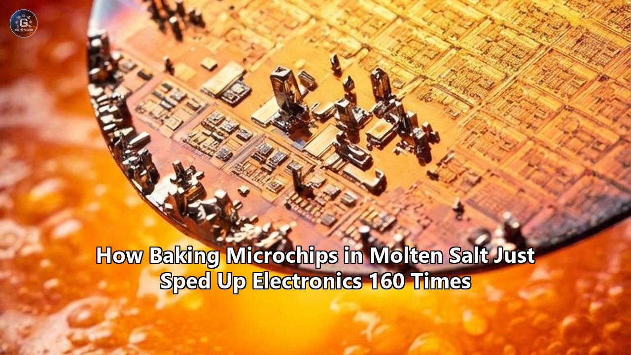
Last week, an international team of researchers operating out of the Helmholtz-Zentrum Dresden-Rossendorf (HZDR) and TU Dresden published data detailing a 160-fold increase in the macroscopic conductivity of a specific class of ultra-thin materials known as MXenes. The enhancement was achieved by completely abandoning standard wet-chemical etching processes, substituting them with a high-temperature technique utilizing molten salts and iodine vapor. This process, designated the GLS method, strips away the chaotic chemical impurities that have bottlenecked MXene performance for the past fifteen years, replacing them with a perfectly ordered atomic structure.
The resulting material, a chlorine-terminated titanium carbide variant (Ti3C2Cl2), not only demonstrated a 160-fold leap in raw electrical conductivity but also exhibited a 13-fold enhancement in terahertz conductivity and a nearly fourfold increase in charge carrier mobility. By bringing atomic-level precision to a material family long plagued by surface disorder, this development alters the trajectory of next-generation hardware, establishing a viable pathway toward faster, more efficient electronic components, advanced energy storage systems, and highly specialized sensors.
The Silicon Ceiling: FinFET, GAA-FET, and the Interconnect Crisis
Contextualizing why a 160-fold conductivity increase in a two-dimensional material represents a critical industry event requires examining the physical limits currently suffocating traditional semiconductor manufacturing. Modern computing relies on billions of silicon-based transistors packed onto individual dies. For decades, the industry adhered to Moore’s Law by continually shrinking the planar transistor. When the planar architecture hit quantum tunneling limits around 2011, the industry pivoted to the 3D FinFET design. As FinFETs reached their electrostatic limits recently at the 3-nanometer and 2-nanometer nodes, fabrication giants transitioned to Gate-All-Around (GAA-FET) nanosheet architectures to maintain control over the current channel.
However, as the transistors themselves continue to evolve and shrink, they are no longer the primary bottleneck restricting processor speeds. The copper interconnects—the nanoscale wiring that links these billions of logic gates together—are failing under the constraints of quantum physics.
As copper wires shrink to a few nanometers in width, their electrical resistance skyrockets. This occurs due to a phenomenon known as surface scattering. The mean free path of an electron traveling through copper at room temperature is roughly 39 nanometers. When the width of the wire is reduced to dimensions smaller than the electron's mean free path, the electron physically bounces off the walls and grain boundaries of the wire. This relentless scattering generates immense electrical resistance and debilitating waste heat.
Furthermore, copper cannot be deposited directly onto silicon; it requires a barrier layer, typically made of tantalum and titanium nitride, to prevent copper atoms from diffusing into the logic gates and short-circuiting the device. At a width of 10 nanometers, these barrier layers consume a massive percentage of the wire's cross-sectional volume, leaving very little room for the actual conductive copper. The semiconductor industry has been actively searching for a 2D material that can conduct electricity efficiently at atomic thicknesses to replace or augment these failing copper interconnects without requiring bulky barrier layers.
Anatomy of a 2D Material: The MXene Profile
MXenes (pronounced "max-eens") have been a prime candidate for this interconnect role since their initial discovery at Drexel University in 2011. They belong to a rapidly expanding family of two-dimensional inorganic compounds made from stacked layers of transition metals—such as titanium, molybdenum, vanadium, or niobium—interleaved with layers of carbon or nitrogen.
These 2D sheets are not grown from scratch; rather, they are synthesized top-down from a bulk parent material called a MAX phase. The crystallography of a MAX phase is highly specific. The 'M' represents the early transition metal, the 'X' stands for the carbon or nitrogen atoms, and the 'A' represents a group of elements, usually aluminum or silicon, which serve as the atomic glue binding the layers together.
The chemical bonds within the M-X layers are a robust mix of covalent, metallic, and ionic bonds, making them incredibly stable and hard. Conversely, the bonds connecting the M-X layers to the 'A' layers are weaker metallic bonds. To create the 2D MXene, chemists exploit this bond discrepancy. They must selectively extract the 'A' layer, dissolving it away to leave behind a free-standing, accordion-like structure of highly conductive transition metal carbide or nitride.
Because their core consists of transition metals, MXenes possess an intrinsic metallic conductivity that many other 2D materials, such as transition metal dichalcogenides (TMDs), fundamentally lack. Furthermore, they are highly hydrophilic, meaning they can be dispersed in water and processed into printable inks, making them highly versatile for large-scale manufacturing. Yet, the physical extraction of that 'A' layer has historically come with a severe structural penalty that crippled their electronic performance.
The Chemical Trap: The Legacy of Hydrofluoric Acid
Until this recent breakthrough at HZDR and TU Dresden, the standard protocol for etching the aluminum 'A' layer out of the MAX phase relied heavily on highly aggressive, hydrofluoric acid (HF)-based solutions. When the solid MAX phase precursor is submerged in an aqueous HF bath, the acid aggressively attacks and dissolves the aluminum layer, pulling it out as aluminum fluoride.
The laws of thermodynamics dictate that the newly exposed transition metal surfaces cannot remain bare. In the highly reactive, water-rich environment of an acid bath, the surface titanium atoms immediately seek to lower their surface energy by bonding with whatever elements are available in the immediate vicinity. As a result, the outer surfaces of the MXene sheets become randomly coated with a disorganized mix of oxygen (O), hydroxyl (OH), and fluorine (F) atoms.
These surface atoms, known as terminations, dictate the fundamental behavior of the material. "They strongly influence how electrons move through the material, how stable it is, and how it interacts with light, heat, and chemical environments," explained Dr. Mahdi Ghorbani-Asl from the Institute of Ion Beam Physics and Materials Research at HZDR. Under the HF etching method, these terminations are scattered chaotically across the lattice. A single nanometer of the surface might feature a highly electronegative fluorine atom, immediately followed by an oxygen atom, and then a hydroxyl group.
The Pothole Effect: How Disorder Kills Conductivity
This random assortment of surface terminations creates a highly uneven, jagged electronic landscape across the atomic sheet. From the perspective of an electron attempting to travel across the 2D plane under an applied voltage, this chemical disorder manifests as a series of erratic, unpredictable electrostatic fields.
Dr. Dongqi Li from TU Dresden characterized the severity of this issue explicitly, noting that "this atomic disorder limits performance because it traps and scatters electrons, much like potholes slowing traffic on a highway".
When an electron encounters a shift in the local electric field caused by a sudden transition from a fluorine termination to a hydroxyl termination, its momentum is disrupted. It scatters off the defect. This scattering drastically reduces the charge carrier mobility—the strict metric defining how fast an electron can move through a semiconductor or conductor under a given electric field. For years, this "pothole" effect has suppressed the real-world conductivity of MXenes, keeping them far below their theoretical performance ceilings and limiting their integration into commercial electronics. Removing these defects via traditional wet chemistry proved physically impossible, as the presence of water inherently forces the creation of hydroxyl and oxygen terminations.
The GLS Molten Salt Alchemy: Engineering Perfect Atomic Order
The research published last week sidesteps the aqueous acid trap entirely by utilizing the GLS method, a technique that operates in a completely different chemical regime. Instead of employing liquid acids at room temperature, the researchers immersed the solid MAX phases in high-temperature molten salts, carefully introducing iodine vapor into the reaction chamber.
Operating at temperatures typically ranging between 550°C and 750°C, the chemical dynamics shift toward Lewis acid-base reactions. In this high-temperature liquid environment, the cations in the molten salt (for example, zinc or copper ions) act as Lewis acids. Because these metallic cations possess a higher redox potential than the aluminum atoms trapped within the MAX phase, a direct redox coupling occurs. The molten salt effectively oxidizes the aluminum, pulling it out of the MAX phase structure and dissolving it into the bath.
Simultaneously, the halogen atoms from the salt—in this case, chlorine—bond directly to the freshly exposed titanium surfaces. Because the environment is strictly controlled, entirely devoid of water, and driven by precise thermodynamic substitution, the chlorine atoms attach in a perfectly uniform grid.
The result is Ti3C2Cl2: a MXene sheet possessing absolute atomic order, entirely free from the chaotic mix of oxygen, fluorine, and hydroxyl groups. Unwanted impurities are effectively eliminated, yielding a pristine surface. The realization of this process opens a direct avenue for the mass production of molten salt microchips, where ultra-pure 2D materials can be reliably manufactured at scale without the debilitating performance penalties inflicted by wet chemistry.
Decoding the 160-Fold Performance Leap
The elimination of surface disorder yielded performance metrics that immediately redefine the material's viability across multiple engineering sectors. By removing the atomic "potholes," the TU Dresden and HZDR team observed a 160-fold increase in macroscopic conductivity compared to identical Ti3C2 material synthesized via the traditional HF etching method.
Macroscopic conductivity refers to the bulk flow of current across the material over relatively large distances, encompassing numerous individual sheets and grain boundaries. A 160-fold multiplier shifts the material from being a moderately effective conductor to a highly competitive metallic interconnect candidate capable of rivaling heavily engineered metals at the nanoscale.
Furthermore, the researchers recorded a nearly fourfold increase in charge carrier mobility. Mobility dictates how quickly a transistor can switch states, and how little voltage is required to push a signal from one sector of a logic board to another. By maximizing mobility, circuits generate significantly less waste heat, require lower input power, and can be clocked at much higher frequencies. High charge carrier mobility is the primary prerequisite for next-generation radio frequency (RF) chips and ultra-fast logic gates.
Dr. Li emphasized the magnitude of this shift, stating, "The results were striking. The chlorine-terminated MXene variant showed a 160-fold increase in macroscopic conductivity and a 13-fold enhancement in terahertz conductivity compared with the same material made by traditional methods. In addition, a nearly fourfold increase in charge carrier mobility was observed, a key measure of how freely electrons move through a material".
Halogen Customization: Tuning the Electromagnetic Spectrum
Beyond raw electron speed, the GLS method provides engineers with an unprecedented level of control over the material's inherent properties. By simply changing the specific type of molten salt used in the crucible, researchers can dictate exactly which halogen atom coats the MXene surface.
The team successfully demonstrated the attachment of chlorine, bromine, and iodine. Because each of these halogens possesses a radically different atomic radius, electronegativity, and electron cloud configuration, swapping them out fundamentally alters the MXene's electronic, optical, and thermal profile.
This behavior allows the material to be tuned to interact with specific wavelengths of light and radiation. For example, the pristine chlorine-terminated variant (Ti3C2Cl2) exhibits strong electromagnetic absorption specifically in the 14 to 18 gigahertz (GHz) range. If a hardware engineer requires absorption or shielding in a different frequency band, they can simply swap the bath to a bromine or iodine-based molten salt to shift the response curve. This degree of modularity is highly sought-after, allowing fabricators to dial in specific electromagnetic responses at the atomic level.
Mixing Halogens for Precision Hardware Engineering
The research team took this modularity further by combining different halide salts within the same molten bath. By doing so, they engineered custom MXenes featuring two or even three different types of surface halogens, distributed in carefully controlled, highly ordered proportions.
This multi-halogen termination strategy allows for the meticulous fine-tuning of the material's work function—the minimum amount of energy required to remove an electron from the surface into a vacuum. In advanced semiconductor design, matching the work function of a metallic interconnect to the semiconductor channel is critical for reducing contact resistance, known as the Schottky barrier.
If the work function is mismatched, electrons face an energy wall when trying to pass from the wire into the transistor, resulting in sluggish performance and thermal losses. The ability to precisely engineer the surface chemistry of these 2D sheets ensures that future molten salt microchips can be custom-tailored at the atomic level to perfectly interface with silicon, silicon carbide, gallium nitride, or other advanced channel materials without imposing arbitrary resistance barriers.
Telecommunications: The Terahertz Highway and 6G
One of the most consequential data points to emerge from the HZDR and TU Dresden study is the 13-fold enhancement in terahertz conductivity. The terahertz gap—the frequency band lying roughly between 100 GHz and 10 THz, sandwiched between microwave radio and infrared light—is the defining frontier for next-generation telecommunications.
As global networks exhaust the bandwidth available in the sub-6 GHz and millimeter-wave spectrums utilized by modern 5G networks, telecom engineers are looking to the terahertz band to power the upcoming 6G standard. Terahertz frequencies can carry massive amounts of data, theoretically enabling wireless speeds of hundreds of gigabits per second. However, generating, guiding, and receiving terahertz waves is extraordinarily difficult. Most conventional electronic materials are either too sluggish to oscillate at terahertz speeds, or they suffer from excessive signal attenuation, absorbing the waves as heat rather than transmitting them.
The perfectly ordered atomic lattice of the chlorine-terminated MXene allows terahertz frequency electrons to oscillate with minimal scattering. A 13-fold increase in terahertz conductivity elevates this material into a frontrunner position for the fabrication of 6G antennas, ultra-high-frequency bandpass filters, and the electromagnetic interference (EMI) shielding components required to protect tightly packed communications hardware from internal cross-talk.
Next-Generation Energy Storage: Supercapacitors and Ion Intercalation
The implications of perfectly ordered MXenes extend immediately into the global energy storage sector. MXenes have long been investigated as premium electrode materials for supercapacitors, lithium-ion, and sodium-ion batteries. Their layered, accordion-like structure allows metallic ions to rapidly slide between the sheets—a process known as intercalation.
Under traditional HF synthesis, the random hydroxyl and fluorine terminations chemically interact with the incoming lithium or sodium ions. These disorganized surface groups can trap the ions, causing irreversible capacity loss during the first charge cycle, or create unnecessary physical friction that limits the overall charging speed. Furthermore, the chaotic surface reduces the bulk electrical conductivity of the electrode, meaning energy is lost as heat during rapid, high-amperage charge and discharge cycles.
By stripping away these unpredictable terminations and replacing them with a uniform halogen layer, the GLS method creates a smooth, highly conductive expressway for rapid ion transport. Supercapacitors rely on pseudocapacitance, where fast, reversible faradaic redox reactions occur directly at the surface of the material. A perfectly uniform chlorine termination provides a consistent, predictable energy landscape for these reactions. Batteries and supercapacitors utilizing perfectly ordered MXene electrodes can absorb massive influxes of current, drastically reducing charging times while maintaining the structural integrity of the host lattice over thousands of deep discharge cycles.
Replacing the Toxic Legacy of Hydrofluoric Acid
From an industrial and logistical perspective, the transition from aqueous acid to molten salt resolves one of the most severe supply chain and environmental liabilities in two-dimensional material synthesis. Hydrofluoric acid is hypertoxic. It is highly corrosive, poses severe lethal risks to operators upon dermal contact by leaching calcium from the bloodstream and bones, and requires elaborate, heavily regulated safety protocols, specialized ventilation systems, and highly expensive disposal infrastructure.
The global semiconductor and advanced materials industries have been under increasing regulatory pressure to phase out hazardous fluorinated compounds and reduce their reliance on highly toxic wet chemistries. The GLS method entirely eliminates the need for HF in the extraction of the MAX phase 'A' layer.
Molten salt baths, while requiring substantial thermal energy to maintain temperatures above 500°C, represent a known, manageable, and highly scalable industrial process. The technology is already widely used in heavy metallurgy, alloy refinement, and advanced solar thermal energy storage plants. Adopting this high-temperature technique for nanomaterial synthesis dramatically lowers the environmental toxicity profile of MXene production and drastically reduces the hazardous waste overhead required for fabrication facilities to operate safely.
Overcoming the Graphene Bottleneck
This massive leap in conductivity reopens the broader materials science debate over which 2D material will ultimately dominate the post-silicon landscape. For nearly two decades, graphene has monopolized the narrative surrounding ultra-thin electronics. Graphene boasts unparalleled theoretical electron mobility and immense tensile strength.
However, graphene suffers from a fatal physical flaw for logic applications: it entirely lacks a bandgap. It cannot easily be switched off to stop the flow of electrons. Furthermore, because graphene is a pristine, tightly bound sheet of sp2-hybridized carbon, it is incredibly chemically inert. Attempting to functionalize graphene—attaching other atoms to its surface to induce a bandgap or change its interaction with other materials—requires breaking those sp2 carbon bonds, which immediately destroys the very electron mobility that made graphene desirable in the first place.
MXenes sidestep this fundamental dilemma. Because their baseline conductivity is driven by the internal transition metal layer (such as the titanium core), the outer carbon and halogen layers can be endlessly functionalized, tuned, and altered without breaking the core conductive pathway. With the 160-fold conductivity boost and the perfect atomic order achieved by the molten salt process, MXenes now offer a highly manufacturable, chemically tunable alternative to graphene, boasting actual, realizable performance metrics that graphene has struggled to maintain outside of isolated, pristine laboratory conditions.
Advanced Fabrication: From Salt Bath to Silicon Wafer
The pathway from a successful laboratory synthesis to actual integration inside a commercial, multi-billion-dollar semiconductor foundry involves navigating stringent thermal and physical constraints. Traditional semiconductor fabrication is distinctly divided. In the Front-End-Of-Line (FEOL), the transistors are formed directly into the silicon wafer at very high temperatures. In the Back-End-Of-Line (BEOL), the delicate copper wiring and dielectric insulators are added. BEOL processes operate under strict thermal budgets, typically capped strictly at 400°C, to prevent melting the interconnects or damaging the underlying logic gates.
The GLS molten salt method currently operates between 550°C and 750°C. This specific temperature range suggests that MXenes cannot currently be synthesized directly on top of finished CMOS wafers during the temperature-sensitive BEOL phase. Instead, they must be manufactured in dedicated external facilities.
The resulting high-purity MXene flakes can then be formulated into specialized inks or target materials. These pre-synthesized, perfectly ordered materials can subsequently be deposited onto standard semiconductor wafers using existing scalable deposition techniques, such as low-temperature spin-coating or modified chemical vapor deposition (CVD). The fact that the HZDR and TU Dresden team successfully demonstrated the versatility of this approach by synthesizing pristine MXenes from eight different MAX phase starting materials proves that the process is highly repeatable, robust, and not restricted to a single experimental fluke. This scalability is the necessary precursor for transitioning from isolated laboratory flakes to commercial molten salt microchips.
Bridging to Neuromorphic and Quantum Hardware Architectures
The requirement for pristine, defect-free atomic structures becomes even more absolute when looking beyond classical binary computing architectures. Exotic hardware, such as quantum computing substrates and neuromorphic components—which use physical memristors designed to mimic the analog synaptic functions of the human brain—rely on extremely delicate electron and ion behaviors that are instantly disrupted by atomic impurities.
A hardware memristor relies on the predictable, highly controlled migration of ions under an applied electric field to store variable analog resistance states. The chemical "potholes" created by HF-etched MXenes introduce fatal inconsistencies into these ionic migrations, leading to high error rates, uncorrectable noise, and unpredictable device degradation over time.
By providing a chemically uniform, highly ordered crystalline lattice, the molten salt synthesis method delivers the exact structural reliability required for these analog compute architectures. The successful realization of high-purity molten salt microchips capable of hosting stable neuromorphic functions or protecting delicate topological quantum states represents a major step toward practical hardware scaling in fields that will eventually succeed standard silicon processing.
Geopolitics and the Raw Material Supply Chain
A widespread industrial shift toward MXene-based interconnects and logic architectures will also alter the raw material dependencies of the global semiconductor supply chain. Unlike standard silicon chips, which are derived from universally abundant silica sand, the production of perfectly ordered MXenes relies heavily on the availability of specific transition metals, carbon, aluminum, and halogens like iodine.
Transition metals like titanium, molybdenum, and aluminum are widely abundant, relatively inexpensive, and already deeply integrated into robust global metallurgical supply chains. However, iodine, which is explicitly required for the vapor phase of the GLS method, presents a slightly different geopolitical profile. The vast majority of the world's iodine supply is heavily concentrated in specific regions, primarily Chile and Japan, which together produce the overwhelming bulk of global output.
As the commercial demand for these high-purity 2D materials scales upward to meet the needs of the telecommunications and high-performance computing markets, securing reliable, high-grade sources of both transition metals and halogen salts will become a strategic priority for hardware manufacturers looking to secure their footing in the next generation of electronics supply chains.
Unresolved Engineering Challenges and Thermal Dynamics
While the empirical data published by HZDR and TU Dresden fundamentally alters the viability of MXenes, transitioning this advanced technology from research foundries to the broader commercial market requires solving several remaining engineering and packaging challenges.
First is the issue of long-term environmental stability. Many two-dimensional materials, including all earlier generations of HF-etched MXenes, are highly susceptible to rapid oxidation when exposed to ambient humidity and atmospheric oxygen, transforming over time from conductive transition metal carbides into non-conductive titanium dioxide. While preliminary chemical principles suggest that uniform halogen terminations provide a much tighter, more stable protective barrier against environmental oxidation than erratic hydroxyl groups, exhaustive long-term reliability testing under standard operating temperatures and high-humidity environments remains to be completed.
Furthermore, engineers must develop highly effective encapsulation techniques. Even if the ordered Ti3C2Cl2 lattice is inherently more chemically stable, integrating it into a commercial smartphone or datacenter server will require specialized capping layers to ensure the highly active halogen surfaces do not inadvertently react with surrounding packaging polymers or adjacent dielectric materials over a standard five-to-ten-year consumer electronics lifespan.
The Immediate Future: Milestones to Watch
The immediate consequence of the GLS method's publication is a rapid, worldwide recalibration of materials science research priorities. Research laboratories and semiconductor R&D departments that had previously abandoned MXenes due to the hard performance ceiling imposed by HF etching will rapidly re-enter the field, utilizing variations of high-temperature molten salt baths to explore the tens of thousands of possible combinations of transition metals, carbon, nitrogen, and halogens.
Over the next 12 to 18 months, the focus will likely shift aggressively from bulk material characterization to distinct prototype device fabrication. The industry will anticipate the demonstration of perfectly ordered MXene-based high-frequency RF transistors, functioning terahertz antennas, and integrated micro-supercapacitors rolling out of university and corporate research foundries.
The ability to dictate exact surface chemistry without destroying the underlying lattice transitions MXenes from an unpredictable, defect-ridden experimental substance into a precision-engineered industrial asset. If the high charge carrier mobility and 160-fold conductivity gains can be successfully maintained as the material is integrated into standardized, 300-millimeter wafer-scale production environments, the interconnect bottleneck currently choking the sub-2-nanometer logic node may finally be broken, clearing the physical pathway for the next decade of advanced hardware acceleration.