
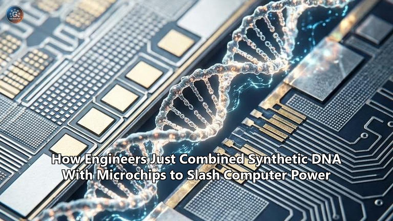
Inside a cleanroom at Pennsylvania State University’s Materials Research Institute, an oscilloscope trace flickered with a reading that initially looked like calibration error. An experimental solid-state memory cell had just switched its state and held it under an applied potential of barely 0.08 volts.
Standard silicon flash memory typically requires between 10 and 20 volts to tunnel electrons through floating gates. Modern low-power dynamic random-access memory (DRAM) operates around 1.1 volts. Yet this microscopic test structure—a sandwich of crystalline perovskite semiconductor fused to engineered strands of synthetic genetic material—was operating at less than a tenth of that voltage, dissipating a power density of just 0.01 watts per square centimeter.
+-----------------------------------------------------------------------------+
|                     OPERATING VOLTAGE COMPARISON                            |
|                                                                             |
|  Legacy 3D NAND Flash       [ 12.0 V – 20.0 V ]                             |
|  DDR5 Silicon DRAM          [ 1.1 V ]                                       |
|  Low-Power SRAM Cache       [ 0.7 V – 0.9 V ]                               |
|  Bio-Hybrid DNA Memristor   [ < 0.1 V ]  <-- (Penn State Benchmark)        |
+-----------------------------------------------------------------------------+
The device had sustained its state without continuous electrical power, survived thermal stresses up to 393 Kelvin (120 degrees Celsius), and maintained a stable ON/OFF resistance ratio exceeding $10^5$ over weeks of ambient testing.
Engineers had long treated biology and microelectronics as fundamentally irreconcilable domains. Silicon fabrication requires high vacuum, toxic plasma etchants, and furnace temperatures exceeding 1,000 degrees Celsius. Biological polymers like DNA, by contrast, evolved in warm, saline water and dissolve or unravel under harsh physical stressors.
Recent laboratory breakthroughs have bridged that physical divide. By chemically re-engineering short synthetic DNA sequences and depositing them directly onto semiconductor substrates, researchers have created bio-hybrid memristors and microfluidic processing arrays that slash computer power demands by up to 99%.
This hybrid hardware addresses the fundamental structural bottleneck threatening modern computing: the physical energy cost of moving numbers between memory and processors in high-density artificial intelligence clusters.
The Forensic Trail: The Thermodynamic Collapse of Silicon
To understand why microchip designers turned to genetic macromolecules, one must look at the thermodynamic crisis taking place inside the world's leading data centers.
Over the past four decades, computing performance followed two predictable trajectories: Moore’s Law (the doubling of transistors per unit area) and Dennard scaling (the principle that as transistors shrink, their power density remains constant). Dennard scaling broke down around 2005 when sub-micron silicon gates became so thin that quantum tunneling caused current to leak continuously, generating unsustainable heat.
Moore’s Law is now encountering its own physical wall. As commercial foundries manufacture chips at sub-3-nanometer nodes, lithography tools must manipulate matter at atomic dimensions. At these scales, the resistance of copper interconnects skyrockets, and parasitic capacitance turns chip wiring into an array of energy-sapping micro-resistors.
+-----------------------------------------------------------------------------+
|                      THE VON NEUMANN BOTTLENECK                             |
|                                                                             |
|   +-------------------+                     +------------------+            |
|   |   CPU / GPU Core  |  <=== High Energy = |   DRAM Memory    |            |
|   |                   |  === Data Shuttle = |                  |            |
|   | (0.1 - 2 pJ / op) |       (20 - 50 pJ)  |  (Capacitor leak)|            |
|   +-------------------+                     +------------------+            |
|                                                                             |
|   * Up to 80% of energy in AI workloads is lost during physical data bus    |
|     transport between separate logic and storage silicon.                   |
+-----------------------------------------------------------------------------+
The deeper issue is architectural: the von Neumann bottleneck. In conventional computers, logic processing (the central processing unit or graphics processor) and memory storage (DRAM or NAND flash) reside in physically segregated locations on the motherboard or silicon substrate.
Every time an artificial intelligence model calculates a weight update or an inference vector, data must travel across metal conductors from memory to logic, undergo calculation, and return to memory.
Physical measurements reveal the cost of this separation:
- Executing a floating-point multiplication on a modern arithmetic logic unit consumes approximately 0.1 to 2 picojoules ($10^{-12}\text{ J}$) of energy.
- Pulling the two numbers required for that calculation across a memory bus from off-chip DRAM consumes between 20 and 50 picojoules—up to 500 times more energy than the computation itself.
- In large language models with hundreds of billions of parameters, between 60% and 80% of the total electrical power is dissipated as waste heat simply moving charge back and forth across physical wires.
The International Energy Agency projects that electrical consumption from data centers, driven primarily by generative AI workloads, will exceed 1,000 terawatt-hours annually before 2030—roughly matching the total electricity consumption of Japan.
Silicon cannot solve this problem simply by scaling smaller. Shuffling electrons across inorganic wires to retrieve static bits has hit a hard thermodynamic limit.
Deconstructing the "Spaghetti Problem"
For decades, theoretical physicists pointed to nature’s data storage architecture as the obvious alternative. Deoxyribonucleic acid (DNA) stores the entire blueprint of a living organism within microscopic cell nuclei. In terms of sheer information density, a single gram of DNA can theoretically store roughly 215 petabytes (215 million gigabytes) of data. That is enough density to pack the contents of a warehouse-scale data center into a volume smaller than a sugar cube.
Furthermore, DNA retains its structural stability at room temperature for thousands of years without requiring an electric current. Silicon DRAM, by contrast, relies on microscopic capacitors that leak charge every few milliseconds, requiring constant "refresh" cycles that burn baseline electrical power even when the computer sits idle.
+-----------------------------------------------------------------------------+
|                      STORAGE MEDIUM DENSITY & LIFESPAN                      |
|                                                                             |
|  Medium                  Storage Density               Data Retention       |
|  -------------------------------------------------------------------------  |
|  Magnetic Tape           ~10^9 bytes/mm³               10 - 30 years        |
|  Silicon 3D NAND Flash   ~10^11 bytes/mm³              5 - 10 years         |
|  DNA Molecular Lattice   ~10^18 bytes/mm³              1,000 - 10,000+ yrs  |
+-----------------------------------------------------------------------------+
Yet past attempts to use biological DNA inside computer hardware hit a barrier. Biological DNA extracted from organisms consists of long, floppy polymers made of hundreds of thousands of base pairs. When placed on a solid-state chip, these macro-strands tangle into disordered molecular mats.
"Natural DNA behaves like wet spaghetti when you handle it at the nanoscale," explains Dr. Neela H. Yennawar, research professor and director of the Biomolecular Interactions Core Facility at the Huck Institutes of the Life Sciences. "It knots, it loops unpredictably, and its electrical conductivity is erratic. You cannot build a dependable, nanoscale logic circuit or memory gate when your conductive pathways change shape every time the humidity or temperature shifts".
Raw DNA is also a poor electrical conductor. Its sugar-phosphate backbone acts as an insulator, and charge transport across natural base pairs typically decays exponentially over distances greater than a few nanometers. To build functional computational hardware, engineers had to abandon natural biological DNA entirely.
The solution came from synthetic biology: designing short, custom-sequenced DNA oligomers from scratch.
Instead of isolating genetic material from cells, researchers engineered rigid, single-stranded oligonucleotides exactly 22 base pairs long. These synthetic strands act like structural girders rather than biological templates. They are predictable in length, rigid enough to align vertically on a substrate, and capable of being chemically tailored with atom-scale precision.
The Synthesis Breakthrough: Writing DNA Directly on Silicon
Before synthetic DNA could be combined with microchips to reduce power consumption, engineers faced an upstream chemical obstacle: traditional methods for making synthetic DNA were too slow, energy-intensive, and dirty to integrate into semiconductor packaging.
For decades, synthetic DNA was produced via phosphoramidite chemistry. This process relies on hazardous organic solvents like acetonitrile and dichloromethane, generating substantial toxic chemical waste while requiring large, climate-controlled synthesis instruments. Phosphoramidite synthesis occurs in batches and cannot be executed directly on the surface of active, delicate microelectronics without corroding the metal pads and passivation layers of the chip.
+-----------------------------------------------------------------------------+
|                     CMOS-INTEGRATED ENZYMATIC SYNTHESIS                     |
|                                                                             |
|      Electrode Ring A (+)              Reaction Site             Electrode Ring B (-)
|   [ Generates Local Protons ]     [ DNA Oligomer Growth ]     [ Neutralizes Acid Drift ]
|         (pH drops to ~4.5)            (TdT Polymerase)             (Protects Array)
|   ========================================================================= |
|                      CMOS SILICON CONTROL LAYER                             |
+-----------------------------------------------------------------------------+
A research team at Harvard University’s John A. Paulson School of Engineering and Applied Sciences, led by Professor Donhee Ham, bypassed this limitation by building a complementary metal-oxide-semiconductor (CMOS) silicon microchip that writes custom DNA sequences in water using electrical current.
Detailed in Nature Electronics, Ham’s team created a silicon array featuring 64 independent, micro-scale synthesis sites. Each site contains a central reaction zone surrounded by two concentric ring electrodes:
- The Inner Ring Electrode: When switched on by the underlying CMOS logic, the inner electrode drives a minute electrical current into the water, generating local protons via water electrolysis. This localized acidity drops the pH to an exact setpoint required for enzymatic deprotection.
- The Outer Ring Electrode: Simultaneously, the outer concentric ring consumes diffusing protons, preventing acidity from leaking to adjacent pixels on the chip.
- The Enzymatic Engine: An engineered enzyme—terminal deoxynucleotidyl transferase (TdT)—adds a single nucleotide (A, T, C, or G) to the growing DNA chain anchored to the silicon surface only where the electrical current is active.
By choreographing voltage pulses across the microchip array, the Harvard platform synthesizes 64 distinct DNA strands in parallel without using toxic solvents.
This method bridges the gap between digital semiconductor design and wet biological chemistry. It turns the silicon chip itself into the fabrication bed, setting the stage for direct integration of molecular polymers and solid-state circuitry.
Anatomy of a Bio-Hybrid Memristor
With precision synthetic oligonucleotides in hand, a multi-institution team led by researchers at Penn State University and the University of Cincinnati developed a hardware device that directly integrates these strands into solid-state microelectronic circuits.
Spearheaded by materials scientist Dr. Kavya S. Keremane and Professor Bed Poudel, the group sought to design a memristor—a memory resistor that natively retains its internal resistance state when powered off.
Memristors have long been viewed as the ideal component for compute-in-memory systems. Unlike binary transistors that switch between fully open (1) and fully closed (0), a memristor can alter its conductance across a continuous, analog spectrum.
This property mimics biological synapses in the human brain, which modulate the strength of connections between neurons.
+-----------------------------------------------------------------------------+
|                    BIO-HYBRID MEMRISTOR STACK ARCHITECTURE                  |
|                                                                             |
|   [ Top Electrode: Silver (Ag) ]                                            |
|   -----------------------------------------------------------------------   |
|   [ Semiconductor Layer: Quasi-2D Perovskite (PEA)₂(MA)Pb₂I₇ ]             |
|   -----------------------------------------------------------------------   |
|   [ Bio-Molecular Interface: Silver-Doped 22-mer Synthetic DNA (Ag-synDNA) ]|
|   -----------------------------------------------------------------------   |
|   [ Bottom Electrode: Platinum (Pt) Substrate ]                             |
+-----------------------------------------------------------------------------+
The device architecture relies on a specialized four-tier thin-film stack:
- The Platinum (Pt) Base: A bottom electrode substrate providing a stable, non-reactive electrical backplane.
- The Silver-Doped Synthetic DNA Layer (Ag-synDNA): A monolayer of custom 22-mer synthetic DNA sequences chemically synthesized and decorated with silver nanoparticles.
- The Quasi-2D Halide Perovskite Film ((PEA)₂(MA)Pb₂I₇): A crystalline organic-inorganic semiconductor layer combining phenylethylammonium (PEA) and methylammonium (MA) lead iodide.
- The Silver (Ag) Top Contact: An active metal electrode that serves as an ion reservoir during switching events.
"Biology and electronics operate on different physical principles," says Dr. Keremane. "Bridging these two worlds required creating an entirely new materials platform. If you place raw biomolecules on standard silicon, you get massive interfacial trap states, charge recombination, and immediate device breakdown. By combining engineered synthetic DNA with quasi-2D perovskites, we discovered a molecular synergy that stabilizes the entire electrical interface".
The Nanoscale Switching Mechanism
The device functions via electric field-driven ion migration and molecular orbital alignment.
When a positive voltage is applied to the top silver electrode, silver atoms oxidize into mobile cations ($\text{Ag}^+$). Driven by the electric field, these ions drift through the quasi-two-dimensional layers of the perovskite lattice.
+-----------------------------------------------------------------------------+
|                     CONDUCTION FILAMENT FORMATION                           |
|                                                                             |
|      [ Ag Top Electrode ]                      [ Ag Top Electrode ]         |
|              |                                          |                   |
|              v (E-field applied)                        | (Conductive path) |
|         Ag+  Ag+  Ag+                                  [Ag]                 |
|              |                                          |                   |
|              v                                         [Ag]                 |
|       (DNA π-π Channel)                                 |                   |
|              |                                         [Ag]                 |
|              v                                          |                   |
|      [ Pt Bottom Contact ]                     [ Pt Bottom Contact ]        |
|                                                                             |
|     HIGH RESISTANCE STATE (OFF)                 LOW RESISTANCE STATE (ON)   |
|      Voltage < 0.08 V                            Filament Bridged Across    |
+-----------------------------------------------------------------------------+
In conventional inorganic memristors, these metal ions wander haphazardly through grain boundaries, requiring high voltages (typically 1.5 to 5 volts) to force the formation of a continuous conductive filament. This random percolation creates unstable switching, generates excess heat, and degrades device endurance.
The synthetic DNA layer acts as a molecular guide. The 22-base-pair synthetic oligonucleotides are doped with silver ions that sit within the major and minor grooves of the double helix.
Computational modeling and structural analysis using PyMOL revealed that the organic cations of the perovskite undergo spontaneous $\pi\text{–}\pi$ stacking interactions with the aromatic ring bases (adenine, thymine, guanine, and cytosine) of the synthetic DNA.
This molecular ordering creates low-energy pathways. When the electric field is switched on, $\text{Ag}^+$ ions follow the pre-aligned DNA channels.
Instead of forcing a conductive bridge through bulk material, the ions slide down the DNA-perovskite interface, forming a stable metallic filament at an operational threshold under 0.1 volts.
Reversing the electrical polarity dissolves the silver filament back into the reservoir, returning the memristor to its high-resistance state. The entire cycle requires an operating power density of roughly 0.01 W/cm²—hundreds of times lower than conventional memory devices.
Lab Data: Performance Verification
The research team subjected the bio-hybrid memristors to standardized electrical and environmental tests to verify device stability:
+-----------------------------------------------------------------------------+
|                    EXPERIMENTAL BENCHMARK RESULTS                           |
|                                                                             |
|  Metric                     Measured Value          Silicon / Oxide Baseline|
|  -------------------------------------------------------------------------  |
|  Operating Threshold        0.08 V – 0.10 V         1.2 V – 3.3 V           |
|  Power Consumption Ratio    1/10th to 1/100th       1.0x (Standard Ref)     |
|  ON/OFF Current Ratio       > 10^5                  10^2 – 10^3             |
|  Thermal Survival Limit     393 K (120 °C / 248 °F) 358 K (85 °C standard)  |
|  Continuous Ambient Test    > 6 Weeks (Stable)      Degrades without seal   |
|  Cyclic Endurance           > 10^3 switching runs   10^2 – 10^3 for organics|
+-----------------------------------------------------------------------------+
The bio-hybrid device achieved an ON/OFF resistance ratio exceeding $10^5$. This wide operational window allows reading states with low current draw without signal errors caused by thermal noise.
The memristor also demonstrated multi-level data storage. By modulating the input compliance current between 1 microampere ($\mu\text{A}$) and 100 milliamperes ($\text{mA}$), the researchers configured the device to rest at intermediate analog resistance states.
This step confirms that the platform can process analog values directly in memory rather than just storing digital binary bits.
The Shift to In-Memory Computing
The convergence of biological polymers and semiconductor materials provides a physical foundation for synthetic DNA computing.
In a standard digital computer, running an artificial neural network requires breaking down mathematical operations into binary logic gates (AND, OR, NOT).
A matrix multiplication—the fundamental mathematical kernel of machine learning—requires fetching thousands of weights from memory, loading them into cache registers, calculating products using millions of transistors, and storing the output back into memory.
+-----------------------------------------------------------------------------+
|                     CROSSBAR IN-MEMORY VECTOR MULTIPLY                      |
|                                                                             |
|   Input Voltages                                                            |
|      (V1) -----[ G11 ]-----[ G12 ]-----[ G13 ]-----> Column 1 Current (I1)  |
|                   |           |           |          I1 = V1*G11 + V2*G21   |
|      (V2) -----[ G21 ]-----[ G22 ]-----[ G23 ]-----> Column 2 Current (I2)  |
|                   |           |           |          I2 = V1*G12 + V2*G22   |
|                                                                             |
|   * Calculation occurs INSTANTANEOUSLY via Ohm's Law (I = V * G)            |
|     and Kirchhoff's Current Law (Itotal = Sum of I).                        |
|   * ZERO dynamic shuttling of matrix weights across an off-chip bus.        |
+-----------------------------------------------------------------------------+
Bio-hybrid memristors execute matrix multiplication differently:
- Ohm’s Law ($I = V \times G$): When an input voltage ($V$) representing an incoming signal is fed into a DNA-perovskite memristor, the current ($I$) flowing through the device is proportional to its internal conductance ($G$). The physical device executes multiplication analogously in real time.
- Kirchhoff’s Current Law ($I_{\text{total}} = \sum I_k$): When multiple memristors are arranged in a crossbar array, the currents flowing down each column automatically sum together at the output wire.
The matrix multiplication happens within the physical material itself, eliminating the need to transport data over a system bus.
Because the DNA-perovskite channels switch at sub-0.1-volt levels, an entire matrix calculation consumes fractions of the energy required by a silicon GPU.
The computational workload shifts from shuffling billions of digital electrons across parasitic wires to reading small, localized current flows guided by organized molecular strands.
Molecular Logic and Strand Displacement
Beyond solid-state memristor architectures, another branch of synthetic DNA computing operates entirely through chemical interactions. This approach, known as DNA strand displacement (DSD), uses the thermodynamics of base pairing to perform computation without electrical currents.
In a strand displacement circuit, pre-hybridized double strands of synthetic DNA act as logic gates. When a single-stranded "input" DNA molecule with a specific base sequence is introduced, it binds to an exposed single-stranded overhang (a toehold) on the gate molecule.
+-----------------------------------------------------------------------------+
|                      DNA STRAND DISPLACEMENT (DSD)                          |
|                                                                             |
|  Input Strand:      [ Toehold A' ][   Recognition Domain B'   ]             |
|                            |                                                |
|                            v (Binds to exposed Toehold A)                   |
|  Target Gate:       [ Toehold A  ][ Domain B ][ Displaced Output C ]        |
|                                                                             |
|  Reaction Outcome:                                                          |
|  [ Bound Complex: A-A' / B-B' ]   +   [ Released Output Strand: C ]         |
|                                                                             |
|  * Released Output C cascades forward to trigger downstream DNA gates.       |
|  * Operates at room temperature; consumes zeptojoules (10^-21 J) per step.  |
+-----------------------------------------------------------------------------+
Because the base-pairing affinity between the input strand and the template is thermodynamically stronger than the gate’s existing bond, the input strand unzips the original partner strand and releases it into solution.
This released output strand then acts as an input for the next molecular gate, creating cascading logic operations.
- Zero Dynamic Power Consumption: Once synthetic strands are mixed in an aqueous medium or stabilized within a microfluidic channel, strand displacement reactions run autonomously driven entirely by the free energy ($\Delta G$) of hybridization. They require no electrical power supply or clock generator.
- Massive Parallelism: A small microfluidic chamber can contain more than $10^{15}$ individual DNA strands reacting simultaneously. A silicon processor executes instructions sequentially or across hundreds of GPU cores; a molecular solution computes trillions of displacement reactions concurrently across its volume.
- Energy per Operation: Whereas a standard silicon transistor burns roughly $10^{-15}$ joules (femtojoules) per switching event, a DNA strand displacement reaction operates near the thermodynamic limit: approximately $10^{-21}$ joules (zeptojoules) per step.
Microchips are now used to control these molecular reactions directly. Microfluidic processing units (MPUs) integrated with microelectronic control layers use digitally actuated microscopic valves, micro-heaters, and photodetectors to route, heat, and read out DNA computation steps on a single board.
+-----------------------------------------------------------------------------+
|                   HYBRID MICROFLUIDIC-CMOS PROCESSING STACK                 |
|                                                                             |
|   +---------------------------------------------------------------------+   |
|   | Microfluidic Routing Layer: Channels, Valves, DNA Reagent Chambers  |   |
|   +---------------------------------------------------------------------+   |
|   | Sensing & Heating Layer: Micro-heaters, OLED Emitters, Photodiodes  |   |
|   +---------------------------------------------------------------------+   |
|   | Control Logic Layer: Standard CMOS Silicon Processing Core          |   |
|   +---------------------------------------------------------------------+   |
+-----------------------------------------------------------------------------+
Institutes like Fraunhofer IPMS, through its BIOSYNTH platform, have integrated microfluidic channels directly onto CMOS silicon wafers.
These hybrid chips use tiny integrated micro-heaters to trigger thermal DNA synthesis and molecular logic reactions, while embedded organic light-emitting diodes (OLEDs) and integrated photodiodes monitor hybridization results in real time.
This architecture provides the control of digital microprocessors alongside the energy-efficient parallelism of molecular chemistry.
Overcoming the Stability and Temperature Obstacles
When bio-hybrid computing was first proposed, semiconductor engineers raised practical objections:
- How can organic biological materials survive inside electronics running at elevated temperatures?
- Wouldn't ambient humidity destroy the molecular structures within days?
- Would DNA-perovskite devices degrade under continuous electrical switching?
Addressing these questions was central to the Penn State and University of Cincinnati study.
Biological DNA in liquid solution denatures (its double strands pull apart into single strands) between 60 and 90 degrees Celsius. However, when short synthetic DNA strands are vacuum-deposited and intercalated with silver ions, their structural dynamics change.
+-----------------------------------------------------------------------------+
|                      MOLECULAR CONFINEMENT & STABILIZATION                  |
|                                                                             |
|              [ Quasi-2D Inorganic Halide Perovskite Layer ]                 |
|                                |   |   |                                    |
|                      π-π Stacking Intercalation                             |
|                                |   |   |                                    |
|              [ Silver-Ion Crosslinked Synthetic Oligomers ]                 |
|                                                                             |
|   * Intermolecular π-π stacking immobilizes base pairs against heat.         |
|   * Dense ionic coordination with silver ions prevents thermal unraveling.   |
|   * Perovskite layers act as an oxygen and moisture barrier.                |
+-----------------------------------------------------------------------------+
The device survived continuous operation at 393 Kelvin (120 degrees Celsius / 248 degrees Fahrenheit)—well above the operating temperature limits of commercial silicon CPUs and GPUs.
Three structural mechanisms explain this durability:
- Geometric Confinement: Trapped within the layered lattice of the quasi-2D perovskite, the 22-mer synthetic DNA strands lack the physical space needed to unwind or denature.
- Ionic Coordination: Silver nanoparticles form coordination bonds with the nitrogenous ring bases of the DNA, cross-linking the molecular strands into a robust, semi-rigid organometallic framework.
- $\pi\text{–}\pi$ Stacking Anchors: The thermodynamic interactions between the aromatic groups of the perovskite cations and the DNA nucleobases distribute mechanical and thermal stress across the interface.
During long-term endurance trials, test devices operated in ambient open air for six consecutive weeks without showing significant degradation in switching margins or current retention.
Cleanroom and Manufacturing Roadblocks
Despite these laboratory successes, integrating biological macromolecules into industrial semiconductor manufacturing faces practical industry challenges.
Commercial fabrication facilities (fabs) operated by TSMC, Intel, and Samsung are among the most strictly controlled manufacturing environments in the world. Modern cleanrooms exclude foreign elements to prevent contaminating silicon wafers.
Historically, copper was banned from leading-edge fabs for years due to concerns that it would diffuse into silicon substrates and ruin transistors.
+-----------------------------------------------------------------------------+
|                     FAB INTEGRATION CHALLENGES & SOLUTIONS                  |
|                                                                             |
|  Contamination Risk:                                                        |
|  * Biomolecules & silver ions cannot enter ultra-pure Front-End cleanrooms. |
|                                                                             |
|  Manufacturing Solutions:                                                   |
|  1. Back-End-of-Line (BEOL) Integration: Deposit bio-hybrid materials only   |
|     during final metal layer steps, isolating sensitive silicon transistors.|
|  2. Chiplet Co-Packaging: Fabricate standard CMOS logic and bio-hybrid       |
|     memristor dies on separate lines, joining them via silicon interposers. |
+-----------------------------------------------------------------------------+
Synthetic DNA and quasi-2D lead halide perovskites introduce materials that silicon foundries treat with caution:
- Organic Contamination: High-temperature semiconductor tools cannot be exposed to carbon-rich organic compounds, which outgas and contaminate vacuum chambers.
- Heavy Metal and Halide Migration: Halide perovskites contain lead and iodine ions that diffuse rapidly through silicon dioxide dielectric layers if not sealed by barrier liners.
Because of these constraints, the commercial deployment of synthetic DNA computing will not occur via monolithic integration inside front-end silicon fabs.
Instead, two packaging pathways are emerging across the semiconductor supply chain:
1. Back-End-of-Line (BEOL) Post-Processing
In this integration model, the base CMOS silicon wafer—containing standard logic transistors, clock trees, and input/output circuits—is fabricated using standard high-temperature semiconductor lines.
The wafer is then transferred to a secondary, low-temperature back-end facility where metal interconnect lines, barrier nitrides, and passivation stacks are applied.
The synthetic DNA and perovskite layers are deposited at temperatures below 150 degrees Celsius directly onto the top-level copper or platinum metal pads, keeping the cleanroom processing lines separated.
2. Heterogeneous 2.5D/3D Chiplet Packaging
Rather than placing biomaterials directly onto the silicon wafer, foundries can build modular chiplet modules:
- The control logic, analog-to-digital converters, and host CPU interfaces are manufactured on standard CMOS wafers.
- The bio-hybrid memristor crossbars or microfluidic DNA storage arrays are fabricated on dedicated glass or quartz substrates.
- Both dies are joined side by side on a high-density silicon interposer using micro-bumps or bonded in a 3D vertical stack using through-silicon vias (TSVs).
This modular approach isolates novel bio-hybrid materials within dedicated physical packages, allowing chipmakers to leverage existing manufacturing ecosystems without redesigning cleanroom infrastructure.
Synthesis Costs and Throughput Realities
While the energy efficiency of bio-hybrid memory devices during inference and read/write operations is clear, the economics of synthesizing custom DNA strands remain a cost bottleneck.
+-----------------------------------------------------------------------------+
|                      DNA SYNTHESIS COST TRAJECTORY                          |
|                                                                             |
|  Year       Cost Per Megabase (Oligos)      Synthesis Method                |
|  -------------------------------------------------------------------------  |
|  2010       ~$10,000                        Column Phosphoramidite          |
|  2018       ~$100                           High-Density Microarray         |
|  2026       ~$0.50 – $2.00                  Enzymatic / CMOS-Assisted       |
|  2030 (Proj) <$0.001                        Continuous On-Chip Enzymatic    |
+-----------------------------------------------------------------------------+
Although sequencing (reading) DNA has dropped in cost at a rate faster than Moore’s Law—falling from $100 million per human genome in 2001 to less than $200 today—synthesis (writing) remains more expensive.
For bio-hybrid memristors, this upfront cost is mitigated because the DNA is not discarded as a consumable reagent.
Instead, once a 22-mer sequence is synthesized and integrated into the thin-film layer of the chip, it serves as permanent physical hardware. The same fixed molecular array switches repeatedly across billions of operations without requiring new DNA synthesis.
The cost challenge applies primarily to DNA storage applications, where new data requires continuously synthesizing new sequence chains.
The transition from column-based phosphoramidite chemistry to CMOS-driven enzymatic synthesis in water, demonstrated by teams at Harvard, Fraunhofer, and startups like Molecular Assemblies and Iridia, will be critical to lowering synthesis costs to commercial viability.
The Broader Landscape: A Comparative Look
To understand how bio-hybrid synthetic DNA microchips fit into the computing ecosystem, engineers compare their operating parameters with alternative computing architectures:
+-----------------------------------------------------------------------------+
|                 EMERGING LOW-POWER COMPUTING ARCHITECTURES                  |
|                                                                             |
|  Architecture       Energy / Op       Data Density     Commercial Readiness |
|  -------------------------------------------------------------------------  |
|  Advanced CMOS GPU  ~10^-12 J (pJ)    Moderate         Now in Production    |
|  Silicon Neuromorphic                                                       |
|  (e.g., Loihi 2)    ~10^-14 J (tens fJ) Moderate       Pilot Production     |
|  Inorganic RRAM     ~10^-13 J (100 fJ) High            Early Commercial     |
|  Photonic Chips     ~10^-15 J (fJ)    Low              Specialized Scaling  |
|  Bio-Hybrid DNA                                                             |
|  Memristor          ~10^-16 J (sub-fJ) Ultra-High      Cleanroom Prototyping|
|  Aqueous DNA (DSD)  ~10^-21 J (zJ)    Extreme (3D)     Laboratory Arrays    |
+-----------------------------------------------------------------------------+
Silicon neuromorphic processors, such as Intel’s Loihi 2, achieve significant energy reductions by executing spiking neural networks that transmit current only when a neuron fires.
However, they remain constrained by standard silicon transistor physics, operating at standard voltages between 0.7 and 0.9 volts.
Photonic microchips use light through silicon waveguides to execute matrix multiplication with low latency, but their components occupy significant physical area—often millimeters per optical node—making high-density memory arrays difficult to scale.
Bio-hybrid synthetic DNA chips bridge these performance metrics:
- They provide the sub-0.1-volt operating levels and high thermal endurance of engineered organometallic films.
- They deliver high physical storage density and synaptic analog functionality.
- They can be fabricated via low-temperature back-end methods compatible with existing silicon packaging technologies.
What to Watch Next
The successful demonstration of stable, low-voltage bio-hybrid memristors in the laboratory marks an important engineering milestone, transitioning synthetic biology from life-science applications into functional computational hardware.
The timeline for scaling this platform to commercial utility depends on several technical milestones:
+-----------------------------------------------------------------------------+
|                      DEVELOPMENT ROADMAP & MILESTONES                       |
|                                                                             |
|  Phase 1: 1-Kilobit Crossbar Arrays (2026 - 2027)                          |
|  * Demonstrate multi-bit matrix multiply on fully integrated 32x32 arrays.  |
|  * Benchmark error correction code (ECC) requirements for bio-interfaces.   |
|                                                                             |
|  Phase 2: Hybrid CMOS-Bio Co-Packaging (2027 - 2028)                        |
|  * Tape-out first 2.5D chiplet pairing RISC-V controller with DNA memory.   |
|  * Establish baseline foundry yield benchmarks for back-end DNA deposition. |
|                                                                             |
|  Phase 3: Edge AI & Ultra-Low-Power Commercial Deployments (2029 - 2030+)   |
|  * Deploy non-volatile bio-memristors in battery-free IoT & space systems.  |
|  * Scale high-speed enzymatic on-chip synthesis for mass data archives.     |
+-----------------------------------------------------------------------------+
Key milestones and questions to track include:
- Kilobit-Scale Crossbar Scaling: Research groups must scale from single laboratory test cells to dense $32 \times 32$ and $64 \times 64$ crossbar arrays. This step will verify whether sneak-path leakage currents can be managed across thousands of adjacent bio-hybrid junctions without degrading signal readouts.
- Cycling Endurance Beyond $10^6$ Cycles: The initial tests demonstrated stable endurance through $10^3$ cycles. While this is sufficient for non-volatile storage and edge AI inference weights, neuromorphic chips running continuous on-chip training will require endurance limits exceeding millions of cycles.
- Standardizing Bio-Packaging Materials: Establishing standardized passivation and encapsulation coatings (such as atomic-layer-deposited aluminum oxides and Parylene barriers) will be critical to isolate perovskite-DNA interfaces from environmental degradation.
- Direct Integration with Open-Source Architectures: Watch for academic and industrial partnerships integrating bio-hybrid analog crossbars with open-source RISC-V microcontrollers, creating hybrid digital-molecular processors for energy-constrained edge devices.
As high-density artificial intelligence models place growing demands on regional power grids and silicon fabs push the physical limits of sub-nanometer lithography, microchip designers are expanding beyond traditional materials.
By combining the structural programming of synthetic DNA with the electronic properties of advanced semiconductors, engineers are showing that the biological polymers that store life's genetic instructions can also help power the future of computing.
Reference:
- https://www.google.com/search?q=time+in+Centre+County,+US
- https://www.psu.edu/news/research/story/borrowing-biology-power-next-gen-data-storage
- https://www.perovskite-info.com/new-dna-perovskite-memristors-achieve-100x-lower-power-neuromorphic-computing
- https://www.techradar.com/pro/nature-has-the-solution-researchers-fuse-dna-and-silicon-to-build-holy-grail-of-memory-storage
- https://bioengineer.org/harnessing-biology-to-drive-next-generation-data-storage/
- https://www.sciencedaily.com/releases/2026/08/260816044853.htm
- https://www.futura-sciences.com/en/after-decades-of-calculations-microchips-now-start-creating-synthetic-dna-heres-how_36538/
- https://scitechdaily.com/dna-meets-electronics-scientists-create-ultra-low-power-memory-breakthrough/
- https://www.sciencedaily.com/releases/2026/08/260816044853.htm
- https://www.facebook.com/Digitalleaderspakistan/posts/nature-has-been-storing-data-in-dna-for-billions-of-years-penn-state-just-figure/1231195265892921/
- https://www.facebook.com/thebrainmazeofficial/videos/scientists-store-data-in-dna-what-if-the-key-to-storing-humanitys-endless-data-w/1849461545993537/
- https://seas.harvard.edu/news/making-dna-semiconductor-chip
- https://www.sciencedaily.com/releases/2026/07/260708022202.htm
- https://semiengineering.com/research-bits-apr-14/
- https://www.researchgate.net/publication/10952821_Computing_with_DNA_Although_DNA_clearly_outclasses_any_silicon-based_computer_when_it_comes_to_information_storage_and_processing_speed_a_DNA-based_PC_is_still_a_long_way_off
- https://embeddedcomputing.com/technology/storage/how-synthetic-dna-for-data-storage-could-help-the-memory-crisis
- https://www.mackenziemorehead.com/i-i-addendum-dna-based-data-storage/
- https://www.fraunhofer.de/en/press/research-news/2025/may-2025/synthetic-dna-as-mass-data-storage-of-the-future.html
- https://syntecoptics.com/dna-computing-microfluidic-chips/
- https://unescoalfozanprize.org/silicon-chip-uses-electricity-to-write-dna-in-major-biotech-breakthrough/
- https://dnastoragealliance.org/publications/
- https://www.matse.psu.edu/directory/kavyashree-keremane