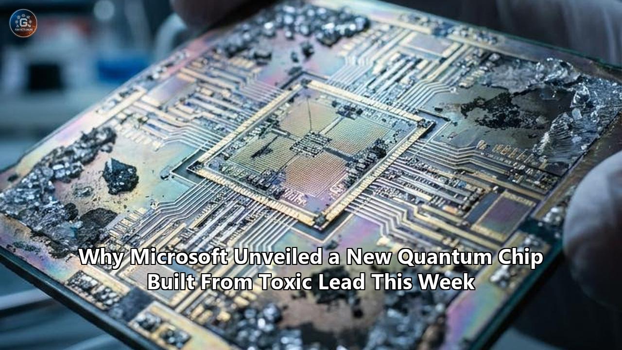
On June 2, 2026, at its annual Build developer conference in San Francisco, Microsoft shook the quantum computing landscape by unveiling a new physical architecture that deliberately embraces one of the most notoriously difficult, toxic, and delicate metals on the periodic table: lead.
The announcement of the Majorana 2 processor marks a dramatic pivot in Microsoft’s long-term, multi-billion-dollar bet on topological quantum computing. For more than a decade, the tech giant has stood virtually alone in its refusal to build standard, noisy superconducting qubits. Instead, it has chased the elusive Majorana fermion—a subatomic quasiparticle that is its own antiparticle, capable of "braiding" information across space and time to create qubits that are theoretically immune to environmental noise.
With the debut of Majorana 2, Microsoft claims it has achieved a monumental materials science breakthrough by replacing traditional aluminum superconductors with lead. The result is a Microsoft quantum chip that boasts a 1,000-fold improvement in qubit reliability over its predecessor, stretching average qubit "parity" lifetimes from milliseconds to an average of 20 seconds, with some lasting up to a full minute.
+-------------------------------------------------------------------------+
|                    QUBIT PARITY LIFETIME COMPARISON                    |
+-------------------------------------------------------------------------+
| Majorana 1 (Aluminum)  |   1 to 12 Milliseconds                  |
+--------------------------------+----------------------------------------+
| Majorana 2 (Lead)      |   20 to 60 Seconds (1,000x Increase)   |
+--------------------------------+----------------------------------------+
| Superconducting Qubits |   Microseconds (Highly unstable)       |
+-------------------------------------------------------------------------+
This sudden jump in stability has prompted Microsoft to halve its commercial timeline. The company now asserts it will deliver a fully scalable, commercially viable quantum computer by 2029.
However, the decision to construct a Microsoft quantum chip from lead has introduced a bizarre and dangerous manufacturing crisis. Lead is not only highly toxic to handle at scale, but it is also water-soluble during specialized semiconductor wet-etching procedures, meaning it literally dissolves and washes away during standard microfabrication.
To overcome this, Microsoft had to rely on a suite of autonomous, agentic AI tools known as "Microsoft Discovery" to engineer an entirely water-free fabrication process. This software-hardware co-design highlights the intense, high-stakes competition between Microsoft and rivals like IBM, Google, and Quantinuum, each of whom is pursuing radically different physical approaches to the same holy grail of computing.
The Metallic Gamble: Why Microsoft Swapped Aluminum for Lead
To understand why Microsoft went to such extreme lengths to put toxic lead on a quantum processor, one must first look at the physics of the "topological gap".
In a topological quantum computer, qubits are not made from isolated, fragile physical particles that can be easily disturbed by a stray thermal vibration or a cosmic ray. Instead, Microsoft constructs nanowires out of a semiconductor-superconductor hybrid material. When these nanowires are cooled to near absolute zero (approximately 10 millikelvins, colder than deep space) and subjected to a precise magnetic field, they enter a topological phase.
At the ends of these nanowires, Majorana zero modes emerge. Because the quantum information is stored non-locally—split between the two ends of the wire—a local disturbance at one end cannot corrupt the data. This is hardware-level protection.
However, the strength of this protection is dictated entirely by the "topological gap," which acts as an energy barrier. If the gap is too small, even tiny amounts of residual thermal energy or environmental noise can jump the barrier, destroying the topological phase and causing the qubit to decohere.
In its first-generation Majorana chip (unveiled in early 2025), Microsoft utilized aluminum as the superconducting layer. Aluminum is the absolute darling of the semiconductor and quantum industries; it is cheap, easy to deposit, highly understood, and non-toxic. But aluminum has a fundamental physical limitation: its superconducting transition temperature is low, and its pairing energy gap is relatively weak. Consequently, the topological gap on the original Majorana chip was narrow, limiting qubit parity lifetimes to a fragile window between 1 and 12 milliseconds.
                 === THE TOPOLOGICAL GAP GAPING ===

   [Aluminum Superconductor]              [Lead Superconductor]
   =========================              =====================
      Thermal/Cosmic Noise                   Thermal/Cosmic Noise
             |                                      |
             v                                      x  (Blocked!)
      --------------                                -----
      Topological Gap                              Topological Gap
      (Narrow Energy Barrier)                      (Doubled Energy Barrier)
      --------------                                -----
             |
             v
      Qubit Decoheres                        Qubit Remains Stable
      (Lifetime: ~1-12 ms)                   (Lifetime: 20-60 seconds)
To widen this gap, Microsoft’s quantum team had to find a superconductor with a much higher critical temperature and stronger electron coupling. Lead (Pb) was the ideal candidate. Its larger atomic radius and robust superconducting properties allowed the team to more than double the topological gap of the device.
According to Chetan Nayak, Technical Fellow and Corporate Vice President of Quantum Hardware at Microsoft, this materials swap fundamentally changed the stability profile of the topological phase. The wider gap engineered by the lead-based material stack effectively shields the fragile qubits from external disturbances. This protective envelope is what allowed Microsoft’s Copenhagen and Redmond labs to push qubit parity lifetimes up to 20 seconds, with exceptional instances maintaining their state for more than a minute.
In a field where rivals measure qubit lifetimes in fractions of a millisecond, a 20-second lifetime is an eternity. It is the quantum equivalent of replacing a smartphone battery that dies in twenty minutes with one that lasts for several months on a single charge.
The Water-Soluble Nightmare: Fabricating with Toxic Lead
While the theoretical physics of lead-based superconductors have been known for decades, actually building a micro-scale silicon chip with lead has been a manufacturing impossibility.
"The reason why people don't use it to build chips is it requires an incredibly specialized process to be able to go figure that out," Jason Zander, Microsoft’s Executive Vice President overseeing quantum efforts, told Reuters. "And we figured it out."
The primary engineering obstacle is that lead is highly reactive and water-soluble during the standard, aggressive chemical processes used to etch micro-chips. In a typical cleanroom, semiconductor wafers are subjected to wet-etching baths, deionized water rinses, and liquid developer solutions. If you attempt to pattern ultra-thin lead nanowires using these traditional lithographic techniques, the lead literally dissolves and washes down the drain.
               TRADITIONAL VS. MICROSOFT WATER-FREE FABRICATION

   [Traditional Wet-Etching]              [Microsoft Water-Free Dry-Etching]
   =========================              ==================================
   1. Photoresist Patterning              1. Photoresist Patterning
   2. Wet-Chemical Bath (Water-based)     2. Specialized Dry-Gas Etching
   3. Lead Dissolves & Washes Away        3. Vacuum Deposition of Protective Cap
   RESULT: Ruined, broken wafer           RESULT: Intact, 10-nanometer Lead Wires
To circumvent this chemical roadblock, Microsoft’s engineering teams had to design an entirely closed-loop, water-free, dry-fabrication pipeline. The process requires depositing lead, antimony, indium arsenide, and indium arsenide antimonide in a highly controlled, ultra-high vacuum environment. Etching must be performed using specialized dry-gas plasma chemistries, and the resulting structure must be instantly capped with a protective passivating layer before it can ever be exposed to the ambient cleanroom atmosphere.
Managing this incredibly narrow, multi-variable fabrication window would have taken human scientists decades of trial-and-error. Microsoft accelerated this process using Microsoft Discovery, the company's agentic AI platform for scientific research and development, which officially hit general availability at Build 2026.
Rather than using AI merely to run simulations, Microsoft embedded teams of autonomous AI agents directly into the cleanroom workflow. Guided by human prompts, these AI agents analyzed real-time feedback from material deposition tools, searched academic literature for compatible non-aqueous solvents, automated microscopic measurements, and identified physical defects in the wafer substrates that were causing the lead structures to peel.
Zulfi Alam, Microsoft’s Corporate Vice President for Quantum Technologies, described the automation of these measurements and fabrication optimizations via agentic AI as the critical turning point of the entire program. Without the AI managing the microscopic adjustments needed to keep the lead from oxidizing or dissolving, the Majorana 2 processor would still be a theoretical concept on a blackboard.
The Topology Trade-Off: How Majorana Differs from the Rest
To appreciate why Microsoft is willing to battle the toxic, water-soluble headaches of lead fabrication, it is necessary to contrast their "topological" philosophy against the mainstream quantum computing industry.
Currently, the quantum race is divided into four primary physical architectures. Each approach features distinct advantages, but they all suffer from unique, brutal engineering trade-offs.
+---------------------------------------------------------------------------------------------------+
|                                 THE FOUR LEADING QUANTUM PATHS                                    |
+-------------------+----------------------------+-------------------------+------------------------+
| Architecture      | Key Developers             | Physical Qubit Size     | Primary Vulnerability  |
+-------------------+----------------------------+-------------------------+------------------------+
| Superconducting   | IBM, Google        | ~1.0 Millimeter         | Extreme noise; short   |
|                   |                            |                         | coherence                     | suspended ions)         | laser scaling bottleneck|
+-------------------+----------------------------+-------------------------+------------------------+
| Neutral Atom      | QuEra, Atom Computing [2.1.2| Atomic-scale (held by   | Optical complexity;    |
|                   | 2.1.4]                     | optical tweezers)       | loss of atoms  |
+-------------------+----------------------------+-------------------------+------------------------+
| Topological       | Microsoft          | ~0.01 Millimeter (Lead/ | Highly controversial;  |
|                   |                            | InAs stack).
*   **The Advantage:** Hardware-level error protection. Because the information is stored in the geometric arrangement (braiding) of the particles rather than the state of a single particle, local environmental noise cannot alter the state. This results in extremely small qubits (one-hundredth of a millimeter) and potentially a 1-to-1 or near 1-to-1 ratio of physical-to-logical qubits.
*   **The Drawback:** Unbelievably complex materials science. Since Majorana particles are quasiparticles (collective excitations of electrons), they must be carefully coaxed into existence using highly exotic, toxic material stacks that are exceptionally difficult to manufacture.

### 2. Superconducting Qubits (IBM, Google)
*   **The Concept:** Fabricate macroscopic LC circuits on silicon chips using aluminum wires. The quantum states are manipulated using microwave pulses.
*   **The Advantage:** Fast gate speeds (nanosecond scale) and high compatibility with existing semiconductor manufacturing plants.
*   **The Drawback:** Highly sensitive to noise. These qubits are physically large (~1 mm), making them easy targets for electromagnetic interference, thermal fluctuations, and cosmic rays. Because they are so noisy, superconducting architectures suffer from a massive "error-correction tax." To create just one error-corrected "logical" qubit, a system might require 1,000 or more noisy physical qubits, meaning a useful quantum computer will need millions of physical qubits to do real work.

### 3. Trapped-Ion Qubits (Quantinuum, IonQ)
*   **The Concept:** Suspend individual charged atoms (ions) in electromagnetic fields inside a vacuum chamber, manipulating their states using highly tuned lasers.
*   **The Advantage:** Because every atom of a given isotope is identical by nature, these qubits are perfectly uniform, eliminating manufacturing variability. They feature very long coherence times and some of the highest gate fidelities in the industry.
*   **The Drawback:** Extremely slow gate speeds compared to superconducting systems. Furthermore, physically scaling the architecture is a nightmare. It requires "shuttling" ions through complex electromagnetic traps (a process called the QCCD architecture) and focusing thousands of individual laser beams onto a tiny, vibrating array of atoms.

### 4. Neutral Atom Qubits (QuEra, Atom Computing)
*   **The Concept:** Use arrays of laser beams (optical tweezers) to trap and position neutral atoms in 2D or 3D grids, using Rydberg states to induce quantum entanglement.
*   **The Advantage:** Highly mobile qubits. You can physically move the atoms around mid-calculation to change the computer's wiring dynamically. They can package thousands of physical qubits into a space the size of a grain of sand without needing complex wire routing.
*   **The Drawback:** Complex optical control planes. Scaling to tens of thousands of qubits requires incredibly high-powered, precise laser systems. Additionally, if an atom accidentally escapes its optical tweezer, the system must pause to reload the trap, introducing latency.

Microsoft's bet is that the "error-correction tax" of superconducting systems is too high to ever be commercially viable. If a machine requires a million physical qubits to run 1,000 logical qubits, the physical footprint, cooling requirements, and control wiring of that machine will be the size of a football field, costing billions of dollars and consuming megawatts of power.

By building the **Microsoft quantum chip** out of lead, Microsoft is aiming to bypass this scaling wall entirely. If a topological qubit is inherently stable at the hardware level, they might only need a few physical qubits per logical qubit.

A system with just 10,000 tiny, 10-micrometer topological qubits could theoretically outperform a superconducting system with a million physical qubits, all while fitting inside a standard, commercial server rack.

---

## The Superconducting Giants: IBM’s $10 Billion Starling and Google’s Quiet Willow

Despite Microsoft’s progress with lead, the superconducting giants are not sitting idly by. They are pushing ahead with brute-force scaling, relying on massive capital and sophisticated error-correction software to overcome the inherent noisiness of their aluminum-based chips.

### IBM’s Centric-Supercomputer Strategy
Just as Microsoft announced Majorana 2, IBM reinforced its commanding lead in commercial quantum deployment. On June 2, 2026, IBM announced a staggering $10 billion investment over the next five years to accelerate its quantum roadmap.

IBM’s strategy has pivoted away from building single, massive, monolithic chips. Instead, they are pioneering "Quantum-Centric Supercomputing".

Using their 156-qubit Heron processor as a modular building block, IBM is linking multiple chips together within a single dilution refrigerator using ultra-fast, cryogenic microwave interconnects.
IBM'S MODULAR SUPERCONDUCTING APPROACH
+-----------------+ +-----------------+
| Heron QPU | | Heron QPU |
| (156 Qubits) | | (156 Qubits) |
+--------+--------+ +--------+--------+
| |
+-------->[ Cryo-Interconnect ]<--+
|
v
[ PCIe Gen 6 Real-time Control ]
|
v
+-------------------------------+
| NVIDIA GPU / CPU Supercluster |
+-------------------------------+
By integrating these QPUs side-by-side with NVIDIA-class GPU clusters over direct PCIe Gen 6 connections, IBM plans to deliver "Quantum Utility"—where quantum processors act as real-time computational accelerators for exascale workflows.

IBM is highly confident in this modular approach. They have stated that their partners will demonstrate the first concrete examples of practical "quantum advantage" by the end of 2026, using their Nighthawk processor running circuits with 7,500 gates across multiple 120-qubit modules.

By 2029—the same year Microsoft now targets for its first commercial machine—IBM plans to deploy "Starling," a fully fault-tolerant quantum computer with 200 logical qubits running 100 million gates.

### Google’s Below-Threshold Triumph
Google, meanwhile, is pursuing a strategy of "fewer but perfect" qubits. In May 2026, Google officially declared the end of the "noisy" quantum era with the introduction of its new "Willow" chip.

Running a complex out-of-order time correlator (OTOC) algorithm called "Quantum Echoes," the Willow chip performed a task in just 5 minutes that would take the world’s fastest classical supercomputers 10 septillion years to calculate.

But Google’s true triumph of 2026 lies in its empirical demonstration of below-threshold quantum error correction. In physical quantum systems, adding more qubits typically introduces more routes for noise to enter, increasing the overall error rate of the system.

In February 2026, Google proved that by scaling their superconducting grid from a 3x3 array up to a 7x7 array, the overall error rates of their logical qubits did not increase—they were cut in half at each step. One of their logical qubits actually lived twice as long as the best single physical qubit that comprised it.

Google’s roadmap remains fixed on building a 1-million-physical-qubit machine by 2029. Because they have proven that their error-correction code is operating below the critical physical threshold, Google’s leadership views the race to a million qubits not as an open-ended scientific mystery, but as a direct, well-defined engineering sprint.

---

## The Gas and Laser Alternatives: Trapped Ions and Neutral Atoms

While Microsoft battles materials toxicity and IBM and Google scale massive dilution refrigerators, a parallel front is unfolding in the public markets.

### Quantinuum’s Nasdaq Debut
Quantinuum, the trapped-ion giant carved out of Honeywell, is preparing to go public under the ticker QNT, targeting a valuation that could reach up to $14.2 billion.

Quantinuum’s competitive advantage lies in its sheer precision. Their current "Helios" system operates with a 99.921% average two-qubit gate fidelity—the highest verified accuracy rate in the entire quantum industry.

Because trapped ions are naturally identical and held in a pristine vacuum, they do not suffer from the microscopic structural defects that plague solid-state chips like Google’s aluminum circuits or Microsoft’s lead nanowires.

Quantinuum is already delivering 48 logical qubits on its Helios hardware, with plans to launch "Sol" (100 logical qubits) in 2027, and its fully commercial, fault-tolerant "Apollo" system in 2029.

However, Quantinuum faces severe commercial hurdles. The company lost $136.6 million in the first quarter of 2026 alone, reflecting the massive cash burn required to manufacture ultra-low-loss integrated photonics and specialized optical components needed to scale trapped-ion lasers.
QUANTINUUM'S TRAPPED-ION LIFELINE
+-----------------------------+
| Trapped Ion |
| (Ytterbium/Barium Atom) |
+--------------+--------------+
|
[ Suspended in Vacuum ]
|
[ Manipulated by Targeted Lasers ]
|
+---------------------v---------------------+
| PROS: Perfect uniformity, ultra-high |
| fidelity (99.921%) |
| |
| CONS: Slow gate speeds, massive physical |
| laser-routing bottlenecks |
+-------------------------------------------+
### QuEra's Atomic Leap
In the neutral atom space, Boston-based QuEra Computing is racing to deliver its third-generation quantum computer by the end of 2026.

QuEra’s roadmap is staggeringly aggressive. They plan to launch a system boasting 10,000 physical qubits and 100 logical qubits before the close of the year.

By using highly mobile rubidium atoms controlled by optical tweezers, QuEra has demonstrated that they can execute complex, deep logical circuits while requiring an order of magnitude less space-time overhead than superconducting systems.

In mid-2025, QuEra began delivering its "Gemini" gate-model systems to research hubs in Japan and the UK, proving that neutral-atom hardware can successfully transition out of academic laboratories and into high-performance computing centers.

These competing approaches throw Microsoft’s lead-based strategy into sharp relief. If Quantinuum can deliver 100 logical qubits by 2027 using pristine, laser-trapped atoms, and QuEra can scale to 10,000 physical atoms this year, why should the industry care about Microsoft’s messy, toxic, and unproven topological chip?

The answer lies in the ultimate limit of scalability. Laser systems are physically constrained by the laws of optics—trying to aim a million individual laser beams at a million vibrating atoms inside a vacuum chamber is an optomechanical nightmare.

Microsoft’s lead-based **Microsoft quantum chip**, on the other hand, is a solid-state device. It is printed on silicon using modified lithography techniques.

If Microsoft can master the specialized, water-free manufacturing chemistry required to print lead, they can leverage the semiconductor industry's existing multi-trillion-dollar manufacturing infrastructure to print millions of highly stable topological qubits on a single wafer. It is a massive upfront materials science headache designed to secure a friction-free scaling path later.

---

## The Shadow of Retraction: Academic Skepticism vs. Proprietary Silence

Despite the impressive metrics of Majorana 2, Microsoft’s announcement has been met with a wall of intense skepticism from the broader scientific community.

Topological quantum computing has a long, troubled history of controversial claims, false starts, and high-profile retractions. In 2018, a research team led by physicist Leo Kouwenhoven—whom Microsoft had recruited to head its flagship laboratory at the Delft University of Technology—published a highly publicized paper in the journal *Nature*. The paper claimed to have observed a distinct, stable electromagnetic signature of Majorana fermions in indium arsenide nanowires capped with aluminum.

It was hailed as a historic milestone, seemingly validating Microsoft’s massive financial wager. However, the triumph was short-lived. Independent physics teams across the globe tried and failed to reproduce the Delft team’s experimental results.

Upon closer scrutiny of the raw data, critics pointed out that the reported conductance signatures could easily be explained by ordinary, chaotic electrical noise or "Andreev bound states" rather than true Majorana particles. In 2021, *Nature* formally retracted the paper due to "insufficient scientific rigor" in how the data was filtered and analyzed.

This academic ghost still haunts Microsoft’s quantum efforts. When Microsoft claimed in late 2025 that its Majorana 1 chip had finally resolved these methodological issues, scientists were instantly on guard.

The reveal of Majorana 2 has done little to soothe those concerns, particularly because Microsoft has chosen to keep its fabrication details and raw data parameters highly guarded as trade secrets.
THE SCIENTIFIC SKEPTICISM GAP
[Microsoft's Position] [Independent Physics View]
====================== ==========================
- 20-second qubit lifetime - "We need to see reproducible,
- Doubled topological gap open data."
- Validated internally & with - History of retracted papers
DARPA makes claims suspect
- Kept secret for commercial - Standard chaotic effects can
and competitive reasons mimic Majorana states
"Microsoft can use as much lead as they like - it is not going to shield them from the basic scientific principle that your results need to be reproducible," said Henry Legg, a lecturer in quantum physics at the University of St. Andrews in Scotland, in an interview with Reuters.

Microsoft executives defend their tight-lipped approach, arguing that the hyper-competitive nature of the quantum race—and the massive national security implications of the technology—make it impossible to release every manufacturing detail to the public.

They note, however, that while the data is not fully public, Microsoft has shared its designs and raw experimental results extensively in confidential, deep-dive technical discussions with the U.S. Defense Advanced Research Projects Agency (DARPA). DARPA is currently conducting rigorous, independent evaluations of multiple competing quantum architectures to determine which technologies are actually viable for state-level cybersecurity and defense applications.

According to Microsoft’s published preprint on arXiv, the company’s physicists did not merely measure brief quantum states; they demonstrated a sustained 20-second parity lifetime in what is called an "InAs-Pb Tetron" device. A tetron is a multi-wire, H-shaped layout that connects four Majorana zero modes to form a single, fully addressable topological qubit.

If these tetron devices are indeed holding their parity states for 20 seconds, it represents a remarkable physical achievement. Yet, until peer-reviewed laboratories can fabricate identical lead-based stacks and verify these long-lived parity states themselves, Microsoft's 2029 commercial timeline will remain under a shadow of doubt.

---

## 2029: The Ultimate Quantum Horizon

The introduction of the lead-based Majorana 2 chip has officially set the entire quantum computing industry on a direct collision course.

In a fascinating convergence of roadmaps, almost every major quantum player has now pinned its hopes on the exact same year: **2029**.
THE 2029 FAULT-TOLERANT COLLISION COURSE
[Microsoft] ------> Targets commercially useful topological system
[IBM] ------------> Targets "Starling" system with 200 logical qubits
[Google] ---------> Targets 1-million physical qubit error-corrected system
[Quantinuum] ------> Targets "Apollo" fault-tolerant commercial system
This alignment of dates is not a coincidence. It is driven by the looming threat of "Q-Day"—the hypothetical point at which a quantum computer becomes powerful enough to run Shor's algorithm and crack modern RSA public-key encryption.
In March 2026, Google formally introduced an aggressive 2029 timeline urging global industries to migrate to Post-Quantum Cryptography (PQC).
This call to action reflects a sobering reality: if any of these companies successfully deliver a fault-tolerant system with roughly 1,000 to 2,000 stable logical qubits by 2029, every bank, government agency, and military database relying on classical encryption will be instantly vulnerable to "store-now-decrypt-later" attacks.
Going forward, the quantum race will be defined by how these companies manage their respective physical and material limitations.
- Will IBM’s $10 billion bet on modular, superconducting chips and cryogenic wiring overcome the massive physical footprint and thermal noise of their macroscopic circuits?
- Will Google’s elegant, below-threshold error-correction mathematics scale smoothly from a tiny silicon wafer to a massive, million-qubit system?
- Will Quantinuum’s high-fidelity trapped ions find a way to scale their complex laser control systems without collapsing under their current, eye-watering financial losses?
- And finally, will Microsoft’s toxic, water-soluble lead chip prove to be the ultimate dark horse, delivering stable, tiny, hardware-protected qubits that make all other architectures look like room-sized vacuum-tube computers from the 1940s?
By successfully using agentic AI to tame one of the most stubborn metals in materials science, Microsoft has kept its high-stakes topological dream alive.
The next three years will determine whether the Majorana 2 processor is remembered as the foundation of a revolutionary new computing paradigm, or simply the most expensive, highly engineered lead weight in technological history.
Reference:
- https://www.techspot.com/news/112639-microsoft-unveils-majorana-2-lead-based-quantum-chip.html
- https://www.investing.com/news/stock-market-news/microsoft-reveals-new-quantum-chip-made-with-ai-says-it-will-have-systems-by-2029-4722701
- https://www.youtube.com/watch?v=1VtABF9mY1I
- https://www.sciencenews.org/article/microsoft-quantum-chip-upgrade-majorana
- https://redmondmag.com/articles/2026/06/03/microsoft-ties-majorana-2-quantum-chip-to-its-build-ai-push.aspx
- https://thenextweb.com/news/microsoft-majorana-2-quantum-chip-agentic-ai-discovery
- https://news.microsoft.com/source/features/innovation/majorana-2-microsoft-discovery-agentic-ai/
- https://www.fool.com/investing/2026/05/18/the-quantum-computing-ipo-wall-street-hasnt-figure/
- https://quantumcomputingreport.com/microsoft-announces-an-improved-majorana-qubit-design/
- https://quantumzeitgeist.com/microsoft-quantum-built-qubits-reliable/
- https://www.tomshardware.com/tech-industry/quantum-computing/microsoft-announces-majorana-2-quantum-computing-chip-claims-a-practical-machine-will-come-in-2029
- https://siliconangle.com/2026/06/02/microsofts-new-majorana-2-quantum-chip-claims-dramatic-breakthrough-qubit-stability/
- https://www.mitsloanme.com/article/from-agent-devices-to-quantum-chips-microsofts-biggest-build-2026-announcements/
- https://forklog.com/en/microsoft-unveils-majorana-2-quantum-chip/
- https://postquantum.com/quantum-computing-companies/quera/
- https://postquantum.com/quantum-computing-companies/google/
- https://www.youtube.com/watch?v=tf_c_G7YuBc
- https://seekingalpha.com/article/4910906-quantinuum-is-this-ipo-poised-to-make-quantum-leap
- https://www.forbes.com/sites/gilpress/2026/01/27/quera-bets-on-efficient-affordable-quantum-computing/
- https://www.youtube.com/watch?v=hI7DP850GDE
- https://newsroom.ibm.com/2026-06-02-ibm-commits-more-than-10-billion-to-quantum-computing,-funding-its-roadmap-from-todays-leading-systems-to-the-worlds-first-fault-tolerant-quantum-computers
- https://techbytes.app/posts/ibm-quantum-centric-supercomputing-roadmap-2026/
- https://www.ibm.com/quantum/hardware
- https://www.ibm.com/roadmaps/quantum/
- https://research.google/blog/a-new-era-of-innovation-google-research-at-io-2026/
- https://www.renaissancecapital.com/IPO-Center/News/119455/Quantum-computer-developer-Quantinuum-ups-deal-size-by-43-percent-ahead-of-
- https://www.tradingkey.com/analysis/stocks/us-stocks/261930457-quantinuum-ipo-qnt-quantum-us-stock-tradingkey
- https://www.nist.gov/news-events/news/2026/05/department-commerce-announces-letters-intent-9-companies-2-billion
- https://www.quera.com/press-releases/quera-computing-releases-a-groundbreaking-roadmap-for-advanced-error-corrected-quantum-computers-pioneering-the-next-frontier-in-quantum-innovation-0
- https://blog.google/innovation-and-ai/technology/safety-security/cryptography-migration-timeline/