For decades, the semiconductor industry has been hurtling toward a formidable barrier known as the "Red Brick Wall"—the physical limit where silicon transistors can no longer shrink without failing due to heat and quantum leakage. For just as long, graphene has been hailed as the "miracle material" that would smash through this wall, offering electrons that move at nearly the speed of light with almost zero resistance. But there was a catch, a fatal flaw that kept graphene in the lab and out of our chips: it had no "bandgap." It couldn't turn off. It was a wire, not a switch.
That changed in 2024. In a discovery heralded as the "Wright Brothers moment" for electronics, researchers at the Georgia Institute of Technology, led by Walter de Heer, achieved the impossible. They created Semiconducting Epigraphene (SEG)—the first functional, scalable graphene semiconductor that works with standard microelectronics processes.
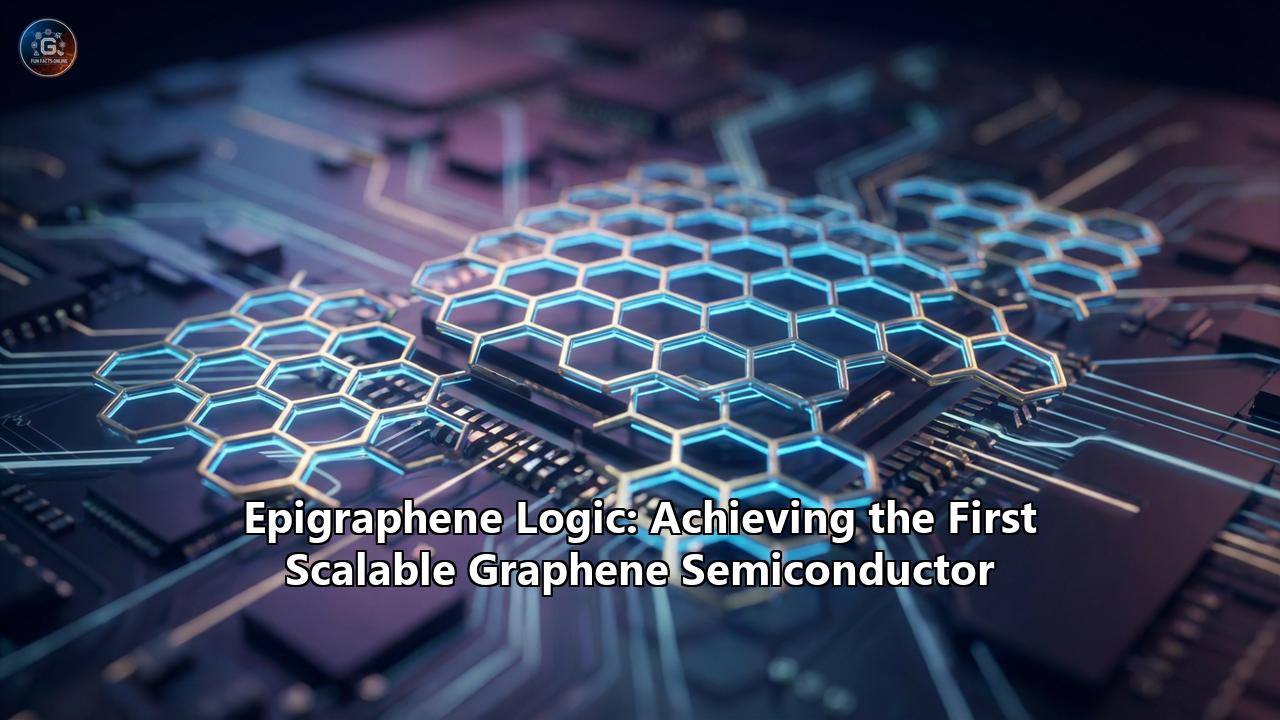
This is not just another incremental update to Moore’s Law; it is the dawn of Epigraphene Logic.
This comprehensive guide explores the science, the struggle, and the revolutionary future of this new material. We will journey from the atomic lattice of carbon to the terahertz processors of tomorrow, dissecting how this breakthrough was achieved and why it signals the end of the Silicon Age.
Part 1: The Silicon Stalemate and the Carbon Dream
To understand the magnitude of Epigraphene Logic, we must first understand the crisis it solves.
The Red Brick Wall
For 60 years, the digital world has been built on silicon. It is cheap, abundant, and possesses a natural "bandgap"—an energy hurdle that electrons must jump over to conduct electricity. This allows silicon to act as a switch (a transistor), turning current on (1) and off (0). This binary switching is the fundamental language of all logic, from the calculator in your pocket to the supercomputers training AI.
But silicon is tired. As we shrink transistors to just a few nanometers, we face three insurmountable problems:
- Heat: Pushing electrons through silicon generates resistance, which creates heat. At billions of operations per second, chips are becoming hotplates that require massive cooling systems.
- Speed Limits: Silicon electrons are relatively heavy and slow. We are struggling to push clock speeds past 5–6 GHz without melting the chip.
- Quantum Leakage: At the atomic scale, electrons in silicon stop behaving like particles and start tunneling through barriers, causing "leakage" currents that drain battery life even when the device is off.
The Graphene Promise
Enter graphene. Isolated in 2004, this single layer of carbon atoms arranged in a honeycomb lattice is the strongest material known to man. But its electrical properties are what seduced physicists.
- Mobility: Electrons in graphene behave like "massless Dirac fermions," moving 10 to 100 times faster than in silicon.
- Thermal Conductivity: It dissipates heat better than copper.
- Durability: It is chemically inert and mechanically robust.
If you could build a computer out of graphene, it would run at Terahertz (THz) speeds—1,000 times faster than today's best CPUs—while running cool.
The Bandgap Problem: Why Graphene Failed for 20 Years
So, why don't we have graphene computers? Because natural graphene is a semimetal, not a semiconductor. It has no bandgap. In simple terms, a graphene transistor is like a light switch that is permanently stuck in the "ON" position. You can flow current through it beautifully, but you cannot stop it. Without the ability to switch off, you cannot create the 0s and 1s required for digital logic.
For two decades, scientists tried to force a bandgap into graphene. They cut it into tiny ribbons, crumpled it, and doped it with chemicals. But every time they managed to open a bandgap, they destroyed the very thing that made graphene special: its high electron mobility. The "on" state became slow and sluggish. It seemed like a zero-sum game.
Until the Epigraphene Lab changed the rules.
Part 2: The Breakthrough – Semiconducting Epigraphene (SEG)
The solution didn't come from forcing graphene to be something it isn't; it came from growing it in a completely new way. The breakthrough lies in a material called Semiconducting Epigraphene (SEG).
What is Epigraphene?
"Epigraphene" is short for epitaxial graphene. "Epitaxy" refers to the growth of a crystal layer on top of another crystal, where the new layer aligns perfectly with the atomic structure of the substrate.
The team at Georgia Tech, collaborating with Tianjin University, used Silicon Carbide (SiC) as the substrate. SiC is a tough, crystalline compound used in high-power electronics (like EV chargers) and sandpaper.
When you heat Silicon Carbide to extremely high temperatures (over 1,300°C) in a vacuum, the silicon atoms on the surface sublime (evaporate), leaving the carbon atoms behind. These leftover carbon atoms self-assemble into graphene.
The Magic of the "Buffer Layer"
Usually, when graphene grows on SiC, the first layer—called the buffer layer—is chemically bonded to the silicon carbide underneath. Because it's tied down by these bonds, it can't conduct electricity. It’s an insulator. Researchers typically ignored this layer, focusing on the second layer that grows on top, which is free-floating and conductive (but has no bandgap).
Walter de Heer and his team asked a different question: What if we could engineer this buffer layer?
They developed a precise method called Confinement Controlled Sublimation (CCS). By controlling the rate at which silicon evaporated, they created a pristine, single-crystal buffer layer that was perfectly aligned with the SiC substrate.
Here is the twist: When grown this perfectly, the buffer layer IS a semiconductor.
The chemical bonds between the carbon layer and the silicon carbide substrate create the elusive bandgap (0.6 electron volts) naturally, without destroying the crystal structure.
The Numbers That Shocked the World
The resulting material, SEG, boasts metrics that outperform every other candidate for post-silicon electronics:
- Bandgap: 0.6 eV. (Perfect for digital logic; large enough to switch off, small enough to switch on easily).
- Electron Mobility: Over 5,000 cm²/Vs. (For comparison, silicon is around 500 cm²/Vs. This means SEG is 10 times faster).
- On/Off Ratio: The transistors achieved a switching ratio of 10,000 to 1. This is the "logic" capability. It can definitively distinguish between a 0 and a 1.
This was the first time anyone had created a graphene-based material that could act as a true transistor while retaining the "superhighway" speeds of carbon.
Part 3: The Physics of Epigraphene Logic
How does Epigraphene Logic actually work? It differs fundamentally from the silicon logic we use today.
Ballistic Transport: The Electronic Bullet Train
In a silicon chip, an electron moving from the source to the drain is like a car driving through heavy traffic. It constantly bumps into atoms, impurities, and other electrons. These collisions (scattering) slow it down and generate heat. This is "diffusive transport."
Epigraphene enables ballistic transport. Because the carbon lattice is so perfect and the electrons interact with it so smoothly, they fly through the material like bullets through a vacuum. They don't scatter. They don't generate friction.
This means a logic gate made of SEG can switch states almost instantaneously. The theoretical limit isn't in the Gigahertz (billions of cycles per second) but in the Terahertz (trillions of cycles per second).
The Edge State: A Quantum Bonus
The researchers discovered something else remarkable: the Epigraphene Edge State.
When you cut a ribbon of this material, the edges behave differently than the middle. Electrons at the edges form a "protected" quantum state where they can travel for millimeters without any resistance—literally zero. This is similar to the behavior seen in superconductors or fiber optics, but for electrons.
This "edge state" transport is robust against disorder. Even if the edge is a little rough, the electrons just glide over the bumps. This property could allow for "interconnects" (the wires connecting transistors) that consume zero energy, solving one of the biggest power drains in modern chips.
Part 4: Manufacturing – Why This Is Scalable
The graveyard of material science is filled with "miracle materials" that only work in a pristine lab environment or require gold-plated equipment. Carbon Nanotubes, for example, are amazing but impossible to align by the billion.
Epigraphene Logic is different because it was designed with manufacturability in mind.
The Silicon Carbide Advantage
The substrate, Silicon Carbide (SiC), is already an industrial standard.
- Existing Supply Chains: We already mass-produce SiC wafers for the electric vehicle industry (used in Teslas and other EVs for power conversion).
- Standard Sizes: The researchers demonstrated the process on industry-standard wafer chips.
- Compatibility: The tools used to etch, pattern, and gate Epigraphene are the same lithography tools (e-beam, UV lithography) used in Intel or TSMC fabs today.
The CCS Process (Confinement Controlled Sublimation)
The "secret sauce" is the furnace method.
- Sandwich Technique: Two SiC chips are stacked face-to-face.
- Vacuum Heating: They are placed in a graphite crucible and heated to ~1,600°C.
- Controlled Leak: A tiny leak in the crucible controls the rate at which silicon atoms escape. This "confinement" ensures that the carbon atoms rearrange themselves slowly and perfectly, rather than bubbling up chaotically.
This process yields "terraces" of graphene that are atomically flat and defect-free over large areas. This uniformity is critical for making chips with billions of identical transistors.
Part 5: Applications of Epigraphene Logic
If we successfully transition to Epigraphene Logic, what does the world look like?
1. Terahertz Computing
Current computers clock out around 5 GHz. A Terahertz computer would be 1,000 times faster.
- Real-time AI: Large Language Models (LLMs) like GPT-4 could run locally on your phone, training and inferring instantly without needing a data center.
- Instant Simulation: Weather modeling, drug discovery, and physics simulations that take months on supercomputers could be done in hours.
2. The "Cold" Chip
Because of the high mobility and low resistance, Epigraphene chips would run incredibly cool.
- Green Data Centers: Currently, data centers consume nearly 2% of the world's electricity, much of it just for air conditioning. Epigraphene could slash this energy footprint.
- Battery Life: Your smartphone could last for weeks, not days.
3. High-Frequency Wireless (6G and Beyond)
Terahertz frequencies are the frontier of wireless communication (6G). Silicon struggles to generate or detect these signals. Epigraphene transistors are naturally tuned to these frequencies.
- Epigraphene logic could be the backbone of 6G base stations, enabling wireless speeds that rival fiber optics (1 Terabit/second wireless).
4. Quantum Computing Interface
Epigraphene's quantum properties (specifically the edge states) make it a prime candidate for Topological Quantum Computing. Unlike the fragile qubits of today that need near-absolute zero temperatures, Epigraphene's quantum states are robust at higher temperatures. It could serve as the bridge between classical logic and quantum processors.
Part 6: The Road Ahead – Challenges and Timeline
Is this happening tomorrow? No. We are at the "Wright Brothers" stage. The plane flies, but we aren't crossing the Atlantic yet.
Challenge 1: The Dielectric
To make a transistor, you need a "gate"—a layer of insulation on top of the semiconductor that controls the flow of current. Silicon has a perfect natural insulator: Silicon Dioxide. Graphene does not.
Researchers need to find a dielectric material that can be deposited on top of Epigraphene without damaging its delicate atomic structure. Currently, they are experimenting with Boron Nitride and Aluminum Oxide, but perfecting this interface is crucial for reliability.
Challenge 2: P-Type vs. N-Type
Logic circuits (CMOS) require two types of transistors: N-type (carries negative electrons) and P-type (carries positive "holes"). The current breakthrough successfully demonstrated N-type behavior. Developing a matching P-type Epigraphene transistor that performs just as well is the next major hurdle for building complex logic gates like NAND or NOR.
Challenge 3: Cost
While SiC wafers are available, they are significantly more expensive than silicon wafers. Epigraphene chips will likely appear first in high-value applications (military, space, high-frequency trading, supercomputing) before trickling down to consumer electronics.
Timeline
- Now: Functional prototype transistors and basic logic gates.
- 3-5 Years: Small-scale integrated circuits (thousands of transistors) for specialized RF (Radio Frequency) applications.
- 10 Years: Commercial logic chips competing with high-end silicon.
- 15+ Years: Widespread adoption as the standard for post-silicon electronics.
Conclusion: A New Paradigm
For 50 years, we have been refining the stone age of computing—literally etching circuits into silicon stone. We have polished that stone until we hit the atoms.
Epigraphene Logic is not just a polish; it is a new material age. It harnesses the carbon bond—the strongest bond in nature—to carry information faster and more efficiently than ever thought possible.The "Red Brick Wall" has not just been broken; it has been dissolved. We are no longer limited by the sluggishness of silicon or the heat of resistance. The era of Carbon Electronics has officially begun, and the logic of the future will be written on a sheet of atoms one layer thick.
Reference:
- https://bits-chips.com/article/graphene-may-challenge-silicon-after-all/
- https://www.msesupplies.com/blogs/news/the-future-of-electronics-graphene-semiconductors
- https://research.gatech.edu/feature/researchers-create-first-functional-semiconductor-made-graphene
- https://nano.swiss/news/researchers-claim-first-functioning-graphene-based-chip
- https://news.ycombinator.com/item?id=38878780
- https://eepower.com/tech-insights/researchers-create-worlds-first-graphene-semiconductor/
- https://falling-walls.com/breaking-silicon-barrier-walt-de-heers-semiconducting-graphene-innovation
- https://www.quora.com/Semiconductors-What-are-the-problems-preventing-graphene-to-hit-markets-1
- https://www.researchgate.net/figure/Demonstration-of-the-1-G0-edge-state-a-b-Sample-S2-axis-along-ZZ-orientation-width-1_fig3_366400623
- https://www.flywing-tech.com/blog/researchers-create-worlds-first-graphene-semiconductor/
- https://www.researchgate.net/publication/369240676_Ultrahigh_mobility_semiconducting_epitaxial_graphene_on_silicon_carbide