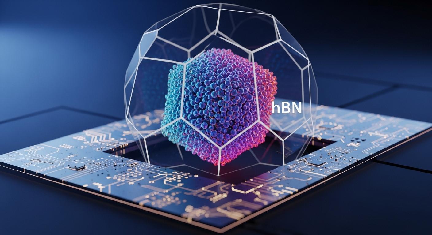
The quest for understanding and manipulating magnetism at its most fundamental level has driven a revolution in nanoscale sensing. At the forefront of this exploration are 2D quantum materials, which offer unprecedented sensitivity and spatial resolution. Among these, hexagonal boron nitride (hBN) has emerged as a remarkable platform, heralding a breakthrough in nanoscale vectorial magnetometry – the ability to measure not just the strength but also the precise direction of magnetic fields in incredibly small volumes. This development promises to unlock new frontiers in fundamental physics, materials science, and biomedical imaging.
The Nanoscale Magnetometry Challenge
Measuring magnetic fields at the nanoscale is crucial for unraveling the mysteries of novel magnetic materials, understanding spin transport in spintronic devices, and even imaging the faint magnetic signatures of biological processes. Traditional magnetometry techniques often lack the sensitivity or the spatial resolution required to probe these delicate nanoscale phenomena. While quantum sensors, such as the nitrogen-vacancy (NV) center in diamond, have made significant strides, they come with their own set of limitations. NV centers, for instance, are inherently single-axis sensors, meaning they can only measure the component of the magnetic field along one specific direction. Furthermore, their performance can be compromised by strong magnetic fields not aligned with this axis, and their three-dimensional nature can limit how close they can get to a sample, thereby restricting spatial resolution.
Enter 2D Quantum Materials: A New Paradigm
Two-dimensional materials, with their atomically thin structures, offer a natural advantage for nanoscale sensing. They can be brought into extremely close proximity with a sample, potentially achieving atomic-scale spatial resolution. Hexagonal boron nitride, often dubbed "white graphene" due to its similar honeycomb lattice structure, has rapidly gained prominence in the realm of quantum technologies. Its wide bandgap, unique optical and spin properties, and ability to host stable quantum emitters make it an ideal candidate for quantum sensing applications.
The hBN Breakthrough: Spin Defects Take Center Stage
The key to hBN's prowess in magnetometry lies in its atomic-scale imperfections, or "spin defects." These defects, such as the negatively charged boron vacancy (VB-), act as tiny quantum sensors. These VB- defects possess an electron spin that can be initialized and read out using light, a technique known as optically detected magnetic resonance (ODMR). The energy levels of these spins are sensitive to external magnetic fields; by precisely measuring changes in the emitted light (photoluminescence) as microwaves are applied, researchers can determine the strength and orientation of the local magnetic field.
Recent groundbreaking work, notably by physicists at the University of Cambridge, has demonstrated that specific spin defects in hBN can overcome the limitations of previous quantum sensors. These hBN-based sensors are capable of vectorial magnetometry, meaning they can simultaneously measure both the magnitude and the direction of the magnetic field at the nanoscale and at room temperature. This is a significant leap forward, as it provides a much more complete picture of the magnetic environment.
Why hBN is a Game-Changer for Vectorial Magnetometry
Several factors contribute to hBN's success in this domain:
- Multi-Axis Sensing: Unlike the single-axis NV centers in diamond, certain carbon-related spin defects in hBN exhibit a low-symmetry structure. This low symmetry, combined with favorable excited-state dynamics, allows for the optical detection of magnetic resonances along multiple axes, enabling true vectorial field measurements.
- Broad Dynamic Range: hBN-based sensors can operate effectively over a much wider range of magnetic field strengths, even when the field is not perfectly aligned with a specific defect axis. This is a crucial advantage when studying materials that generate strong and arbitrarily oriented magnetic fields, such as ferromagnetic nanostructures. The ODMR contrast of some hBN defects can persist beyond 50 mT for arbitrarily oriented fields.
- Enhanced Spatial Resolution: Being a 2D material, hBN flakes can be exfoliated down to a few atomic layers. This allows the quantum sensor to be placed in extremely close proximity to the target sample, leading to spatial resolutions potentially governed by the fundamental sensor-sample distance – even approaching atomic scales. This intimate contact is difficult to achieve with bulk materials like diamond.
- Room Temperature Operation: The ability to perform these sensitive measurements at room temperature significantly broadens the range of potential applications and simplifies experimental setups.
- Versatility and Integration: hBN is relatively easy to work with and can be integrated with various other materials, including other 2D materials, to form van der Waals heterostructures. This opens up exciting possibilities for in situ quantum sensing and imaging of complex material systems and devices. Furthermore, techniques are being developed to create arrays of hBN quantum sensors with nanoscale accuracy, allowing for high-resolution magnetic field imaging. Researchers are also exploring fibre-integrated hBN sensors for remote sensing applications.
The Power of ODMR and Spin Defects
The operational principle behind these hBN sensors relies on optically detected magnetic resonance (ODMR). Spin defects in hBN, such as the VB- or certain carbon-related defects, can be optically polarized (their spins aligned) using a laser. Microwave radiation is then applied, and if its frequency matches the energy difference between spin states (which is affected by the external magnetic field), the spins will transition, leading to a change in the photoluminescence intensity. By sweeping the microwave frequency and monitoring the fluorescence, a spectrum is obtained that directly reflects the local magnetic field. Advanced ODMR techniques, including pulsed sequences like Rabi oscillations, Ramsey interference, and Hahn echo, further allow for the detailed investigation of spin properties and their interaction with the environment.
Researchers have successfully used these hBN spin defects to sense not only static magnetic fields and magnetic noise but also temperature, strain, nuclear spins, and even paramagnetic spins in liquids. The most well-studied VB- defect was first identified with ODMR in 2020 in neutron-irradiated hBN, and these defects have since been created using various methods like ion, electron, proton irradiation, and femtosecond laser writing. More recently, a carbon-based defect (S=1) in hBN has shown great promise for vectorial magnetometry due to its low symmetry and advantageous excited-state dynamics, exhibiting high DC sensitivity and a broad dynamic range. Another newly discovered carbon-based defect with a spin-half system offers the potential for omnidirectional magnetometry with no blind spots. This diversity of defects and their unique properties expand the toolkit for quantum sensing with hBN.
Pushing the Boundaries: Latest Advances and Future Outlook
The field is rapidly evolving. Recent research published in Nature Communications (May 2025) by the Cambridge team highlights the capabilities of carbon-related spin defects in hBN for vectorial magnetometry, emphasizing the role of low symmetry and favorable excited-state optical rates in achieving a large dynamic range and vectorial sensing. They demonstrated sub-µT/√Hz DC magnetic field sensitivity, even for off-axis bias magnetic fields exceeding 50 mT. Other research focuses on enhancing the coherence times of hBN spin defects, which is crucial for improving sensitivity, particularly for AC magnetometry. Dynamical decoupling techniques have been shown to extend coherence times by orders of magnitude.
Furthermore, efforts are underway to improve the fabrication and control of these quantum sensors. This includes developing methods for wafer-scale production of hBN thin films with controlled thicknesses and optimized ODMR properties, which is essential for advancing practical applications. Studies are exploring the ODMR characteristics of hBN films grown by different methods like MOCVD, CVD, and MBE, and the impact of post-growth annealing. The ability to precisely position sensor spots with nanoscale accuracy using techniques like helium ion microscopy is also paving the way for high-resolution magnetic field imaging.
The potential applications are vast:
- Fundamental Physics: Probing exotic magnetic phases in 2D materials and other quantum materials.
- Materials Science: Characterizing magnetic domains, current flow in nanoelectronic and spintronic devices, and understanding superconductivity.
- Nanoscale Imaging: Achieving unprecedented spatial resolution in magnetic field mapping.
- Biomedical Applications: While still an area of active research, the potential for high-sensitivity, biocompatible magnetic sensors opens doors for studying biological systems, though brightness of some hBN defects compared to NV centers is a factor to consider for deep tissue applications. However, hBN's 2D nature and potential for close proximity sensing could be advantageous for surface-based biological sensing.
- Integrated Quantum Devices: The compatibility of hBN with nanofabrication techniques suggests the integration of these sensors into complex quantum circuits and hybrid devices.
Challenges and the Path Forward
Despite the exciting progress, challenges remain. Optimizing the creation and placement of specific spin defects with desired properties is an ongoing area of research. Understanding and mitigating sources of noise and decoherence are crucial for pushing sensitivity limits further. Further research is also needed to fully understand the atomic and electronic structure of all relevant defects and to improve their stability and brightness. The variability in optical rates observed across different defects, while potentially offering tuning capabilities, also presents a challenge for consistency.
Nevertheless, the hBN breakthrough in nanoscale vectorial magnetometry represents a monumental stride. By addressing critical limitations of existing technologies and offering unparalleled spatial resolution due to its 2D nature, hBN is poised to become a cornerstone material in the field of quantum sensing. As research continues to refine these remarkable sensors and explore new applications, the scientific community eagerly anticipates the wealth of discoveries and innovations they will undoubtedly unlock. The journey into the quantum realm of magnetism, with hBN as our guide, has just become significantly more illuminating.