The Future is Forged in Light: How Silicon Photonics is Revolutionizing Data Transmission
In the heart of our digital world, from the sprawling data centers that power the cloud to the supercomputers unraveling the universe's secrets, a fundamental bottleneck looms. For decades, the relentless march of Moore's Law has packed ever-more processing power onto silicon chips. Yet, the humble copper wire, the workhorse of electronic communication for over a century, is struggling to keep pace. As data rates soar and the demand for instantaneous information becomes insatiable, the physical limitations of using electrons to shuttle data are creating a traffic jam on the information superhighway. The heat generated, the power consumed, and the signal degradation over distance are all symptoms of a technology reaching its physical limits.
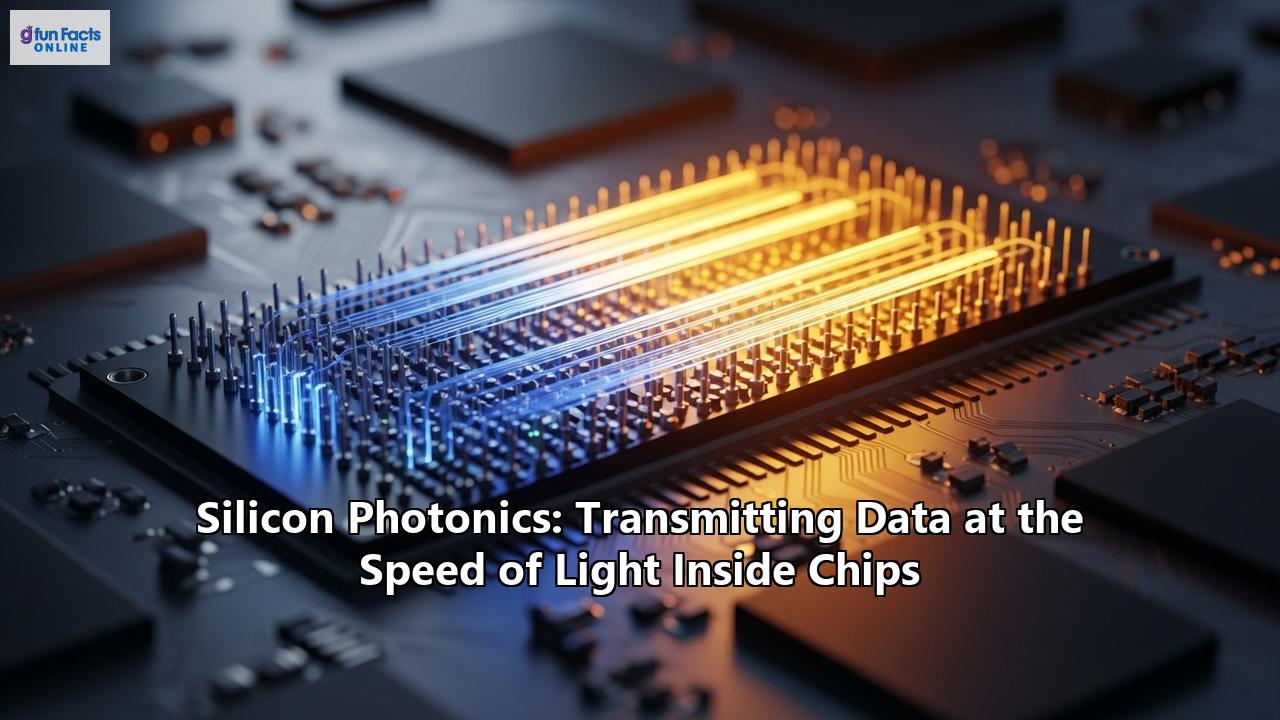
Enter a revolutionary technology poised to shatter this bottleneck: silicon photonics. This groundbreaking field is not about creating better transistors, but about fundamentally changing the way data travels within and between chips. It’s a paradigm shift from electrons to photons—particles of light. By transforming silicon, the very foundation of the modern electronics industry, into an optical medium, silicon photonics enables the transmission of data at the speed of light. This is achieved by creating miniature optical circuits, known as photonic integrated circuits (PICs), directly on a silicon wafer. These PICs can guide, modulate, and detect light, allowing for the creation of ultra-fast, low-power, and highly integrated optical interconnects that promise to redefine the future of computing, communication, and beyond.
The core idea is to replace electrical wires with optical waveguides—tiny channels etched into silicon that act as "light pipes." This transition promises orders-of-magnitude improvements in bandwidth and energy efficiency, addressing the twin crises of data deluge and power consumption that threaten to stall technological progress. By leveraging the multi-trillion-dollar infrastructure of the existing semiconductor industry, silicon photonics offers a scalable and cost-effective path to manufacturing these advanced optical systems. This isn't just a simple replacement of one wire for another; it's a deep integration of light and electronics on a single chip, a fusion that will power the next generation of artificial intelligence, enable continent-spanning quantum networks, and even bring sophisticated medical diagnostics into our homes.
The Dawn of a New Interconnect: Why Light is the Answer
The modern world runs on data, and the amount of data we generate, process, and move is growing at an exponential rate. This explosion, fueled by AI, cloud computing, and the Internet of Things (IoT), has pushed traditional copper interconnects to their breaking point. Several fundamental physical limitations of using electrons to transmit information over copper wires become increasingly problematic at high speeds and over longer distances.
Firstly, copper wires suffer from frequency-dependent loss, meaning the signal degrades more significantly as the data rate (frequency) increases. This attenuation limits both the speed and the distance over which data can be reliably transmitted. To compensate, more power is needed to boost the signal, which in turn generates more heat—a major issue in densely packed servers and data centers. It is estimated that data centers already account for a significant portion of global electricity consumption, and the power required for data movement is a major contributor. Silicon photonics directly addresses this by using photons, which travel through optical waveguides with minimal loss and are not bound by the resistive properties of copper. This allows for data transmission over much longer distances—from millimeters on a chip to kilometers between data centers—with significantly lower power consumption.
Secondly, copper interconnects are susceptible to electromagnetic interference (EMI) and crosstalk, where signals in adjacent wires interfere with each other. As the density of interconnects increases, this "noise" becomes a major challenge, corrupting data and limiting bandwidth. Optical signals, on the other hand, are immune to EMI. Photons in different waveguides do not interact with each other, allowing for incredibly dense and clean data transmission pathways.
The combination of these factors creates what is often called the "power wall," where the energy required to move data off-chip begins to exceed the power budget of the entire package. Silicon photonics offers a way to break through this wall. By transmitting data using light, it offers:
- Massive Bandwidth: A single optical fiber can carry tens of terabits per second by using techniques like Wavelength Division Multiplexing (WDM), where different colors (wavelengths) of light each carry a separate data channel. This provides a monumental increase in data-carrying capacity compared to an electrical cable.
- Lower Power Consumption: Transmitting a bit of data using photons requires significantly less energy than using electrons, especially over distance. This translates to lower electricity bills, reduced heat generation, and a smaller carbon footprint for large-scale computing operations.
- Longer Reach: Optical signals can travel kilometers with minimal degradation, whereas high-speed electrical signals are often limited to just a few meters before needing re-timing and amplification, adding latency and power overhead.
- Reduced Latency: By enabling faster and more direct communication paths, optical interconnects can lower the time it takes for data to travel between processors, memory, and storage, which is critical for applications like high-performance computing and real-time AI.
In essence, as the internal components of chips have become blindingly fast, the connections between them have become the bottleneck. Silicon photonics unshackles the system by replacing the congested copper "streets" with a multi-lane, light-speed "highway."
The Building Blocks of Light: Anatomy of a Silicon Photonic Circuit
At its core, a silicon photonic integrated circuit (PIC) is an intricate system of microscopic components designed to generate, guide, manipulate, and detect light, all fabricated on a silicon chip. These components are the optical equivalents of the resistors, capacitors, and transistors that form a traditional electronic circuit. The magic of silicon photonics lies in its ability to manufacture these diverse optical elements using the same high-volume, high-precision complementary metal-oxide-semiconductor (CMOS) processes that have driven the electronics industry for half a century.
Most silicon photonic devices are built on a Silicon-on-Insulator (SOI) wafer. This structure consists of a thin layer of crystalline silicon sitting on top of a layer of silicon dioxide (glass), which in turn is on a standard silicon substrate. The significant difference in refractive index between silicon (around 3.5) and silicon dioxide (around 1.45) is the key. This high index contrast allows light to be tightly confined within the top silicon layer through a phenomenon called total internal reflection, much like how light is guided down a fiber optic cable. This strong confinement enables the creation of incredibly small and efficient optical components.
The primary components that make up a typical silicon photonic circuit include:
1. Waveguides: Often called the "wires" of a PIC, waveguides are microscopic channels etched into the silicon layer that guide light from one component to another. Their design is critical for minimizing signal loss. Roughness on the waveguide sidewalls, a byproduct of the etching process, can cause light to scatter, leading to signal degradation. Therefore, advanced lithography and etching techniques are employed to create exceptionally smooth and precise waveguide structures. While silicon is the primary material, silicon nitride is also frequently used, as it offers lower optical loss and is transparent over a wider range of wavelengths, including visible light. 2. Modulators: A modulator is a crucial active component that encodes electrical data onto a beam of light. It acts as a high-speed optical shutter or phase shifter. The most common method for modulation in silicon is based on the free carrier plasma dispersion effect. By applying a voltage across a p-n junction integrated into the waveguide, the concentration of free charge carriers (electrons and holes) within the silicon can be rapidly changed. This change in carrier concentration alters the refractive index of the silicon, which in turn changes the phase or amplitude of the light passing through it.Two primary types of modulators dominate silicon photonics:
- Mach-Zehnder Modulator (MZM): In an MZM, the incoming light is split into two separate waveguides (the two "arms" of the interferometer). At least one arm has a phase shifter. By applying a voltage, a phase difference is created between the light in the two arms. When the arms recombine, the light waves interfere with each other. If they are in phase, they combine constructively, resulting in a strong output signal ("on" state). If they are out of phase, they interfere destructively, canceling each other out and resulting in a weak or no signal ("off" state). This on-off keying is how binary data is encoded.
- Ring Modulator: This compact device consists of a tiny "racetrack" or ring-shaped waveguide placed very close to a straight waveguide. At a specific wavelength, known as the resonant wavelength, light from the straight waveguide couples into the ring and circulates. By applying a voltage to a p-n junction in the ring, its refractive index is altered, shifting the resonant wavelength. This allows the modulator to switch from a state where light passes by unaffected (off-resonance) to a state where light is absorbed into the ring (on-resonance), effectively modulating the signal. Ring modulators are very compact and power-efficient but are also more sensitive to temperature variations and fabrication imperfections.
- External Laser Source: The simplest approach is to use a separate, high-performance laser made from a direct-bandgap material like Indium Phosphide (InP). The light from this external laser is then coupled onto the silicon photonic chip using specialized structures like grating couplers or edge couplers. While practical, this approach adds complexity, cost, and potential points of failure to the packaging process.
- Hybrid Integration: This more advanced technique involves bonding a thin sliver of III-V material (like InP) directly onto the silicon photonic wafer. The silicon waveguide circuit is then used to form part of the laser cavity, while the InP material provides the optical gain (the ability to generate light). This allows for the creation of high-performance lasers directly on the silicon platform, but it adds several complex steps to the fabrication process and can impact manufacturing yield and cost.
By combining these building blocks, engineers can create complex systems-on-a-chip that perform sophisticated data transmission and processing functions, all driven by the speed of light.
Powering the Digital Universe: Key Applications of Silicon Photonics
The ability to move massive amounts of data quickly and efficiently is the lifeblood of the modern digital economy. Silicon photonics is rapidly becoming the critical enabling technology across a diverse range of applications, from the engines of the internet to the sensors in next-generation vehicles and the foundations of revolutionary new computing paradigms.
Data Centers and Telecommunications: The High-Bandwidth Backbone
The most mature and economically significant application for silicon photonics today is in data centers and telecommunications networks. Every search query, video stream, and cloud transaction translates into data that must be shuttled between servers, switches, and racks within a data center. As network speeds have escalated from 100G to 400G, and now to 800G and emerging 1.6T standards, copper interconnects have become a bottleneck due to their distance limitations and high power consumption.
Silicon photonic transceivers—compact modules that convert electrical signals to optical and back again—are now being deployed at massive scale. By integrating lasers, modulators, multiplexers, and detectors onto a single chip, these transceivers drastically reduce the cost, size, and power consumption compared to traditional solutions built from discrete optical components. This allows data center operators to increase bandwidth and port density, packing more communication capacity into the same physical space while controlling spiraling energy costs.
Looking forward, the trend is towards even tighter integration. Co-Packaged Optics (CPO) is an emerging architecture where the optical I/O chiplets are placed on the same package substrate as the main processing chip (like a network switch ASIC or a GPU). This dramatically shortens the electrical distance the data has to travel, from tens of centimeters on a motherboard to just a few millimeters within the package, leading to a substantial reduction in I/O power (by 30-50% or more) and latency. CPO is seen as essential for future scaling of network switches beyond 51.2 Tbps and for building the massive, interconnected systems required for large-scale AI.
High-Performance Computing (HPC)
In the world of supercomputing, performance is often limited not by the raw processing power of the compute nodes, but by the interconnects that link them together. HPC workloads, such as climate modeling, scientific simulations, and financial analysis, require massive parallel processing across thousands of nodes. Silicon photonics provides the high-bandwidth, low-latency fabric needed to keep all these processors fed with data, enabling faster communication and more efficient parallel computing. It can be used for rack-to-rack interconnects as well as for memory and storage acceleration, allowing for disaggregated architectures where pools of processing, memory, and storage can be dynamically configured and connected with optical links.
Artificial Intelligence and Machine Learning (AI/ML) Accelerators
The training and inference of large AI models, such as the large language models (LLMs) behind generative AI, are incredibly computationally intensive. This has created an insatiable demand for more powerful and efficient hardware. Silicon photonics is emerging as a revolutionary technology for AI acceleration, not just for communication, but for computation itself.
By arranging modulators and waveguides into specific architectures, photonic integrated circuits can perform the mathematical core of many AI algorithms—matrix-vector multiplications—entirely in the optical domain. Light representing the input data is passed through a network of optical components that have been programmed to represent the weights of a neural network. The resulting light intensity at the output detectors corresponds to the result of the multiplication, performed literally at the speed of light and with potentially far greater energy efficiency than electronic GPUs. This field of "photonic computing" promises to create a new class of AI accelerators that can overcome the energy and performance scaling challenges of current electronic hardware, paving the way for more powerful and sustainable AI systems.
LiDAR and Automotive Sensing
Light Detection and Ranging (LiDAR) is a cornerstone technology for autonomous vehicles, providing a real-time, 3D map of the car's surroundings. Traditional LiDAR systems are often bulky, mechanical, and expensive, using spinning mirrors to steer a laser beam. Silicon photonics offers a path to solid-state LiDAR on a chip.
By integrating all the necessary optical components—including lasers, beam steering elements (optical phased arrays), and detectors—onto a single silicon chip, LiDAR systems can be made vastly smaller, more robust, and less expensive to manufacture. This is particularly true for Frequency-Modulated Continuous-Wave (FMCW) LiDAR, a technique that not only measures distance but also the velocity of objects, a key advantage for safety. The continuous-wave nature of FMCW lasers makes them more amenable to on-chip integration compared to the high-peak-power pulsed lasers used in traditional time-of-flight systems.
Quantum Computing
One of the most futuristic and potentially transformative applications of silicon photonics is in quantum computing. Several leading approaches to building a fault-tolerant quantum computer rely on photons as qubits (quantum bits). Silicon photonics provides a perfect platform for building the complex optical circuits needed to generate, manipulate, and measure these photonic qubits.
Companies like PsiQuantum are leveraging standard semiconductor fabrication facilities to manufacture silicon photonic chips containing vast networks of single-photon sources, beam splitters, phase shifters, and detectors. The advantage of this approach is scalability. Because the chips can be mass-produced, it becomes feasible to build the large-scale, error-corrected systems, potentially requiring millions of qubits, that will be needed to solve commercially relevant problems. The stability and precision of lithographically defined circuits also provide a robust foundation for building reliable quantum processors.
Biosensors and Medical Diagnostics
The same properties that make silicon photonics great for communications also make it an incredibly sensitive platform for detecting biological and chemical substances. The basic principle involves creating a sensor, often a microring resonator, where a portion of the guided light (the evanescent field) extends outside the waveguide. The sensor surface is coated with antibodies or other molecules that are designed to capture a specific target biomarker (e.g., a virus protein or a cancer marker).
When the target biomarker binds to the surface, it slightly changes the local refractive index, which in turn causes a measurable shift in the resonant wavelength of the microring. This technique is extremely sensitive, label-free (meaning no fluorescent tags are needed), and can be highly multiplexed, with arrays of hundreds of sensors on a single chip, each designed to detect a different substance. This opens the door to low-cost, disposable "lab-on-a-chip" devices for a range of applications, including point-of-care medical diagnostics, at-home health monitoring, environmental sensing, and food safety testing.
The Path Forward: Overcoming Challenges and Embracing the Future
While the promise of silicon photonics is immense, the journey from laboratory demonstrations to widespread, cost-effective deployment is paved with significant technical hurdles. Overcoming these challenges is the central focus of researchers and engineers in the field today, and their solutions are shaping the future trajectory of the technology.
The Persistent Challenge of the Light Source
As previously mentioned, the inability of silicon to efficiently generate light remains the most fundamental obstacle. This has necessitated the use of heterogeneous integration, a sophisticated set of techniques for combining non-silicon materials with the silicon platform.
- Hybrid Integration: Bonding III-V materials like Indium Phosphide (InP) onto a fully processed silicon wafer allows for the fabrication of on-chip lasers and optical amplifiers. This approach is powerful but adds considerable complexity and cost to manufacturing, as it involves aligning and bonding two different material systems with high precision.
- External Laser Sources: Many current commercial products rely on high-performance, off-chip lasers that are precisely aligned and coupled to the silicon photonic chip during the packaging stage. While practical, this complicates the packaging process, increases the overall size and power consumption, and makes scaling to a large number of optical channels more difficult.
The "holy grail" remains a monolithic, electrically-pumped laser made from a CMOS-compatible material. Significant research is underway on germanium-on-silicon lasers, which leverage strain engineering and heavy doping to coax the material into emitting light more efficiently, but their performance still lags behind their III-V counterparts.
Manufacturing, Packaging, and Testing: The Bottlenecks of Scale
While leveraging CMOS foundries is a key advantage, fabricating photonic components is not the same as making transistors. Photonic devices are analog in nature and exquisitely sensitive to minute variations in fabrication.
- Manufacturing and Yield: Waveguides require nanometer-scale precision to minimize light scattering losses. The performance of devices like ring resonators can be significantly altered by tiny deviations in their dimensions, which can occur across a wafer. This makes achieving high yield—a high percentage of perfectly functioning chips per wafer—a major focus.
- Packaging and Alignment: Packaging is perhaps the biggest cost and throughput bottleneck in the industry today. Attaching optical fibers to the chip requires sub-micron alignment precision to ensure efficient light transfer. This is often a slow, active alignment process where the device is powered on and optimized in real-time, which is not scalable for high-volume manufacturing. Co-packaged optics (CPO) presents its own set of complex packaging challenges, requiring the integration of hot electronic ASICs with temperature-sensitive photonic chiplets in a single, reliable module.
- Cost: The high initial non-recurring engineering (NRE) costs for designing and creating the photomasks for a new chip, coupled with the expensive and often manual back-end packaging and testing processes, mean that the cost per chip is still relatively high, especially for lower-volume applications. Achieving the promised low costs of silicon photonics hinges on reaching massive production volumes to amortize these fixed costs, a classic chicken-and-egg problem for emerging applications.
Thermal Management: Keeping Cool Under Pressure
Silicon photonic devices are highly sensitive to temperature. The refractive index of silicon changes with temperature (the thermo-optic effect), which causes the operating wavelength of devices like filters and modulators to drift. A temperature change of just one degree Celsius can shift the resonant peak of a ring modulator enough to disrupt a communication channel.
Furthermore, active components like lasers, modulators, and electronic driver circuits all generate heat. In a densely integrated and co-packaged system, this heat can create significant on-chip temperature gradients and lead to thermal crosstalk, where heat from one component affects the performance of its neighbors. This necessitates sophisticated thermal management solutions, such as integrated heaters to fine-tune the temperature of individual components, thermoelectric coolers (TECs) to actively cool laser sources, and advanced heat sinks or microfluidic cooling channels to dissipate heat from the package. All of these solutions add to the power consumption and complexity of the system.
The Horizon of Innovation: Future Trends and Breakthroughs
Despite the challenges, the pace of innovation in silicon photonics is breathtaking. Researchers and industry leaders are charting a roadmap toward ever-higher performance, deeper integration, and new capabilities that will push the technology into even more applications.
- Co-Packaged Optics (CPO) and Beyond: The move from pluggable optical modules to co-packaged optics is a dominant trend, driven by the need to slash the power consumption of interconnects in data centers and HPC systems. Major players like Broadcom, Intel, and NVIDIA are heavily invested in CPO, with the first commercial 51.2T switches featuring CPO now emerging. The roadmap extends to 3D monolithic integration, where photonic and electronic layers could be vertically stacked, promising the ultimate in dense, low-power integration.
- Heterogeneous Integration and New Materials: The future of silicon photonics lies in becoming a truly versatile integration platform. Beyond just InP for lasers, researchers are integrating a host of novel materials to impart new functionalities that silicon lacks.
Thin-film lithium niobate (TFLN): This material possesses a strong electro-optic (Pockels) effect, enabling the creation of ultra-high-speed, low-loss modulators that far outperform their silicon counterparts.
Barium Titanate (BTO): Another material with an even stronger Pockels effect, BTO is being explored for extremely efficient modulators, particularly for applications in quantum photonics.
2D Materials: Graphene and other two-dimensional materials are being investigated for use in ultra-fast photodetectors and modulators.
Magnetic Materials: Integrating magneto-optic materials could allow for the fabrication of on-chip optical isolators—a critical component that prevents unwanted reflections from destabilizing lasers, which is currently a bulky, discrete part.
- AI-Driven Design and Optimization: The design of complex photonic circuits is becoming a major challenge. Artificial intelligence and machine learning are now being used to accelerate the design process, discover novel device structures, and even help optimize the performance of fabricated chips in real-time by controlling on-chip heaters and tuners.
- The Industry Landscape: The silicon photonics ecosystem is rapidly maturing, with a diverse range of players. Semiconductor giants like Intel, GlobalFoundries, and TSMC are providing foundry services for manufacturing. Networking leaders such as Cisco, Juniper Networks, and Broadcom are major consumers and developers of the technology, often through strategic acquisitions. A vibrant ecosystem of specialized design houses and innovative startups like Ayar Labs, Rockley Photonics, and PsiQuantum are pushing the boundaries in specific application areas like optical I/O, health sensing, and quantum computing, respectively. Research institutions like IMEC in Belgium and universities around the world continue to be hotbeds of fundamental innovation.
In conclusion, silicon photonics stands at the precipice of a new era. Having firmly established itself as the successor to copper in the high-stakes world of data centers, it is now branching out to revolutionize a host of other industries. The technology is moving beyond simple data pipes to become a platform for computation, sensing, and quantum information processing. The road ahead involves solving profound challenges in materials science, manufacturing, and thermal engineering. Yet, with a clear roadmap and a booming ecosystem of innovation, silicon photonics is no longer a futuristic promise. It is the solid-state foundation upon which the next generation of technology is being built—a future where data, and the world it powers, moves at the speed of light.
Reference:
- https://www.broadcom.com/info/optics/cpo
- https://www.mdpi.com/2072-666X/15/10/1211
- https://www.marketsandmarketsblog.com/emerging-trends-in-silicon-photonics-industry-shaping-the-future-of-data-and-connectivity.html
- https://www.photonics.intec.ugent.be/download/pub_3240.pdf
- https://institutionofelectronics.ac.uk/the-advent-of-co-packaged-optics-cpo-in-2025/
- https://www.signalintegrityjournal.com/articles/3648-idtechex-explores-emerging-materials-for-pics
- https://www.marketbusinessinsights.com/silicon-photonics-market
- https://www.ll.mit.edu/partner-us/available-technologies/heterogeneous-photonic-integration
- https://pubs.aip.org/aip/jap/article/130/7/070907/158219/Materials-for-emergent-silicon-integrated-optical
- https://www.i40today.com/co-packaged-optics-cpo-evaluating-different-packaging-technologies/
- https://www.latitudeds.com/post/silicon-photonics-in-2024-integrated-photonic-systems-roadmap
- https://www.futuremarketsinc.com/the-global-silicon-photonics-and-photonic-integrated-circuits-market-2025-2035/
- https://www.6wresearch.com/market-takeaways-view/10-promising-players-of-silicon-photonics-market-with-market-size
- https://tspasemiconductor.substack.com/p/from-taiwan-to-the-world-silicon
- https://www.marketsandmarkets.com/Market-Reports/silicon-photonics-116.html
- https://www.spiedigitallibrary.org/conference-proceedings-of-spie/11301/113010H/Heterogeneous-integration-of-III-V-based-photonics-with-silicon/10.1117/12.2548592.pdf
- https://hub.hku.hk/bitstream/10722/321971/1/content.pdf
- https://www.idtechex.com/en/research-report/co-packaged-optics/1019
- https://www.light-am.com/en/article/doi/10.37188/lam.2021.005
- https://www.marketsandmarkets.com/ResearchInsight/silicon-photonics-market.asp
- https://www.photonics.com/Articles/The-Integration-of-Materials-in-Photonic-Chips/a68803
- https://www.expertmarketresearch.com/blogs/top-silicon-photonics-companies
- https://www.idtechex.com/en/research-report/silicon-photonics-and-photonic-integrated-circuits-2024-2034-market-technologies-and-forecasts/1006
- https://arxiv.org/abs/2305.15820
- https://www.european-mrs.com/new-materials-photonics-emrs
- https://www.semanticscholar.org/paper/Roadmap-Roadmap-on-silicon-photonics-Thomson-Zilkie/2ce38845bdb685d10dd78fb90abe915c7be93252
- https://2024.sci-hub.se/5529/d0da500f4f45707a979855c3c0f40ed2/thomson2016.pdf
- https://www.mordorintelligence.com/industry-reports/silicon-photonics-market/companies