In the quiet, vibration-isolated cleanrooms of 2026, a profound shift is occurring in the race for the quantum computer. For decades, the dominant image of a quantum machine was a chandelier of gold and copper—a dilution refrigerator cooling superconducting circuits to near-absolute zero. But as the industry pushes past the 1,000-qubit barrier toward the holy grail of one million qubits, a new realization has taken hold: wires are the enemy.
The "wiring problem" is a fundamental thermodynamic and spatial bottleneck. You simply cannot thread millions of coaxial cables into a cryostat without turning it into an oven or running out of physical space. The solution, now driving the roadmaps of major players like PsiQuantum, QuEra, and Xanadu, is to abandon the wire for the photon.
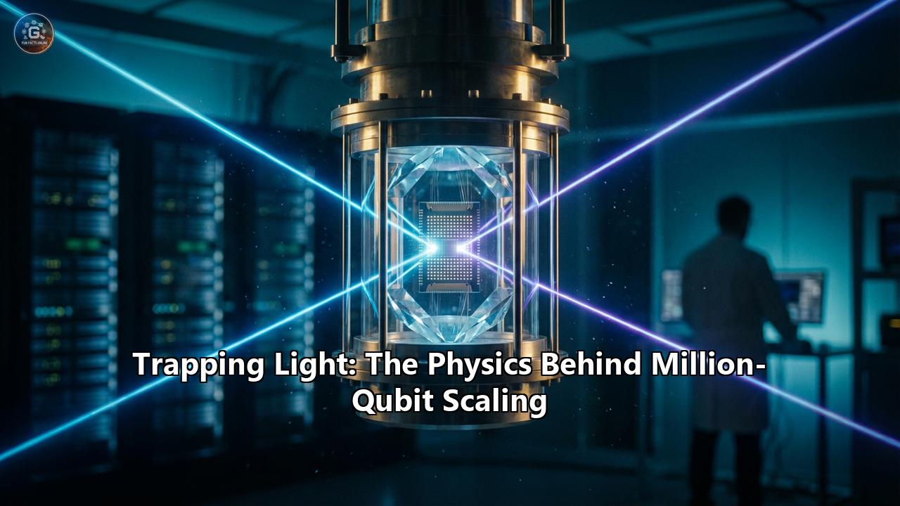
This is not merely about using light for communication. It is about a fundamental architectural inversion where light becomes the structural scaffolding of the computer itself. We are moving from the age of "trapping matter" to the age of "trapping light." This article delves into the deep physics—from the nanoscale wavefront engineering of metasurfaces to the quantum optics of fusion measurements—that is making the million-qubit era possible.
Part I: The Physics of the Container
To build a quantum computer with light, you must first master the art of holding it still, or at least confining it long enough to interact with matter. This was once thought impossible; light, by definition, wants to move at $c$. Two distinct physical breakthroughs—optical tweezers and high-Q cavities—have recently converged to solve this.
1.1 The Evolution of the Optical Trap: From Ashkin to Metasurfaces
The story begins with Arthur Ashkin at Bell Labs in the 1970s, who discovered that the momentum of light could exert a physical force. A focused laser beam creates a dipole force: dielectric particles are drawn toward the region of highest light intensity, much like a moth to a flame, but driven by the gradient of the electric field $\nabla |E|^2$.
For decades, generating these traps required bulky lenses and Spatial Light Modulators (SLMs). But to scale to a million atoms, you cannot rely on a million conventional lenses. The breakthrough, cemented by research groups like those at Columbia University in early 2026, lies in metasurfaces.
The Physics of Metasurfaces:A metasurface is a 2D array of sub-wavelength nanostructures—often silicon nanopillars—that act as discrete phase shifters. By varying the diameter and orientation of these nanopillars, engineers can imprint an arbitrary phase profile $\phi(x,y)$ onto an incoming plane wave.
- Wavefront Engineering: Instead of a curved glass lens refracting light, the metasurface delays the wavefront at each pixel to constructively interfere at a specific point in space (the focal point).
- The Scaling Factor: A single metasurface chip can now generate over 100,000 distinct, diffraction-limited focal spots from a single high-power laser beam. This replaces the "wiring" of control lines with a hologram of light. The physics here is non-trivial; it requires solving the inverse scattering problem to design a nanopillar map that minimizes crosstalk between adjacent traps, which are often separated by only a few micrometers.
1.2 The Optical Cavity: Modifying the Vacuum
While tweezers hold the atom in place, optical cavities are designed to hold the light around the atom. This is crucial for "readout"—getting information out of the qubit.
In free space, an atom emits a photon in a random direction (4$\pi$ steradians). Capturing this photon is inefficient. The solution is the Purcell Effect, a phenomenon where an optical cavity modifies the local density of optical states (LDOS).
- The Mechanism: By placing an atom inside a cavity with a high Quality Factor ($Q$) and small Mode Volume ($V$), you enhance the probability of the atom emitting a photon into the cavity mode by a factor $F_P \propto Q/V$.
- The Stanford Breakthrough (2026): Recent work has demonstrated arrays of silicon photonic crystal cavities that achieve this enhancement for hundreds of atoms simultaneously. The physics relies on "slow light" modes in the crystal, where the group velocity of light $v_g$ approaches zero, effectively trapping the photon near the atom long enough for a deterministic interaction. This allows for the simultaneous readout of thousands of qubits through a single fiber bundle, bypassing the wiring bottleneck.
Part II: The Matter-Light Interface
Light is excellent for transport, but poor for memory. Photons don't like to sit still. Therefore, the "million-qubit" machine is almost always a hybrid: a matter qubit (for memory) and a photonic qubit (for communication).
2.1 Neutral Atoms and "Erasure Conversion"
Companies like QuEra and Pasqal use neutral atoms (like Rubidium or Ytterbium) trapped in the optical tweezers described above. The physics of scaling these to millions of qubits relies on a specific quirk of atomic structure known as Erasure Conversion.
In a typical qubit, an error (a bit-flip or phase-flip) is a silent killer—you don't know it happened until your calculation fails. However, in atoms like Strontium-88 or Ytterbium-171, qubits can be encoded in metastable states.
- The Physics: When a high-energy "Rydberg" state decays (a common error source), it often falls into a specific "dark" ground state that is distinct from the computational $0$ and $1$ states.
- The Advantage: By periodically flashing the array with a probe laser, the system can see which atoms have fluoresced (decayed) and "flag" them as "erased" rather than "corrupted." In quantum error correction theory, an erasure error is infinitely easier to fix than a Pauli error because you know where it is. This physics allows neutral atom arrays to function with much lower fidelity thresholds, accelerating the path to fault tolerance.
2.2 Silicon Defects: The T-Center
Another approach, pursued by groups utilizing silicon photonics, involves "artificial atoms" trapped in the solid state. The T-center in silicon is a defect complex (two carbon atoms and a hydrogen atom) that acts as a spin-photon interface.
- Lattice Physics: The defect introduces localized electronic states within the silicon bandgap. Because silicon is the standard material of the semiconductor industry, T-centers can be integrated directly into the high-Q cavities mentioned earlier. The challenge here is phonon broadening—vibrations in the silicon lattice shaking the electron levels. Operating these systems requires ensuring that the "Zero Phonon Line" (ZPL)—the pure optical transition without vibrational noise—dominates the emission spectrum.
Part III: The Architecture of Light
How do you compute with a million qubits without a million control knobs? The answer lies in Fusion-Based Quantum Computing (FBQC), a radical architecture championed by PsiQuantum.
3.1 Measurement is Computation
In the standard "circuit model" (like IBM or Google), you keep qubits alive and apply gates to them. In FBQC, the qubits (photons) are flying through the system and are destroyed milliseconds after creation. The computation happens in the measurement.
The Physics of Type-II Fusion:The fundamental operation is the "fusion" measurement.
- Interference: Two photons, each from a separate entangled cluster, impinge on a Polarizing Beam Splitter (PBS).
- Indistinguishability: If the photons are identical in frequency, polarization, and arrival time (the Hong-Ou-Mandel effect), they interfere.
- The Measurement: Detectors at the output measure the polarization. Because of the quantum interference, certain detection patterns (e.g., "Horizontal" in detector 1 and "Vertical" in detector 2) project the remaining photons in the clusters into a new, larger entangled state.
- Teleportation: This process effectively "teleports" information and stitches small entangled resource states (created on-chip) into a massive, 3D "cluster state" that spans time and space.
3.2 The Paradox of Loss
The enemy of photonics is loss. If a photon scatters off a rough sidewall in a waveguide, the qubit is gone. This is where the Stabilizer Formalism of error correction shines.
In the FBQC model, a lost photon is just an "erasure." Because the 3D cluster state is highly redundant, the system can survive the loss of a significant percentage of its photons. The computation is like a bridge: you can remove random bricks (lost photons) and the bridge still stands, provided the "hole" (erasure) is identified.
Part IV: The Manufacturing Limits
The physics of scaling is ultimately the physics of manufacturing. To build a million-qubit machine, you need semiconductor foundries (like GlobalFoundries) to print these optical components.
4.1 Roughness and Scattering
The primary killer of optical coherence is sidewall roughness. When etching a silicon nitride waveguide, the lithography process leaves atomic-scale jaggedness.
- Rayleigh Scattering: This roughness scatters light proportional to $\sigma^2 / \lambda^4$, where $\sigma$ is the RMS roughness. For a quantum computer, even 0.1 dB/cm of loss can be fatal.
- The Fix: Modern "photonic damascene" processes and high-temperature hydrogen annealing are used to reflow the silicon, smoothing these atomic mountains into molehills, reducing scattering to negligible levels.
4.2 The Thermal Advantage
Unlike superconducting qubits, which require millikelvin temperatures ($<0.02$ K), photonic qubits operate at "warm" temperatures ($4$ K or even room temperature for some components). This changes the cooling physics entirely.
- Cooling Power: A dilution refrigerator has microwatts of cooling power at 10 mK. A standard cryocooler has watts of power at 4 K. This factor of $1,000,000\times$ in cooling capacity is exactly what allows the optical approach to scale. You can pump massive amounts of laser power (control signals) into the cryostat without boiling the qubits.
Part V: The Road to 2030
We are currently in the "utility-scale" transition.
- PsiQuantum is leveraging standard CMOS manufacturing to print millions of fusion gates, betting that the sheer volume of components will overcome individual error rates through massive redundancy.
- QuEra and Pasqal are scaling their optical tweezer arrays, using the "erasure conversion" physics to achieve fault tolerance with fewer physical atoms.
- Xanadu is pushing the "continuous variable" approach (squeezed light), where a single pulse of light carries multiple bits of information, increasing the information density per photon.
The physics of "trapping light" has moved from the Nobel-prize-winning curiosity of Arthur Ashkin to the industrial blueprint of the 21st century's most complex machine. By mastering the interaction of photons with metasurfaces, cavities, and defects, we are finally building a computer that runs not on electricity, but on the fundamental uncertainty of light itself.
Detailed Analysis of Key Technologies
1. Metasurface Optical Tweezers: The "Infinite" Switchboard
The traditional limit to scaling optical tweezers was the Space-Bandwidth Product (SBP) of the optical system. A standard microscope objective has a limited field of view where the focus is sharp. To trap 100,000 atoms, you would typically need a lens the size of a dinner plate, which is impractical for high-NA vacuum systems.
Metasurfaces break this limit. By dividing the aperture into sub-apertures or using "metalenses" that correct for aberrations (coma, astigmatism) at the nanostructure level, engineers can maintain a high Numerical Aperture (NA > 0.6) over a millimeter-scale field of view.- The Physics: Each nanopillar acts as a truncated waveguide. The phase shift $\phi$ acquired by light passing through a pillar of height $H$ and effective index $n_{eff}$ is $\phi = k_0 n_{eff} H$. By varying the pillar diameter, $n_{eff}$ changes, allowing 0 to $2\pi$ phase control.
- Impact: This allows for "sorting" atoms. If an atom is missing from a site (due to imperfect loading), the metasurface can generate a "tweezer conveyor belt"—moving a reserve atom into the empty slot in microseconds, ensuring a defect-free array.
2. The Photonic Interconnect: Entanglement Swapping
To reach a million qubits, you need modularity. A single chip cannot hold a million qubits. You need to connect chip A to chip B.
The Physics: This is done via Entanglement Swapping.- Ion A on Chip 1 emits a photon $\alpha$ entangled with its spin state.
- Ion B on Chip 2 emits a photon $\beta$ entangled with its spin state.
- Photons $\alpha$ and $\beta$ meet at a beamsplitter in the middle.
- A Bell State Measurement (BSM) on the photons projects Ion A and Ion B into an entangled state, even though they never interacted directly.
- Challenge: The photons must be indistinguishable. Any frequency shift (Doppler shift from the ion's motion) or polarization rotation in the fiber destroys the entanglement. This requires "frequency conversion" crystals—non-linear optical devices that change the photon's color to the telecom band (1550 nm) for low-loss transport without disturbing its quantum state.
3. Erasure Conversion in Neutral Atoms
The specific physics of Ytterbium-171 is worth a deeper look.
- The Level Structure: Yb-171 has a nuclear spin of 1/2 and no electronic spin in the ground state. The qubit is defined by the nuclear spin states.
- Rydberg Excitation: To perform a gate, the atom is excited to a Rydberg state ($n > 50$). This electron orbit is huge ($>100$ nm radius).
- The Error Mode: If the atom decays from the Rydberg state, it often falls into the ${}^3P_0$ or ${}^3P_2$ metastable states. These states are "dark" to the cooling light but can be detected by a separate "erasure" laser.
- Result: A "check" operation can be run mid-computation. "Is any atom in the metastable state?" If yes, that qubit is erased. The logical qubit (a group of physical atoms) notes the position of the hole and adapts its error correction code instantly. This improves the effective error threshold by nearly an order of magnitude.
Conclusion: The Light Age
The scaling to a million qubits is no longer a question of "if" but "how fast." The physics is established. We know how to trap atoms with holographic light. We know how to enhance their emission with cavities. We know how to stitch them together with fusion measurements.
The barrier is now engineering: characterizing the surface roughness of a waveguide to the angstrom, stabilizing a laser frequency to the Hz, and sorting 100,000 atoms before they decohere. But unlike the early days of quantum computing, these are challenges of execution, not discovery. The trap is set. The light is caught. The age of the photonic quantum computer has begun.