For over 50 years, the semiconductor industry has worshipped at the altar of Silicon. It is the bedrock of the modern world, the element that powered the digital revolution, from the first chunky mainframes to the smartphone in your pocket. But silicon is tired. As we shrink transistors down to the scale of mere atoms, pushing for faster AI and more powerful processors, silicon is hitting a physical wall. It is overheating. It is leaking energy. It is simply not fast enough anymore.
Enter Hyper-Mobile Germanium.
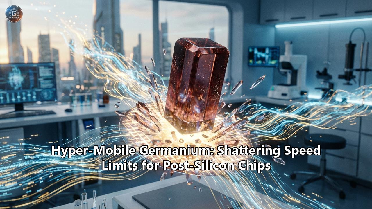
It sounds like science fiction, but it is actually a resurrection. Germanium was the material of the very first transistors in the 1940s before silicon took over due to its abundance and oxide stability. Now, thanks to a groundbreaking discovery announced in late 2025, germanium is back—and it has been supercharged. Researchers have engineered a new form of "strained" germanium that shatters the speed limits of electricity, offering a future where chips run cooler, faster, and with a fraction of the power.
This isn't just an incremental update; it is a rewriting of the rules of electron transport.
The 7.15 Million Breakdown: A New Speed Record
To understand why this is revolutionary, we have to talk about "mobility." In the world of semiconductors, mobility is the speed limit. It measures how quickly an electrical charge (either an electron or a "hole," which is the absence of an electron acting like a positive charge) can move through a material when a voltage is applied.
Standard silicon has a hole mobility of about 450 cm²/Vs (centimeters squared per volt-second). It’s decent, reliable, but unexciting—like a family sedan.
In December 2025, a team from the University of Warwick and the National Research Council of Canada stunned the physics world. They didn’t just beat silicon; they lapped it thousands of times over. They demonstrated a hole mobility of 7.15 million cm²/Vs in a new material called compressively strained germanium-on-silicon (cs-GoS).
To put that in perspective: if silicon is a person walking down the street, this new hyper-mobile germanium is a fighter jet screaming past at Mach 10.
How Did They Do It? The Atomic Corset
The secret lies in strain engineering. Imagine a layer of germanium atoms. Left alone, they sit comfortably in a crystal lattice. But if you grow that germanium on top of a silicon lattice, the atoms don't match up perfectly. The germanium atoms are naturally larger. To fit onto the silicon "floor," the germanium atoms have to squeeze together.
This "squeeze" acts like an atomic corset. It applies massive compressive strain to the germanium layer. This pressure drastically alters the quantum mechanical properties of the material. It smooths out the energy bumps that usually slow down charge carriers, creating a near-frictionless highway for electricity.
Critically, the researchers achieved this in a way that is silicon-compatible. They grew this nanometer-thin layer of super-germanium directly on a standard silicon wafer. This means the trillion-dollar semiconductor manufacturing industry doesn't have to throw away its factories; it can upgrade them.
The "Hole" Picture vs. The Electron Problem
In a modern computer chip (CMOS), you need two types of switches to make logic work:
- n-channel (NMOS): Uses electrons (negative charge) to carry current.
- p-channel (PMOS): Uses holes (positive charge) to carry current.
Historically, "holes" are the sluggish ones—the slow lane of the highway. This has always been a bottleneck. The record-breaking 7.15 million mobility number specifically applies to holes. This is a game-changer because it turns the traditionally slow p-channel into the fastest part of the chip.
But what about the electrons?
While compressive strain supercharges holes, a different trick is needed for electrons. This is where Germanium-Tin (GeSn) comes into play. By adding tin to germanium, or by pulling the atoms apart (tensile strain) rather than squeezing them, researchers are creating complementary "hyper-mobile" n-channels.
Recent data shows that Germanium-Tin transistors can achieve electron mobility 2.5 times higher than pure germanium. The vision for the chip of 2030 is a hybrid architecture: vertical transistors where p-channels are made of ultra-fast strained germanium and n-channels are made of high-speed germanium-tin, all sitting on a silicon base.
The Quantum Leap: Spin, Speed, and Control
Hyper-mobile germanium isn't just about making your phone faster; it is a key that unlocks quantum computing.
Quantum computers rely on "qubits" (quantum bits). Most current quantum computers (like those from Google or IBM) use superconducting circuits that are huge and require massive cooling infrastructure. But the holy grail is silicon-based spin qubits—qubits that look and feel like tiny transistors, which could be printed by the billion.
Germanium is proving to be superior to silicon for this purpose for two reasons:
- Spin-Orbit Coupling: In silicon, controlling a qubit often requires bulky micromagnets to create a magnetic field gradient. Germanium has a property called "strong spin-orbit coupling." This allows the qubit to be controlled purely electrically, using simple voltage pulses. It’s faster, simpler, and much easier to scale.
- The "Hole" Advantage: Remember those hyper-mobile holes? It turns out that "hole spin qubits" in germanium are exceptionally stable and have long coherence times (they hold their quantum state longer).
The same material that makes classic chips faster makes quantum chips more feasible. We are looking at a future where a single chip could host high-speed classical logic and a quantum co-processor, both built on a germanium-on-silicon platform.
The Road to 2030: From Lab to Fab
So, when can you buy a hyper-mobile germanium processor?
The industry roadmap, driven by giants like TSMC, Intel, and ASML, suggests a transition period between 2028 and 2032. We are currently moving from "FinFET" transistors (the little fins inside current chips) to "Gate-All-Around" (GAA) nanosheets.
The next step after GAA is the CFET (Complementary FET), where n-type and p-type transistors are stacked on top of each other. This is where germanium is expected to shine.
- The Plan: Use silicon for the n-channel (where it’s still very good) and strained germanium for the p-channel (replacing the sluggish silicon holes).
- The Goal: A trillion-transistor processor by 2030.
The Challenges
It’s not all smooth sailing.
- Thermal Budget: Germanium-tin alloys are sensitive to heat. If you get them too hot during manufacturing (above 500°C), the tin atoms can clump together (segregate), ruining the crystal. Chipmakers love high heat for reliability, so they have to invent new "cool" manufacturing processes.
- Defects: Growing germanium on silicon is like trying to tile a floor with tiles of the wrong size. If you aren't careful, the strain snaps the crystal, creating "dislocations" that kill the chip. The Warwick/NRC breakthrough is significant precisely because it managed to keep the crystal "ultra-clean" despite the massive strain.
The Post-Silicon Era is Here
We often hear that Moore’s Law is dead. That is only true if we stick to silicon.
"Hyper-Mobile Germanium" proves that we aren't running out of physics; we were just using the wrong map. By looking back at a material abandoned in the 1950s and applying 21st-century nanotechnology, we have found a way to break the speed limit.
The chips of the next decade won’t just be smaller. They will be fundamentally different materials—strained, alloyed, and engineered to let electricity flow like water down a slide. The Silicon Valley of the future might well be nicknamed Germanium Valley.
Reference:
- https://thequantuminsider.com/2025/11/25/scientists-set-new-mobility-record-in-quantum-compatible-semiconductor/
- https://www.youtube.com/watch?v=XbH7w4Pa_Mc
- https://www.sciencedaily.com/releases/2025/12/251204024240.htm
- https://www.securities.io/strained-germanium-quantum-chip-breakthrough/
- https://news.ssbcrack.com/new-breakthrough-in-strained-germanium-on-silicon-sets-record-for-hole-mobility-in-semiconductors/
- https://ieeexplore.ieee.org/document/7409613
- https://www.eenewseurope.com/en/germanium-tin-alloy-stacks-up-for-future-transistors/
- https://eureka.patsnap.com/report-comparison-of-spin-qubits-in-silicon-vs-germanium
- https://www.researchgate.net/publication/362887565_Quantum_computing_with_hole_spins_in_germanium
- https://arxiv.org/html/2504.12221v1
- https://www.osti.gov/servlets/purl/1596210