Imagine trying to catch a roaring tsunami in a teacup. For centuries, this was the exact physical paradox scientists faced when attempting to confine light to microscopic dimensions. According to the classical laws of optics, light behaves as a continuous wave. Because of its wavelike nature, it fundamentally refuses to be squeezed into a space significantly smaller than half of its own wavelength—a mathematical barrier known as the Abbe diffraction limit. For visible light, this limit sits stubbornly around 200 to 300 nanometers.
But modern technology demands a smaller scale. Our computer processors operate on the scale of mere nanometers, yet our optical communication systems have historically remained bulky, bottlenecked by the physical size of light itself. To bridge the gap between ultrafast optical signals and ultra-small electronic chips, scientists had to stop treating light merely as a classical wave and start exploiting its quantum mechanical properties.
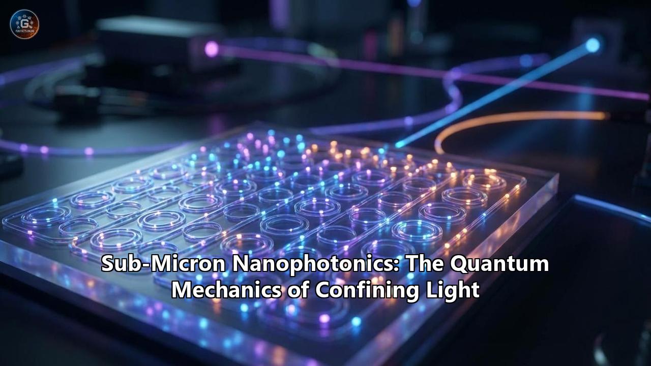
Welcome to the world of sub-micron nanophotonics: the art and science of trapping, manipulating, and squeezing light into impossibly small volumes. By forcing light to interact with matter on the nanoscale, researchers are not only bypassing the diffraction limit but also unlocking entirely new quantum phenomena. From altering the fundamental rates of chemical reactions to building the architecture for tomorrow's quantum computers, confining light has become one of the most exciting frontiers in modern physics.
Bypassing the Diffraction Limit: The Plasmonic Solution
To understand how we can squeeze light into a space smaller than its wavelength, we have to look at what happens when photons collide with a sea of electrons. The traditional approach to guiding light relies on dielectric materials, like the glass in fiber-optic cables, which bounce light back and forth using total internal reflection. However, dielectric waveguides are strictly bound by the diffraction limit.
Enter plasmonics. When light strikes the surface of a highly conductive metal (like gold or silver) under the right conditions, its energy couples with the free electrons on the metal's surface. This interaction creates a hybrid wave of light and undulating electrons known as a Surface Plasmon Polariton (SPP).
Because SPPs are tied to the mass and charge of the electrons, their effective wavelength is dramatically compressed compared to a free-flying photon. It is the optical equivalent of taking a wide, sweeping radio wave and compressing it into a tight, localized vibration. By engineering metallic nanostructures—such as tiny antennas, bowties, or spheres—scientists can create Localized Surface Plasmons (LSPs) that act as optical cavities. These structures can concentrate the electromagnetic field into volumes as small as a single cubic nanometer, concentrating light far beyond the diffraction limit.
Enter the Quantum Arena: Cavity Quantum Electrodynamics (cQED)
When light is compressed into these sub-micron plasmonic cavities, the rules of classical electromagnetism begin to break down, and Quantum Electrodynamics (QED) takes the wheel.
In classical physics, a vacuum is simply empty space. In quantum mechanics, however, a vacuum is a boiling sea of temporary electromagnetic fluctuations. When you shrink the volume of a cavity, you amplify the strength of these quantum vacuum fluctuations. This leads to a profound realization: the environment surrounding an atom or molecule dictates how that atom interacts with light.
This is best demonstrated by the Purcell Effect. If you take a quantum emitter—such as a fluorescent molecule or a semiconductor quantum dot—and place it in free space, it will absorb energy and eventually emit a photon at its own leisure. But if you place that exact same emitter inside a highly confined nanophotonic cavity, the enhanced vacuum fluctuations will "coax" the emitter into releasing its photon hundreds or even thousands of times faster. Nanophotonics allows us to engineer the quantum vacuum itself, controlling the exact moment and direction a photon is born.
The Strong Coupling Regime: When Light and Matter Merge
The interactions between light and matter inside a cavity are generally categorized into two regimes: weak coupling and strong coupling.
The Purcell effect occurs in the weak coupling regime. The cavity enhances the emission rate, but the photon and the molecule retain their distinct, separate identities. The photon is born and immediately escapes the cavity.
But what happens if the nanophotonic cavity is so perfectly tuned, and the light is so tightly confined, that the photon cannot immediately escape? This pushes the system into the strong coupling regime. Here, the quantum emitter releases a photon, but before the photon can leave, it is reabsorbed by the emitter. The energy bounces back and forth between the matter (the exciton) and the light (the plasmon or cavity photon) at an astonishing speed.
This rapid exchange of energy is described by the Jaynes-Cummings model. The oscillation is so fast that the system can no longer be described as a separate molecule and photon. Instead, they merge into a new, hybrid quantum quasiparticle called a polariton (or a plexciton, when specifically involving plasmons and excitons).
The creation of these hybrid states results in a phenomenon called Rabi splitting, where the original energy level of the system splits into two distinct energy states. This isn't just an abstract quirk of physics—it fundamentally changes the properties of the material.
Polariton Chemistry: Rewriting the Rules of Reactions
One of the most mind-bending applications of this strong coupling is the emerging field of polariton chemistry. Chemical reactions are dictated by the energy landscapes of molecules. Traditionally, chemists use heat, pressure, or catalysts to change how a reaction occurs.
Recently, however, researchers have discovered that simply placing chemical reactants inside a sub-micron optical cavity can alter their reaction rates—even in the dark, without any external lasers. The enhanced electromagnetic vacuum fields inside the cavity couple with the molecular vibrations of the chemicals, shifting their energy landscapes. This macroscopic QED effect means we can potentially use nanophotonic mirrors to catalyze chemical reactions, bypassing traditional thermodynamics.
Single-Photon Guns and Spasers
By mastering sub-micron light confinement, engineers are developing revolutionary new devices that operate purely on quantum principles.
Single-Photon Sources: The backbone of the future quantum internet relies on the ability to transmit data encoded in single, isolated photons. Creating a reliable "single-photon gun" is notoriously difficult. However, by coupling two-dimensional (2D) materials—like hexagonal boron nitride (hBN) or molybdenum disulfide (MoS2)—with nanophotonic cavities, researchers have successfully engineered room-temperature single-photon emitters. The cavity funnels the quantum emission perfectly into a waveguide, acting as a reliable, on-demand photon source for quantum cryptography. Nanolasers (Spasers): Traditional lasers cannot be miniaturized below half the wavelength of the light they emit. But by replacing the photons in a laser with surface plasmons, scientists have created the "spaser" (Surface Plasmon Amplification by Stimulated Emission of Radiation). Spasers generate coherent optical fields at the nanometer scale, offering a blueprint for ultra-fast, microscopic light sources that could one day replace the electronic transistors in our computer chips, allowing data to be processed at the speed of light without catastrophic heat generation.Metamaterials, Superlenses, and the Birth of Picophotonics
While plasmonics handles the confinement of light via metals, another branch of sub-micron nanophotonics achieves light manipulation through geometry. Photonic crystals and metamaterials are artificial structures engineered with repeating nano-patterns. These patterns are smaller than the wavelength of light, tricking the light into behaving as if it were passing through a material that doesn't exist in nature.
One of the most famous applications of this is the superlens. Natural materials always refract (bend) light in a positive direction. But by engineering the dispersion relations in photonic crystals, scientists can create materials with a negative refractive index. A metamaterial superlens can capture the rapidly decaying "near-field" light waves that usually never make it to our eyes, allowing us to image objects like single viruses or DNA strands well beyond the traditional diffraction limit.
As we push deeper into the 2020s, the field is evolving beyond nanophotonics into what researchers in 2026 are calling picophotonics. By utilizing "superoscillatory light"—where the local frequency of a specially engineered light wave oscillates faster than its highest Fourier component—physicists can localize and measure nanoscale objects with near-atomic precision. Topologically structured light, such as toroidal electromagnetic pulses and skyrmions, are now being used to create incredibly robust, non-diffracting beams that can carry ultra-high capacities of quantum information.
AI-Driven Design and the Commercial Frontier
Despite the magic of quantum nanophotonics, fabricating sub-micron structures that perfectly confine light is an engineering nightmare. The shapes required to achieve optimal strong coupling or perfect negative refraction are often highly unintuitive.
To solve this, the field has increasingly turned to Machine Learning and AI-assisted inverse design. Instead of a human physicist guessing that a microscopic gold ring might confine light well, an algorithm is given a target quantum optical response. The AI then works backward, generating highly complex, almost alien-looking nanostructures that perform light-bending tasks perfectly.
These computational leaps, combined with advanced large-area nanoimprinting and CMOS-compatible integration, are pulling nanophotonics out of the laboratory and into the global market. Projected to reach nearly $30 billion by 2032, the nanophotonics market is rapidly expanding. The demand is heavily driven by the need for high-speed optical interconnects in AI data centers, ultra-sensitive biosensors for healthcare, and highly efficient light-trapping mechanisms for next-generation solar cells and consumer OLED displays.
Conclusion
Sub-micron nanophotonics is much more than a masterclass in miniaturization. It is a fundamental rewriting of how humanity interacts with the electromagnetic spectrum. By squeezing light into the narrowest of corridors, we force it to reveal its quantum nature. We have transitioned from simply bouncing light off mirrors to engineering the quantum vacuum itself, bending the rules of chemistry, and generating hybrid states of matter and energy. As we continue to blur the line between the photon and the electron, the tiny, confined sparks of nanophotonics will undoubtedly illuminate the next great era of technology.
Reference:
- https://www.researchgate.net/publication/38075432_Nanophotonics_Lasers_go_beyond_diffraction_limit
- https://portal.findresearcher.sdu.dk/en/publications/towards-quantum-nanophotonics-from-quantum-informed-plasmonics-to/
- https://validate.perfdrive.com/?ssa=f6ea9ce6-d7aa-520b-2917-43a5207afe5a&ssb=02949284794&ssc=https%3A%2F%2Fopg.optica.org&ssi=cd093e5c-d3hy-0407-6885-1af05424acfe&ssk=botmanager_support@radware.com&ssm=20464428841615467130760909497888&ssn=daeb27f0a0d2c1b8da9e144f0b409ba37ceaca73b8a9-334f-fc21-80b47f&sso=cf1c121-87d0-188d74a6f4677f5d42824dde8e5c9ed69427c1ccda9cb385&ssp=43989699191774288889177429719599411&ssq=97469626670135223245166701231251180991502&ssr=MTgwLjE4OC4xNzQuMjg=&sst=python-requests%2F2.32.3&ssv=&ssw=
- https://pubs.acs.org/doi/10.1021/acs.jpclett.4c03439
- https://pmc.ncbi.nlm.nih.gov/articles/PMC11501129/
- https://www.mdpi.com/2072-666X/16/8/933
- https://www.youtube.com/watch?v=zqZ4ioh-pps
- https://www.nanophotonics.org.uk/niz/publications/
- https://www.azonano.com/article.aspx?ArticleID=6971
- https://substack.com/home/post/p-185051556