
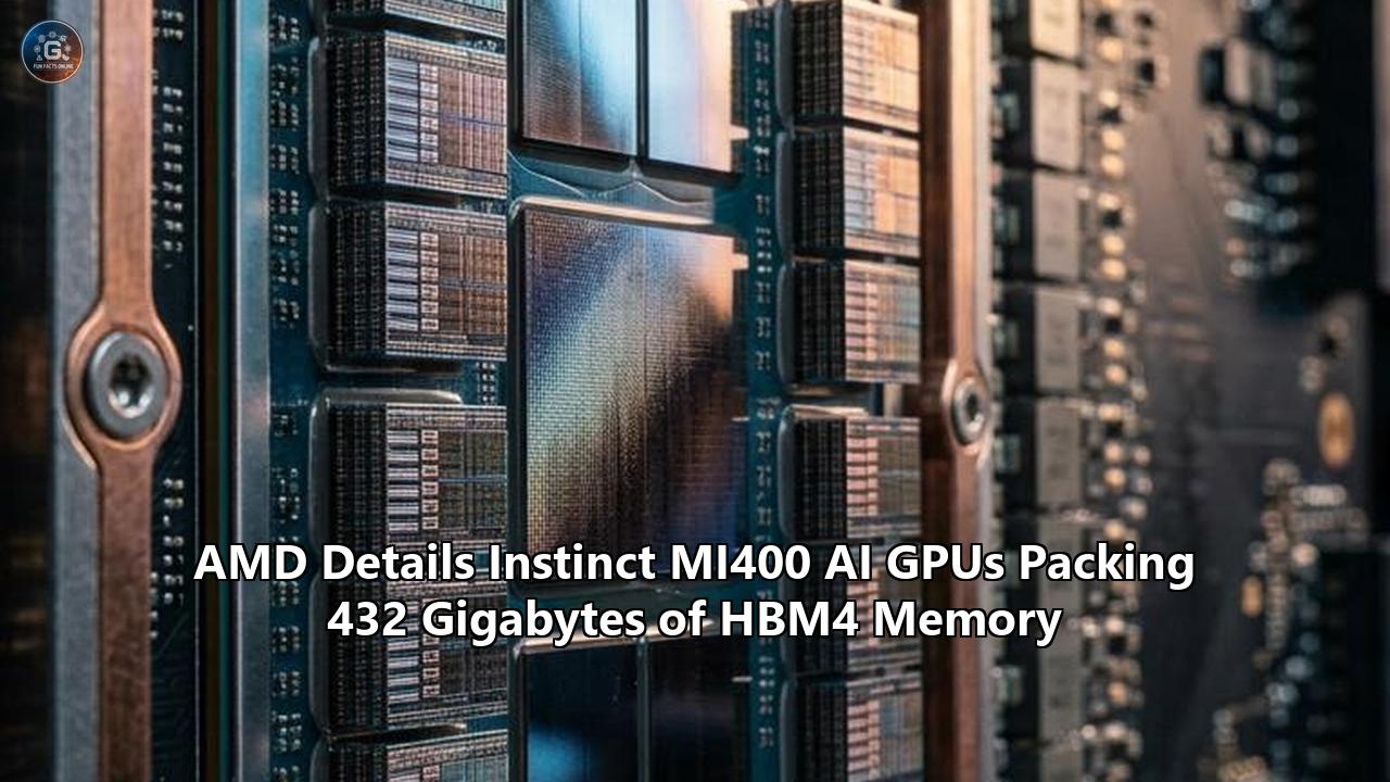
AMD has officially detailed the expanded architecture and deployment roadmap for its next-generation Instinct MI400 series graphics processing units, centering its offensive against Nvidia around an unprecedented memory configuration: up to 432 gigabytes of High Bandwidth Memory 4 (HBM4) per accelerator. The disclosure establishes the technical foundation for AMD’s CDNA 5 compute architecture and reveals three distinct processor tiers: the flagship MI455X built for hyperscale frontier artificial intelligence, the cost-and-capacity-optimized MI450X, and the scientific-focused MI430X.
Anchoring the reveal is a stark strategic divergence in data center architecture. While competing solutions from Nvidia’s Blackwell Ultra and upcoming Vera Rubin families allocate die area and power budgets toward specialized low-precision matrix multipliers and proprietary scale-up switching, AMD is wagering that the governing bottleneck of frontier machine learning has shifted permanently from raw compute throughput to memory capacity, on-package bandwidth, and open network interconnects.
“AMD Instinct MI400 Series GPUs bring leadership performance and new capabilities to AI and scientific computing,” said Andrew Dieckmann, corporate vice president and general manager of AMD’s Data Center GPU Business. “With advances in high-precision compute, new milestones in AI inference performance and an expanded range of configurations, we’re giving customers more options to power their next generation of AI and HPC workloads.”
In internal testing on its 72-GPU Helios rack-scale platform, AMD demonstrated that the MI455X achieved an inference throughput of 21,333 tokens per second per GPU on the DeepSeek-R1 model within an offline MLPerf Inference configuration. AMD reports this result outpaces published data for Nvidia’s Vera Rubin NVL72 by up to 30%, attributing the advantage to its memory subsystem delivering up to 23.3 terabytes per second (TB/s) of peak bandwidth and an open scale-up fabric providing 3.6 TB/s of bidirectional throughput per socket.
The announcement formalizes an escalating clash between two philosophies of data center infrastructure: a vertically integrated, proprietary ecosystem led by Nvidia, versus an open-consortium, memory-dominant paradigm assembled by AMD and its hyperscale allies.
Deconstructing the AMD Instinct MI400 Specs and CDNA 5 Architecture
A granular examination of the AMD Instinct MI400 specs reveals an aggressive reliance on modular 3.5D multi-die packaging, fabricated on TSMC’s leading-edge foundry processes. Rather than attempting to push monolithic reticle boundaries to their absolute physical limits, AMD has refined the chiplet methodology introduced in the MI300 and MI350 generations, isolating compute, memory, cache, and input/output functions across distinct process nodes.
+-----------------------------------------------------------------------------------+
|                           AMD INSTINCT MI455X OAM PACKAGE                         |
|                                                                                   |
|  +-------------+  +-------------+  +-------------+  +-------------+  +---------+  |
|  | HBM4 Stack  |  | HBM4 Stack  |  | HBM4 Stack  |  | HBM4 Stack  |  |  HBM4   |  |
|  | 36GB / 12-Hi|  | 36GB / 12-Hi|  | 36GB / 12-Hi|  | 36GB / 12-Hi|  |  Stack  |  |
|  +-------------+  +-------------+  +-------------+  +-------------+  +---------+  |
|  +-------------+  +=============================================+  +---------+  |
|  | HBM4 Stack  |  |        8x Accelerated Compute Dies (XCDs)   |  |  HBM4   |  |
|  | 36GB / 12-Hi|  |       Fabricated on TSMC N2P (2nm FinFET)   |  |  Stack  |  |
|  +-------------+  |         256 Work Group Processors (WGPs)    |  +---------+  |
|  +-------------+  |       Wave32 Execution / MXFP4 Math Engine  |  +---------+  |
|  | HBM4 Stack  |  +=============================================+  |  HBM4   |  |
|  | 36GB / 12-Hi|  |   2x Fabric & Cache Dies (FCD) (TSMC N3P)   |  |  Stack  |  |
|  +-------------+  |       192 MB Global Unified L2 Cache        |  +---------+  |
|  +-------------+  +=============================================+  +---------+  |
|  | HBM4 Stack  |  |      2x Enhanced I/O Dies (EAM) (TSMC N3P)   |  |  HBM4   |  |
|  | 36GB / 12-Hi|  |   36x UALoE Links (3.6 TB/s Scale-Up Bidir) |  |  Stack  |  |
|  +-------------+  +=============================================+  +---------+  |
|  +-------------+  +-------------+  +-------------+  +-------------+  +---------+  |
|  | HBM4 Stack  |  | HBM4 Stack  |  | HBM4 Stack  |  | HBM4 Stack  |  |  HBM4   |  |
|  | 36GB / 12-Hi|  | 36GB / 12-Hi|  | 36GB / 12-Hi|  | 36GB / 12-Hi|  |  Stack  |  |
|  +-------------+  +-------------+  +-------------+  +-------------+  +---------+  |
|                                                                                   |
|  Base Layer: TSMC CoWoS-L Advanced Packaging with 3D Hybrid Die-to-Die Bonding    |
+-----------------------------------------------------------------------------------+
The flagship MI455X accelerator integrates eight Accelerated Compute Dies (XCDs) manufactured on TSMC’s N2P (2-nanometer class) process node, stacked directly above active base interposer dies using true 3D hybrid bonding with copper-to-copper micro-bumps. The underlying base layer consists of two Fabric and Cache Dies (FCDs) and two dedicated Input/Output Dies (IODs), both built on TSMC’s N3P (3-nanometer class) node. This arrangement rests on a high-density TSMC Chip-on-Wafer-on-Substrate with Local Silicon Interconnect (CoWoS-L) substrate, yielding an integrated surface area that comfortably exceeds standard lithographic reticle windows.
At the execution core, CDNA 5 introduces a redesigned Work Group Processor (WGP) architecture. Moving away from the legacy Wave64 model that characterized earlier compute units, CDNA 5 defaults to a native Wave32 SIMD (Single Instruction, Multiple Data) execution mode. This design selection cuts execution latency and synchronization overhead in half when scheduling dynamic tensor kernels, significantly elevating operational arithmetic intensity.
Across its eight XCDs, the MI455X houses 256 active WGPs, incorporating advanced math engines with native support for Open Compute Project (OCP) Microscaling data formats (MXFP8, MXFP6, and MXFP4) equipped with block sizes of 16 and 32. This compute engine yields up to 40 petaflops (PFLOPS) of structured 4-bit floating-point (MXFP4) throughput and 20 PFLOPS of 8-bit floating-point (MXFP8) performance.
+--------------------------------------------------------------------------------------------------------------------------+
|                                    COMPREHENSIVE HARDWARE SPECIFICATION BENCHMARK                                        |
+------------------------------+--------------------+--------------------+--------------------+--------------------+-------+
| Metric / Feature             | AMD Instinct       | AMD Instinct       | AMD Instinct       | Nvidia Vera        | Nvidia|
|                              | MI455X             | MI450X             | MI430X             | Rubin              | B300  |
+------------------------------+--------------------+--------------------+--------------------+--------------------+-------+
| Architecture                 | CDNA 5             | CDNA 5             | CDNA 5             | Rubin              | Black.|
| Process Node (Compute)       | TSMC N2P (2nm)     | TSMC N2P (2nm)     | TSMC N2P (2nm)     | TSMC N3P (3nm)     | TSMC4N|
| Process Node (Base/IO)       | TSMC N3P (3nm)     | TSMC N3P (3nm)     | TSMC N3P (3nm)     | Monolithic/Multi   | CoWoS |
| Packaging Technology         | 3.5D CoWoS-L / 3D  | 3.5D CoWoS-L / 3D  | 3.5D CoWoS-L / 3D  | 2.5D CoWoS-L       | 2.5D  |
| HBM Memory Generation        | HBM4 (12-Hi)       | HBM4 (8-Hi)        | HBM4 (12-Hi)       | HBM4 (8-Hi/12-Hi)  | HBM3e |
| On-Package Memory Capacity   | 432 GB             | 288 GB             | 432 GB             | 288 GB             | 288 GB|
| HBM Stack Count              | 12 Stacks          | 8 Stacks           | 12 Stacks          | 8 Stacks           | 8 Stk |
| Peak Memory Bandwidth        | 23.3 TB/s          | 23.3 TB/s          | 23.3 TB/s          | 19.2 TB/s          | 8.0 TB|
| Interface Bus Width          | 24,576-bit         | 16,384-bit         | 24,576-bit         | 16,384-bit         | 8,192b|
| Global L2 Cache              | 192 MB             | 192 MB             | 192 MB             | ~128 MB            | 128 MB|
| Peak FP4 Tensor Throughput   | 40.0 PFLOPS        | 40.0 PFLOPS        | N/A (HPC focus)    | ~50.0 PFLOPS       | 13.5PF|
| Peak FP8 Tensor Throughput   | 20.0 PFLOPS        | 20.0 PFLOPS        | 10.0 PFLOPS        | ~25.0 PFLOPS       | 4.5 PF|
| Peak Native FP64 Vector/Mat  | Baseline Emulated  | Baseline Emulated  | 288 TFLOPS         | Minimal (~1.25 TF) | 1.25TF|
| Scale-Up Interconnect        | UALink / UALoE     | UALink / UALoE     | UALink / Infinity  | NVLink 6           | NVLink|
| Per-GPU Scale-Up Bandwidth   | 3.6 TB/s (Bidir)   | 3.6 TB/s (Bidir)   | 1.8 TB/s (Bidir)   | 3.0 TB/s (Bidir)   | 1.8 TB|
| Rack-Scale Solution          | Helios (72 GPUs)   | Helios (72 GPUs)   | Custom OEM / Exa.  | NVL72 (72 GPUs)    | NVL72 |
| Aggregate Rack Memory        | 31.1 TB HBM4       | 20.7 TB HBM4       | Workload Dependent | 20.7 TB HBM4       | 20.7TB|
| Aggregate Rack Bandwidth     | 1.67 PB/s          | 1.67 PB/s          | Workload Dependent | 1.40 PB/s          | 576TB |
| Target Power per Accelerator | ~1,200W - 1,400W   | ~1,000W - 1,100W   | ~1,000W            | ~1,200W            | 1,100W|
+------------------------------+--------------------+--------------------+--------------------+--------------------+-------+
The memory subsystem is where the hardware diverges most sharply from historical configurations. The JEDEC JESD238 HBM4 standard transitions from a 1,024-bit per-stack bus to a wide 2,048-bit interface. The MI455X integrates 12 distinct HBM4 stacks, producing an aggregate bus width of 24,576 bits routed across the CoWoS-L substrate. Using 12-high, 36-gigabyte (288-gigabit) dynamic random-access memory (DRAM) dies, the package hits its headline 432 GB capacity.
Operating across 192 individual physical memory channels, the subsystem achieves a peak theoretical memory bandwidth of 23.3 TB/s. This yields an effective pin signaling rate of approximately 7.6 to 7.8 gigabits per second (Gbps)—a measured physical frequency designed to operate well within stable signaling margins while outstripping narrower-bus implementations in raw data transfer.
The newly unveiled MI450X alters the capacity axis while maintaining compute parity. Built on the identical CDNA 5 core architecture and packing the full complement of 256 WGPs, the MI450X drops its stack count from 12 to eight 36 GB stacks, settling at 288 GB of total on-package capacity. By tuning the remaining eight HBM4 interfaces to run at higher burst frequencies, AMD preserves the full 23.3 TB/s of peak bandwidth. This configuration grants data center operators an accelerator that maintains identical mathematical and communicative properties while stripping out roughly one-third of the high-cost HBM silicon.
Memory Capacity Versus Compute Density: Competing Silicon Paradigms
Evaluating the AMD Instinct MI400 specs against competing architectures illustrates fundamentally divergent calculations regarding physical silicon allocation. In modern deep learning accelerators, total package area, power delivery envelopes, and thermal dissipation thresholds form an zero-sum equation. Silicon floor space assigned to memory interfaces and physical PHY blocks cannot simultaneously host mathematical tensor cores or massive scratchpad SRAM.
AMD Instinct MI455X Approach: Memory-First Allocation
+---------------------------------------------------------------------------------+
| [12x HBM4 Stacks: 432GB] <---> [24,576-bit Bus / 23.3 TB/s Bandwidth]          |
| [Extensive Silicon Area to PHYs/Routing]                                        |
| [Compute: 40 PFLOPS FP4] -> Maximizes model residency and un-sharded KV Caches  |
+---------------------------------------------------------------------------------+

Nvidia Vera Rubin NVL72 Approach: Compute-Density & Switching Allocation
+---------------------------------------------------------------------------------+
| [8x HBM4 Stacks: 288GB] <---> [16,384-bit Bus / 19.2 TB/s Bandwidth]           |
| [Maximum Silicon Area to Transformer Engines & Native NVLink 6 Transceivers]    |
| [Compute: ~50 PFLOPS FP4] -> Prioritizes peak dense compute & switched crossbars|
+---------------------------------------------------------------------------------+
Nvidia’s philosophy, evident across its Blackwell Ultra (B300) and upcoming Vera Rubin platforms, centers on maximizing mathematical compute density and preserving proprietary, single-cycle interconnect fabrics. The standard Rubin GPU design relies on eight HBM4 stacks, delivering 288 GB of memory—a direct match for the mid-tier AMD MI450X, but lagging behind the flagship MI455X’s 432 GB by 144 GB per socket.
Nvidia’s layout choices prioritize high-density FP4 Transformer Engines capable of approximately 50 PFLOPS of compute, along with dedicated silicon area for NVLink 6 high-speed transceivers and Tensor Memory Accelerators (TMA).
However, Nvidia’s pursuit of extreme per-pin signaling rates has encountered physical friction. Throughout early 2026, architectural projections for Vera Rubin cited memory bandwidth figures reaching 22 TB/s based on an aggressive pin transfer rate of 10.7 to 11.7 Gbps across its 2,048-bit per-stack interfaces. Subsequent revisions in official technical documentation adjusted these specifications downward to 19.2 TB/s per GPU, corresponding to an operational pin speed of roughly 9.3 to 9.4 Gbps. Simultaneously, bidirectional NVLink 6 scale-up bandwidth per GPU was modulated from 3.6 TB/s down to 3.0 TB/s, as signal integrity constraints at high Nyquist frequencies prompted adjustments in complex multi-rack chassis.
AMD bypassed these specific per-pin signaling hurdles by embracing horizontal scale on the package. Rather than driving fewer HBM4 channels at bleeding-edge clock rates, AMD incorporated 12 memory stacks across a 24,576-bit interface. Distributing electrical signaling across more physical pins allows the MI455X to hit 23.3 TB/s at conservative, power-efficient clock frequencies.
The tradeoff is complexity in packaging: routing 12 vertical HBM4 stacks alongside eight hybrid-bonded compute dies demands an expansive CoWoS-L interposer, multi-reticle stitch lines, and advanced substrate engineering that inherently challenge manufacturing yields.
The downstream economic consequences of these decisions are substantial:
- Silicon Cost and Bill of Materials (BOM): HBM4 is among the most expensive components in modern computing infrastructure. Incorporating 12 stacks on the MI455X drives package-level manufacturing costs well above an eight-stack design. AMD addresses this with the MI450X, matching Nvidia’s 288 GB capacity to compete on unit economics while preserving the MI455X as a premium configuration for workloads with strict memory footprints.
- Yield Tolerances: Twelve-stack CoWoS-L packaging introduces more points of failure during thermal compression bonding. A defect in a single DRAM stack or a broken micro-bump connection can compromise the entire package. AMD relies on Known Good Die (KGD) test protocols and active structural redundancy within its interposer to safeguard assembly yields.
- Power Allocation: Power delivery remains fixed at roughly 1,000 to 1,400 watts per board. Routing current to 12 HBM4 stacks consumes a larger slice of the thermal envelope, leaving less headroom for sustained high-frequency compute clocks. Nvidia preserves more of its thermal margin for raw matrix operations.
- Physical Footprint: Integrating 12 HBM stacks pushes the Open Accelerator Module (OAM) mechanical envelope to its dimensional limits, demanding custom baseboard modifications and tight cooling integration.
Inference Economics: The Shift to Memory-Bound Reasoning Models
The commercial contest between AMD and Nvidia is playing out across inference economics. Through 2024 and 2025, data center capital expenditures were heavily weighted toward foundational training runs, where dense matrix multiplication and continuous FP8/FP16 operations dominated.
By late 2026, spending has pivoted decisively toward operational inference, long-context retrieval, and agentic reasoning systems. Architectures such as DeepSeek-R1, OpenAI’s reasoning series, and Claude’s extended-thinking systems rely on reinforcement-learned chain-of-thought generation that outputs tens of thousands of intermediate tokens prior to returning an answer.
AUTOREGRESSIVE TOKEN GENERATION BOTTLENECK TRANSITION
+-----------------------------------------------------------------------------------+
| PREFILL PHASE: High Parallelism / Compute Bound                                   |
| Processing the entire input context simultaneously                                |
| Math Units Saturate (FLOPS Govern Speed)                                          |
+-----------------------------------------------------------------------------------+
                                         |
                                         v
+-----------------------------------------------------------------------------------+
| DECODE PHASE: Sequential Generation / Memory Bandwidth & Capacity Bound           |
| Fetching full model weights & historical KV Cache to generate ONE single token    |
| Operational Intensity Drops: Arithmetic Units Starve for Data                     |
| Speed = (Memory Bandwidth in TB/s) / (Bytes Moved per Token)                      |
+-----------------------------------------------------------------------------------+
Autoregressive transformer inference divides into two computational regimes: the prefill phase and the decode phase. In prefill, entire context windows are parsed concurrently, generating compute-dense matrix multiplications that saturate mathematical tensor units.
In decode, the engine generates output tokens one by one. For every single token generated across an active session, billions of model parameters must be read from high-bandwidth memory into the register files. Consequently, operational arithmetic intensity collapses. The execution speed of the decode phase is largely a direct function of memory bandwidth, while the number of concurrent sessions an accelerator can sustain without spilling data to system memory is dictated by its total on-package capacity.
This dynamic is amplified by the Key-Value (KV) cache. As context windows lengthen to accommodate multi-turn reasoning traces, memory consumption for historical attention states escalates. For a standard multi-head attention transformer, the memory required for the KV cache scales linearly with context length, layer count, attention heads, and active concurrent batch size:
$$\text{Memory}_{\text{KV}} = 2 \times b \times l \times h \times d \times n_{\text{bytes}}$$
Where $b$ is the concurrent batch size, $l$ is context length in tokens, $h$ is total hidden layers, $d$ is dimension per head, and $n_{\text{bytes}}$ represents numerical precision (e.g., 2 bytes for FP16, 1 byte for FP8).When an active reasoning model’s parameters and KV caches exceed the capacity of a single accelerator, the system must split the workload across multiple devices using Tensor Parallelism (TP), Pipeline Parallelism (PP), or Expert Parallelism (EP). Every split introduces communicative overhead: activations must cross physical inter-chip links, introducing latency penalties and consuming inter-GPU fabric bandwidth.
+--------------------------------------------------------------------------------------------------------------------------+
|                              MIXTURE-OF-EXPERTS (DEEPSEEK-R1 671B) DEPLOYMENT COMPARISON                                 |
+------------------------------------+---------------------------------------+---------------------------------------------+
| Operational Metric                 | AMD Instinct MI455X (432 GB HBM4)     | Competitor Baseline (288 GB HBM4/HBM3e)     |
+------------------------------------+---------------------------------------+---------------------------------------------+
| Minimum Sockets to Host Weights    | 2 GPUs (864 GB Total HBM)             | 3 to 4 GPUs (864 GB to 1,152 GB Total HBM)  |
| Sharding Strategy                  | Low-Degree Tensor / Expert Parallel   | High-Degree Sharding Required               |
| Network Hops per Decode Step       | 1 Intra-Domain Hop                    | Multiple Fabric Passes Across Trays         |
| Memory Remaining for KV Cache      | ~193 GB Free Space for Attention      | Constrained (~40 GB to 60 GB Remaining)     |
| Maximum Concurrent Sessions (128k) | Up to 4x Higher Concurrent Contexts   | Requires Context Paging or Offload          |
| Measured MLPerf Offline Throughput | 21,333 Tokens / Second / GPU          | Baseline (Normalized Index: 1.00)           |
| Throughput Advantage Delta         | Up to +30% vs. Published Vera Rubin   | Reference Performance Target                |
+------------------------------------+---------------------------------------+---------------------------------------------+
A practical example surfaces with DeepSeek-R1, an open-weights Mixture-of-Experts (MoE) model comprising 671 billion total parameters, of which roughly 37 billion activate per token. In an FP8 quantized format, the static weights alone demand approximately 671 gigabytes of resident memory.
On an accelerator equipped with 288 GB of HBM—such as the standard Vera Rubin or Blackwell Ultra B300—a minimum of three chips (yielding 864 GB raw capacity) is required simply to hold the base model, and four chips are required in real-world deployments to preserve sufficient headroom for operating caches and KV tables.
On the MI455X, two accelerators pool 864 GB of HBM4. Two devices comfortably absorb the static FP8 model weights with nearly 200 GB of pristine, high-speed memory left available for operational activations and extensive KV cache pools.
Halving the physical hardware boundary required to host an MoE model eliminates entire layers of communicative overhead. Instead of routing all-to-all expert routing tokens across eight or sixteen devices through a complex scale-up backplane, traffic remains consolidated across a dual-chip link. This architectural consolidation underpins AMD’s measured 21,333 tokens per second per GPU on DeepSeek-R1, illustrating how on-package memory headroom translates directly into sustained throughput gains.
Interconnect Frameworks: Open Standards Versus Proprietary Fabrics
Interconnect architectures govern the maximum size of a scale-up domain—the group of accelerators that can share memory and exchange tensor activations as if they were a single logical device. Here, the industry faces an explicit structural choice: Nvidia’s tightly coupled, proprietary NVLink-NVSwitch fabric, versus the multi-vendor, consortium-backed Ultra Accelerator Link (UALink) and Ultra Ethernet Consortium (UEC) standards.
PROPRIETARY VS. OPEN SCALE-UP AND SCALE-OUT NETWORKING STACKS

NVIDIA VERA RUBIN NVL72 PLATFORM (Proprietary Vertical Integration)
+---------------------------------------------------------------------------------+
| Compute: 72x Rubin GPUs + 36x Custom Olympus Vera CPUs                          |
| Scale-Up Fabric: NVLink 6 (3.0 TB/s Bidir per GPU / 216 TB/s Aggregate Rack)   |
| Switching Core: 9x Liquid-Cooled NVLink 6 Switch Trays (Custom ASIC Crossbars)  |
| Scale-Out Network: ConnectX-9 SuperNICs + Quantum-X800 InfiniBand / Spectrum-X  |
| Ecosystem: Single-Vendor Control (Nvidia Software, Silicon, Switches, Cables)   |
+---------------------------------------------------------------------------------+

AMD HELIOS RACKSCALE PLATFORM (Open Consortium Architecture)
+---------------------------------------------------------------------------------+
| Compute: 72x Instinct MI455X/MI450X GPUs + Zen 6 EPYC "Venice" Host Processors  |
| Scale-Up Fabric: UALink over Ethernet (UALoE) (3.6 TB/s Bidir / 260 TB/s Rack)  |
| Switching Core: Open Consortium Leaf-Spine / Direct-Mesh Switched Topology     |
| Scale-Out Network: AMD Pensando Pollara 400G/800G NICs + Ultra Ethernet (UEC)   |
| Ecosystem: Multi-Vendor Standardization (Open Accelerators, NICs, and Switches) |
+---------------------------------------------------------------------------------+
Nvidia’s approach across the GB200, GB300, and Vera Rubin NVL72 architectures relies on a closed hardware-software loop. In the Vera Rubin NVL72 rack, 72 Rubin GPUs interconnect across an internal passive copper backplane coordinated by nine centralized NVLink switch trays containing custom NVLink 6 ASICs. This design treats the 72 GPUs as a non-blocking crossbar domain where any GPU communicates with any other at full link speed.
Furthermore, Nvidia embeds NVLink In-Network Computing (SHARP) directly within its switch silicon, executing collective operations—such as MPI_Allreduce and vector arithmetic—inside the network substrate rather than on the GPUs themselves.
The structural advantage of this vertical approach is determinism. Network contention, packet drop, and routing jitter are strictly managed within the closed physical system.
The primary disadvantage is total architectural lock-in: an operator cannot decouple the GPU purchase from Nvidia’s switches, host CPUs, network interface cards, and management software. Upgrading the scale-up domain requires procuring the complete proprietary rack enclosure.
+--------------------------------------------------------------------------------------------------------------------------+
|                                    RACK-SCALE INTERCONNECT AND SYSTEM CAPABILITIES                                       |
+------------------------------------+---------------------------------------+---------------------------------------------+
| Architectural Property             | AMD Helios Solution (MI455X)          | Nvidia Vera Rubin NVL72 Platform            |
+------------------------------------+---------------------------------------+---------------------------------------------+
| Scale-Up Protocol                  | UALink 1.0 / UALoE                    | Sixth-Generation NVLink (NVLink 6)          |
| Open Consortium Backing            | UALink Consortium (AMD, Intel, Meta)  | Proprietary (Nvidia Exclusively)            |
| Per-GPU Bidirectional Scale-Up     | 3.6 TB/s (36 Links x 100 GB/s)        | 3.0 TB/s (Settled Specification Target)     |
| Aggregate Rack Scale-Up Bandwidth  | 260 TB/s                              | 216 TB/s                                    |
| Coherent Scale-Up Domain Size      | 72 GPUs (Standard Rack Enclosure)     | 72 GPUs (Single Coherent NVLink Domain)     |
| Scale-Out Network Protocol         | Ultra Ethernet Consortium (UEC Spec)  | Quantum-X800 InfiniBand / Spectrum-X        |
| Network Interface Engine           | AMD Pensando Pollara SuperNICs        | Nvidia ConnectX-9 SuperNICs / BlueField-4   |
| Aggregate Scale-Out Bandwidth      | 43 TB/s per Helios Cabinet            | Up to 32.4 TB/s to 38 TB/s per Rack         |
| Host Processor Platform            | AMD EPYC "Venice" (Zen 6 Microarch)   | Custom Nvidia Vera CPUs (Olympus Arm Cores) |
| Physical Rack Form Factor          | Open Double-Wide OCP Space Envelope   | 19-inch / 21-inch Modified OCP ORV3 Cabinet |
+------------------------------------+---------------------------------------+---------------------------------------------+
AMD has mounted its counter-offensive via the UALink Consortium, backed by a broad cohort including Broadcom, Cisco, Google, Hewlett Packard Enterprise, Intel, Meta, and Microsoft. The AMD Instinct MI400 specs implement UALink over Ethernet (UALoE) as the native intra-rack scale-up protocol.
Each MI455X GPU routes 36 bidirectional UALoE links via its two enhanced I/O dies, generating 3.6 TB/s of bidirectional scale-up bandwidth per socket. Within the 72-GPU Helios rack, this provides an aggregate scale-up fabric throughput of 260 TB/s—surpassing the 216 TB/s aggregate of the settled Vera Rubin NVL72 specification.
UALoE leverages standard high-speed Ethernet physical layer serialization/deserialization (SerDes) operating at 200 Gbps per lane, overlaying a low-latency, memory-semantic transaction layer that supports hardware-level direct memory access (RDMA) and memory coherency.
For scale-out networking beyond the rack, Helios utilizes Ultra Ethernet compliant AMD Pensando Pollara NICs, generating 43 TB/s of aggregate egress bandwidth without reliance on proprietary InfiniBand fabrics.
The tradeoffs between these networking strategies involve distinct operational variables:
- Software Tooling Maturity: NVLink’s collective communication library (NCCL) benefits from over a decade of production optimization across tens of thousands of supercomputing clusters. AMD’s collective communication primitives (RCCL) and early UALoE drivers must establish an equivalent record of stability and predictable load-balancing across multi-tier topologies without relying on specialized in-network hardware reduction engines.
- Topology and Cabling: Nvidia’s NVL72 relies on an internal passive copper cartridge spine to route thousands of high-speed differential pairs, circumventing optical transceivers at the expense of assembly weight and rigidity. Helios’s UALoE architecture permits disaggregated physical layouts, allowing standard active electrical cables (AEC) or optical links to bridge compute trays, broadening physical deployment options within standard data center footprints.
- Procurement Autonomy: Deploying Helios enables infrastructure architects to source switches and networking silicon from third parties such as Broadcom, Cisco, or Arista, preventing single-supplier price inelasticity. Conversely, integration testing for heterogeneous components shifts to the end-user or systems integrator.
High-Precision Scientific Computing: The MI430X Alternative
While commercial AI inference runs primarily on low-precision math formats like FP8 and FP4, traditional scientific computing, high-energy physics, computational fluid dynamics, and molecular modeling rely on native IEEE 754 double-precision 64-bit floating-point (FP64) calculations. Over the past three silicon generations, the broader GPU industry has gradually sidelined FP64 compute engines, dedicating hardware area almost exclusively to integer and low-precision floating-point matrix units.
+-----------------------------------------------------------------------------------+
|                    THE DIVERGENT PATH OF FP64 DOUBLE PRECISION                    |
|                                                                                   |
|  Nvidia Blackwell Ultra / Vera Rubin Track:                                       |
|  FP64 Demoted to Skeleton Baseline (~1.25 to 2.5 TFLOPS)                          |
|  Transistors reallocated entirely to FP4/FP8 Transformer Engines                  |
|  HPC codes forced into software emulation or legacy hardware                      |
|                                                                                   |
|  AMD Instinct MI430X Track:                                                       |
|  288 TFLOPS Native Hardware FP64 Compute Engine                                   |
|  432 GB HBM4 Memory Subsystem @ 23.3 TB/s                                         |
|  Targeted directly at Exascale Scientific Simulation & Sovereign Discovery Labs   |
+-----------------------------------------------------------------------------------+
Nvidia’s Blackwell Ultra B300 offers a stark illustration of this shift: its native hardware FP64 vector compute performance drops from the previous generation’s 37 TFLOPS down to approximately 1.25 TFLOPS, forcing HPC users to rely on emulated math libraries or remain on legacy Hopper hardware.
AMD has rejected this blanket deprioritization with the introduction of the Instinct MI430X. Built on the CDNA 5 foundation, the MI430X functions as a high-precision, memory-rich accelerator tailored specifically for national supercomputing facilities and sovereign scientific initiatives.
The MI430X delivers an unprecedented 288 TFLOPS of peak hardware-based native FP64 matrix performance. Crucially, AMD pairs this heavy arithmetic engine with the full 432 GB HBM4 memory subsystem and 23.3 TB/s of bandwidth found on the flagship MI455X.
Alongside the hardware reveal, AMD published an extensive research study examining 47 scientific workload configurations spanning 11 prominent benchmarks and applications, systematically evaluating the operational boundaries between software-emulated FP64 and hardware-native double precision. The findings indicate that while certain iterative solver algorithms tolerate reduced-precision preconditioning, fundamental scientific codes—including lattice quantum chromodynamics, seismic wave modeling, and relativistic hydrodynamic simulations—suffer severe numerical drift and convergence failures when stripped of native FP64 execution units.
The MI430X positions AMD as the primary supplier for next-generation sovereign infrastructure. Systems such as the upcoming Discovery supercomputer at Oak Ridge National Laboratory, along with Europe’s Alice Recoque and Herder exascale deployments, depend on hardware architectures capable of running converged workloads: coupling AI surrogate models (operating in FP8 or FP4) with multi-physics numerical solvers (demanding native FP64) without requiring separate, dedicated clusters.
Hyperscale Bifurcation: Custom Variants and Infrastructure Scale
The arrival of the MI400 family highlights an accelerating trend among hyperscale cloud providers: the bifurcation of computing fleets into general-purpose merchant infrastructure and tailored, workload-specific accelerator silicon.
AMD disclosed commercial commitments for its MI400 series that illustrate this divide. Major foundation model developers have reserved capacity, led by OpenAI’s multi-year 6-gigawatt infrastructure agreement and Anthropic’s planned deployment reaching up to 2 gigawatts. Oracle Cloud Infrastructure has separately booked over 50,000 MI455X units to anchor its bare-metal AI supercomputing instances. These frontier model creators require maximum memory capacity (432 GB) and peak bandwidth (23.3 TB/s) to train next-generation parameters and serve high-concurrency reasoning agents.
HYPERSCALE DEPLOYMENT PROFILES: FRONTIER AI VS. RECOMMENDATION SYSTEMS

OPENAI / ANTHROPIC / ORACLE (Frontier Reasoning & Multi-Modal Foundation Models)
+---------------------------------------------------------------------------------+
| Hardware Base: AMD Instinct MI455X (Full Specification OAM)                     |
| Memory Footprint: 432 GB HBM4 @ 23.3 TB/s (12 Stacks)                           |
| Mathematical Profile: Maximum FP4/FP8 Matrix Throughput (40 PFLOPS)             |
| Topology: 72-GPU Helios Liquid-Cooled Pods with UALoE Fabric Scale-Up           |
| Focus: Elimination of inter-node communication for multi-trillion parameter MoE |
+---------------------------------------------------------------------------------+

META PLATFORMS (Custom RecSys Engine Optimization)
+---------------------------------------------------------------------------------+
| Hardware Base: Tailored Custom AMD MI450 Variant                                |
| Memory Footprint: 144 GB HBM4 (6x 8-Hi Stacks)                                  |
| Mathematical Profile: Compute units cut by roughly 50%                          |
| Topology: Disaggregated CPU-to-GPU High-Bandwidth Serving Nodes                 |
| Focus: Maximizing cost efficiency and CPU-to-GPU memory ratios for ranking      |
+---------------------------------------------------------------------------------+
Conversely, Meta Platforms has charted a contrasting course, detailing an order for a custom, stripped-down variant of the MI450 accelerator tailored for its content ranking and recommendation systems (RecSys).
Recommendation engines across Facebook and Instagram present a distinct architectural challenge compared to large language models. They rely heavily on processing massive sparse embedding tables that require immense memory retrieval rates and high CPU-to-GPU bandwidth, but demand far less dense mathematical matrix multiplication.
Meta’s custom MI450 variant cuts the standard 432 GB memory down to just 144 GB across six 8-high HBM4 stacks, while reducing the active compute units by approximately half. This trade-off removes two-thirds of the expensive HBM4 stack inventory, cutting bill-of-materials costs while yielding an accelerator tailored to maximize embedding throughput per dollar.
This divergence underscores a maturing infrastructure market: the industry no longer assumes that a single flagship GPU architecture can serve every hyperscale workload at peak capital efficiency.
Software Ecosystem Realities: ROCm 7 Versus the CUDA Abstraction Layer
Historically, hardware specifications alone have proven insufficient to upend established data center dynamics. Nvidia’s long-standing competitive moat has rested on its Compute Unified Device Architecture (CUDA) software platform, which has enjoyed nearly two decades of software optimization, compiler maturity, and institutional developer mindshare.
DEVELOPMENT STACK ABSTRACTION: THE HARDWARE-AGNOSTIC PIVOT

+---------------------------------------------------------------------------------+
| High-Level Application Layer: PyTorch 2.x, JAX, Hugging Face Transformers       |
+---------------------------------------------------------------------------------+
                                         |
                                         v
+---------------------------------------------------------------------------------+
| Intermediate Compilation Layer: OpenAI Triton, TorchDynamo, vLLM, SGLang        |
+---------------------------------------------------------------------------------+
                         /                               \
                        v                                 v
+-----------------------------------------------+ +-------------------------------+
| AMD ROCm 7.x Software Platform                | | Nvidia CUDA 13 Ecosystem      |
| HIP Runtime / hipBLASLt / CK Kernels          | | CUDA Driver / cuBLAS / TensorRT|
| Native Wave32 Compilation                     | | PTX Assembly / TMA Optimization|
| RCCL Collective Comm Library                  | | NCCL Collective Comm Library  |
+-----------------------------------------------+ +-------------------------------+
                        |                                 |
                        v                                 v
+-----------------------------------------------+ +-------------------------------+
| AMD Instinct MI400 Silicon (CDNA 5)           | | Nvidia Vera Rubin (Rubin Arch)|
+-----------------------------------------------+ +-------------------------------+
AMD’s competitive viability for the MI400 generation relies on the simultaneous rollout of ROCm 7. In earlier deployments spanning the MI200 and early MI300 lifecycles, end-users frequently encountered compilation hurdles, brittle kernel translations, and incomplete library bindings within the Heterogeneous-Compute Interface for Portability (HIP) runtime.
Three industry-wide developments have altered this software landscape ahead of the MI400 ramp:
- Compiler Layer Decoupling: The machine learning software stack has largely decoupled from direct vendor-specific assembly code. High-level orchestration frameworks—predominantly PyTorch 2.x and JAX—now compile through intermediate representations such as OpenAI Triton and TorchDynamo. Modern AI kernels for operations like FlashAttention-3, dynamic quantization, and SwiGLU activations are routinely authored in Triton, which compiles down to either AMD CDNA or Nvidia CUDA machine code with equal programmatic standing.
- Dedicated Serving Engines: Inference deployments have coalesced around specialized, community-driven serving runtimes, notably vLLM and SGLang. Both systems maintain native, optimized backends for AMD’s Composable Kernel (CK) library, closing the performance gap in prefill-decode scheduling, PagedAttention management, and continuous batching.
- Wave32 Alignment: Earlier ROCm compilers struggled with mapping algorithms optimized for Nvidia’s 32-thread warps onto AMD’s native 64-thread wavefront hardware. CDNA 5’s transition to a native Wave32 execution mode removes this structural mismatch, eliminating runtime translation overhead and simplifying automated kernel generation.
Persistent friction points remain, however. Multi-node distributed debugging tools, profiling utilities, and fine-grained collective tuning for non-standard model architectures continue to lag behind Nvidia’s polished development suite. For frontier training clusters, extracting peak performance from AMD hardware still demands dedicated on-site engineering support.
Thermal Envelopes, Liquid Cooling, and Facility Scale
Deploying modern rack-scale artificial intelligence clusters requires complex facility retrofits. The aggregate electrical and cooling requirements of systems like AMD Helios and Nvidia Vera Rubin NVL72 challenge traditional data center infrastructure.
+-----------------------------------------------------------------------------------+
|                         FACILITY INFRASTRUCTURE WORKFLOW                          |
|                                                                                   |
|  Power Input: 415V AC 3-Phase Mains                                               |
|       |                                                                           |
|       v                                                                           |
|  Power Shelves: Integrated Rectification to 54V DC Busbars                        |
|       |                                                                           |
|       +---> Compute Trays: 72x Accelerators (130 kW - 150 kW Thermal Load)        |
|       |                                                                           |
|       +---> Interconnect Fabric: UALoE / NVLink Switch Infrastructure             |
|                                                                                   |
|  Cooling Architecture: Closed-Loop Direct-to-Chip Liquid Cooling (DLC-2)          |
|       |                                                                           |
|       v                                                                           |
|  Coolant Distribution Unit (CDU): Pumping Treated Facility Water                  |
|       |                                                                           |
|       +---> Inlet Water Temperature: Sustained up to 45°C (Warm-Water Support)    |
|       +---> Heat Dissipation: 92% to 98% Heat Capture Direct to Liquid Loop       |
+-----------------------------------------------------------------------------------+
Nvidia’s GB300 and Vera Rubin NVL72 racks concentrate 72 GPUs, accompanying Vera CPUs, and NVLink switch trays within a specialized, liquid-cooled cabinet. The entire rack enclosure generates a thermal load spanning 132 to 142 kilowatts (kW) under nominal operation, peaking near 155 kW. This equates to over 140 kilowatts concentrated onto a physical data center footprint of roughly 0.64 square meters—an operational profile far removed from traditional enterprise server racks that historically operated at 9 to 15 kW.
AMD’s Helios architecture adopts an Open Compute Project (OCP) compliant double-wide rack envelope. Housing 72 MI455X or MI450X accelerators, dual-socket host nodes powered by Zen 6 EPYC "Venice" CPUs, and Pensando Pollara networking trays, Helios operates across a similar 130 to 150 kW thermal band.
To manage this thermal density, both platforms mandate direct-to-chip liquid cooling (DLC-2) with liquid-cooled manifold backplanes, completely abandoning ambient air cooling for core processing silicon. Both system designs support facility water loop temperatures with inlet thresholds up to 45°C. Operating at warm-water inlet temperatures permits facilities to rely on evaporative cooling towers and dry coolers rather than energy-intensive mechanical chillers, maintaining target Power Usage Effectiveness (PUE) metrics below 1.15.
The structural difference centers on physical form factors: Nvidia relies on narrow, tightly coupled 600mm rack integration, while AMD’s Helios uses a broader double-wide layout designed to lower internal coolant pressure drops and simplify physical field serviceability for hyperscale data center technicians.
Architectural Trajectories and Industry Implications
AMD’s disclosure of the AMD Instinct MI400 specs marks a decisive shift in how accelerator performance is framed. For years, industry announcements focused almost exclusively on peak matrix floating-point operations. By prioritizing 432 GB of HBM4 memory, 23.3 TB/s of bandwidth, and an open 3.6 TB/s UALink scale-up interconnect, AMD is treating memory residency and inter-device communication as the primary arbiters of artificial intelligence infrastructure economics.
This memory-first strategy provides clear structural advantages for serving large, long-context reasoning models, but it operates alongside distinct architectural tradeoffs:
- Strengths: Unrivaled on-package memory capacity (432 GB) simplifies serving topologies for Mixture-of-Experts architectures like DeepSeek-R1, reducing communication hops and elevating tokens-per-second-per-dollar metrics. A native 288 TFLOPS FP64 compute tier on the MI430X secures a unique foothold in converged exascale scientific supercomputing. The UALink and Ultra Ethernet integration breaks single-vendor component lock-in.
- Vulnerabilities: Advanced 12-stack 3.5D packaging with 3D hybrid bonding presents substantial manufacturing yield challenges compared to simpler configurations. Peak dense FP4 matrix throughput trails Nvidia’s Vera Rubin by approximately 20%. Open-standard UALink and UEC software runtimes require ongoing field validation to match the plug-and-play stability of Nvidia’s mature NVLink and NCCL stack.
Over the coming quarters, attention will center on TSMC’s 2nm production ramp, dynamic yield rates for 12-high HBM4 memory stacks at Samsung and SK Hynix, and the deployment of production Helios clusters at anchor hyperscale customers.
As model context lengths stretch into the millions and enterprise deployments turn toward agentic reasoning engines, the data center contest will ultimately be decided on the memory bus: whether infrastructure is governed by how fast accelerators can execute mathematical matrix products, or how much working context they can keep resident in local silicon.
Reference:
- https://newsroom.amd.com/news/amd-advances-instinct-mi400-series-ai-scientific-computing/
- https://www.jaredwatkins.com/research/ai-accelerators/amd-instinct/mi400-helios/
- https://techbytes.app/posts/amd-instinct-mi400-hbm4-dominance/
- https://developer.nvidia.com/blog/inside-nvidia-rubin-gpu-architecture-powering-the-era-of-agentic-ai/
- https://axecompute.com/nvidia-blackwell-gpu-comparison/
- https://mirrorfrog.com/en/docs/cards/amd/mi450/
- https://iotdigitaltwinplm.com/amd-mi400-instinct-architecture-ai-training-2026/
- https://ecrionix.org/cxl/day-15-cxl-vs-alternatives-roadmap/
- https://www.vlsi.kr/en/nvidia-rubin-hbm4-pin-speed-9-3-en/
- https://www.vlsi.kr/en/amd-instinct-mi450x-mi400-hbm4-en/
- https://mlq.ai/news/meta-orders-custom-amd-mi450-accelerators-with-144gb-hbm4-one-third-standard-memory/
- https://www.nvidia.com/en-us/data-center/vera-rubin-nvl72/
- https://inferencex.semianalysis.com/chips/b300
- https://ictdistribution.net/blog/supermicro-nvidia-vera-rubin-nvl72-scaling-ai-performance-at-rack-level
- https://www.spheron.network/blog/nvidia-vera-rubin-nvl72-guide/
- https://www.techpowerup.com/354133/nvidia-cuts-hbm4-speed-and-nvlink-bandwidth-targets-for-vera-rubin
- https://note.com/loyal_myrtle1528/n/nc701c02b0c87?hl=en
- https://blog.sagamiyun.me/blog/scale-up-interconnect-war/
- https://www.engineering.com/amd-expands-instinct-mi400-series-with-new-gpu-options/
- https://www.spheron.network/blog/ualink-vs-nvlink-open-gpu-interconnect-2026/
- https://lenovopress.lenovo.com/datasheet/ds0215-lenovo-nvidia-vera-rubin-nvl72
- https://www.learnaiinfra.com/articles/ualink-vs-nvlink-can-the-industry-out-link-nvidia
- https://www.moduledge.com/blog/gb300-nvl72
- https://rcrtech.com/semiconductor-news/interconnects-nvlink-ualink-and-cxl/
- https://www.supermicro.com/datasheet/datasheet_Supermicro_NVIDIA_Vera_Rubin_NVL72.pdf