In the cathedral of modern computing, where silicon processors are the altars and data is the sacrament, a quiet crisis has emerged. For decades, the industry worshipped at the altar of Moore’s Law, relentlessly doubling transistor counts and clock speeds, assuming that if we could just think faster, we could solve the world’s problems. We built processors capable of executing trillions of operations per second. We designed neural networks with hundreds of billions of parameters. We constructed supercomputers that consume the power of small cities.
But we forgot one thing: a brain is useless if it cannot remember.
As we stand in 2026, the artificial intelligence revolution—the defining technological shift of our century—is not being throttled by a lack of computational power. It is being throttled by a lack of memory bandwidth. The GPU, once the undisputed king of the hill, now sits idle for microseconds at a time, starving for data that cannot be fed to it fast enough. The culprit—and the savior—is a technology known as High-Bandwidth Memory, or HBM.
This is the story of HBM: the most complex, expensive, and critical component in the modern computing stack. It is a story of physics, where engineers fight against heat and resistance at the atomic scale. It is a story of geopolitics, where nations vie for control over the supply chain of "AI gold." And it is the story of the "Memory Wall," the single greatest barrier standing between us and the next leap in artificial intelligence.
Part I: The Architecture of Speed
To understand why HBM is revolutionary, one must first understand the tyranny of the "Von Neumann bottleneck." Since the dawn of the digital age, computers have been architected with a separation between the processing unit (CPU or GPU) and the memory unit (DRAM). Data must travel back and forth between these two components through a bus—a digital highway.
For forty years, we relied on GDDR (Graphics Double Data Rate) memory. GDDR is planar; it sits on the motherboard next to the processor, connected by copper traces printed on the circuit board. It is reliable, cheap, and fast enough for video games. But as AI models grew from mere gigabytes to terabytes in size, GDDR hit a physical limit. To get more bandwidth, you needed wider buses (more wires), but you can only fit so many wires on a 2D motherboard before signal interference and power consumption become unmanageable.
Enter HBM.
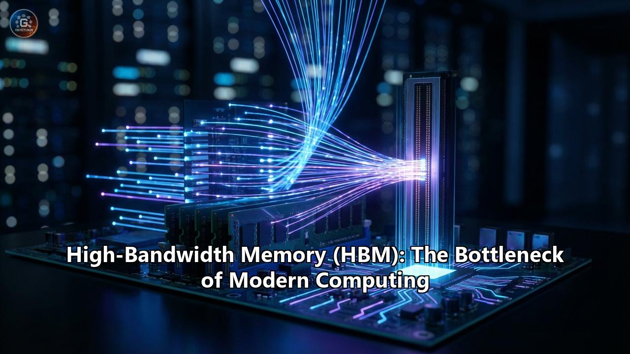
High-Bandwidth Memory is not just a better memory chip; it is a paradigm shift in 3D packaging. Instead of placing memory chips side-by-side on a motherboard, HBM stacks them vertically, like floors in a skyscraper.
1.1 The TSV: The Vertical Highway
The magic of HBM lies in the Through-Silicon Via (TSV). In a standard memory chip, data travels to the edge of the silicon die to exit through pins. In HBM, engineers drill thousands of microscopic holes through the silicon die itself. These holes are filled with conductive metal (usually copper), creating vertical elevators that allow data to shoot straight up and down the stack.
A single HBM stack can have thousands of these TSVs. This allows for an interface width that is orders of magnitude wider than traditional memory. While a standard GDDR6 chip might have a 32-bit wide interface, a single HBM stack operates on a 1024-bit wide interface (and with HBM4, this doubles to 2048-bit). It is the difference between a Ferrari on a two-lane road and a freight train on a thousand-lane highway. The Ferrari is faster (higher clock speed), but the freight train moves more cargo (higher bandwidth).
1.2 The Interposer: The Silicon Bridge
You cannot simply solder an HBM stack onto a standard plastic motherboard. The connections are too dense, numbering in the thousands within a few millimeters. To solve this, the industry invented the Silicon Interposer.
The interposer is a passive slice of silicon that sits between the GPU and the HBM stacks. It acts as an ultra-high-density bridge. Because it is made of silicon (like a chip) rather than fiberglass (like a motherboard), it can support wires that are nanometers thin. This 2.5D packaging allows the HBM to sit millimeters away from the GPU, reducing the distance data must travel, thereby slashing power consumption and latency.
Part II: The Evolution of HBM (2013–2026)
The history of HBM is a relentless march toward density and speed, driven entirely by the insatiable hunger of parallel computing.
HBM1 (2013): The Proof of Concept
The first generation, championed by AMD and SK Hynix, was a technological marvel but a commercial niche. It offered 128 GB/s of bandwidth per stack—impressive for the time, but limited to 4GB capacity. It proved the 3D stacking concept worked, but the manufacturing yield was low and the cost astronomical.
HBM2 & HBM2E (2016-2020): The Workhorses
HBM2 brought the technology to maturity. Bandwidth doubled to 256 GB/s per stack, and capacities grew to 8GB. This was the era where NVIDIA’s Tesla datacenter cards began to pull away from the competition. HBM2E later pushed speeds to 460 GB/s, becoming the standard for the early AI boom (GPT-2 era).
HBM3 (2022): The AI Explosion
HBM3 was the turning point. With bandwidths hitting 819 GB/s per stack, it enabled the NVIDIA H100 "Hopper" GPU to train massive Large Language Models (LLMs) like GPT-4. HBM3 allowed for 12-high stacks (12 dies stacked on top of each other), pushing capacity to 24GB per chip. A single H100 with six HBM3 stacks offered 80GB of ultra-fast memory.
HBM3E (2024-2025): The Current Standard
As of late 2025, HBM3E is the dominant force. It is an optimization of HBM3, pushing speeds to 1.2 TB/s per stack. SK Hynix and Micron led this charge, utilizing 1b-nanometer DRAM nodes. The "E" stands for Extended, but it effectively meant "Essential" for the Blackwell generation of GPUs. HBM3E enabled 12-high and 16-high stacks, delivering up to 36GB and 48GB per package.
HBM4 (2026): The Logic Integration Era
Now, we arrive at HBM4. This is the biggest architectural shift since the inception of HBM.
- 2048-bit Interface: The interface width doubles. To keep power in check, clock speeds are moderated, but the massive lane count ensures bandwidths exceed 2 TB/s per stack.
- Logic Base Die: Previous HBM generations used a simple buffer die at the bottom of the stack. HBM4 allows this base die to be a logic process (like 12nm or 5nm FinFET). This means the memory controller can move inside the memory package, or even perform basic computation (Processing-In-Memory or PIM) right at the source of the data.
- Direct Bonding: The vertical height constraints are so severe that traditional microbumps (solder balls between layers) are becoming a liability. HBM4 pushes the industry toward hybrid bonding—fusing copper directly to copper without solder—though this transition is fraught with yield challenges.
Part III: The Manufacturing Nightmare
Why is HBM the bottleneck? Why can't we just make more of it? The answer lies in the extreme difficulty of its manufacturing process. Making HBM is less like manufacturing a car and more like building a watch while wearing boxing gloves.
3.1 The Yield Trap
A standard DRAM wafer might yield 90% good chips. But HBM requires stacking 8, 12, or 16 of these chips. If one chip in the stack is defective, the entire stack is trash.
Mathematically, if a single die has a 98% yield, a 16-high stack has a yield of $0.98^{16} \approx 72\%$. In reality, the mechanical stress of stacking lowers this further. This is known as "compounded yield loss," and it makes HBM exorbitant to produce.
3.2 The Thermal Battle: MR-MUF vs. TC-NCF
The two Korean giants, SK Hynix and Samsung, took different paths to solve the heat and stability problem.
- TC-NCF (Thermal Compression with Non-Conductive Film): Samsung and Micron traditionally used this. They place a non-conductive film between layers and use heat and pressure to melt the solder bumps. It is robust but can be slow and prone to bending (warpage) as the stack gets higher.
- MR-MUF (Mass Reflow with Molded Underfill): SK Hynix bet on this technology. They attach the chips and then flood the gaps with a liquid epoxy molding compound (EMC). This liquid fills the voids and cures into a hard, heat-dissipating stone. MR-MUF proved superior for heat dissipation and production throughput in the HBM3 era, giving SK Hynix a massive lead in yields and market share (over 60% in 2025).
As we move to 16-high stacks in HBM4, the gaps between chips are becoming so small that even liquid epoxy struggles to flow. This is forcing a convergence toward Hybrid Bonding, where there are no bumps at all—just perfectly polished copper surfaces held together by Van der Waals forces and heat.
Part IV: The Market Landscape (2026)
The HBM market is not a free market; it is an oligopoly defined by technical capability.
1. SK Hynix: The King of the HillSK Hynix bet the farm on HBM when others hesitated, and it paid off. By perfecting MR-MUF, they became the primary supplier for NVIDIA. In 2026, they still command over 55% of the market. Their HBM3E is the gold standard, and their HBM4 yields are reportedly the highest in the industry.
2. Samsung Electronics: The Sleeping Giant WakesSamsung, the world’s largest memory maker, was famously late to the HBM3 party, suffering from yield issues with their TC-NCF process. However, 2026 is their comeback year. By adopting a hybrid approach and leveraging their turnkey service (offering Memory + Foundry + 2.5D Packaging all in-house), they are clawing back market share, aiming for 30%. Their "Shinebolt" HBM3E and subsequent HBM4 designs are now qualified in major hyperscaler chips.
3. Micron Technology: The American ContenderMicron, the sole US-based player, holds about 20% of the market. They skipped HBM3 to jump straight to HBM3E, a risky move that succeeded. Their 1-beta manufacturing node is highly efficient, and their HBM3E consumes roughly 30% less power than competitors, making them a favorite for power-constrained data centers.
Part V: The Bottleneck Explained
The term "bottleneck" is used loosely in tech, but for HBM, it is literal.
1. Capacity vs. Compute RatioAI models are growing faster than memory density. A GPT-4 class model requires terabytes of VRAM to run purely in memory. A single GPU cluster might have petaflops of compute but only terabytes of memory. The GPUs spend vast amounts of energy simply waiting for data to be fetched from the HBM.
2. The Supply Chain ChokeThere is a limited global supply of the specialized equipment needed to make HBM. The Thermo-Compression Bonders and TSV Etchers are backordered for 18 months. You cannot simply "spin up" an HBM line; it takes two years to build and qualify a facility. This inelastic supply curve means that even as demand from OpenAI, Google, and Meta triples, supply only creeps up linearly.
3. The Thermal WallHBM stacks run hot. They are placed millimeters from a GPU that runs at 80°C. Memory cells leak data when they get hot; if they get too hot (above 95°C), they lose data entirely. To prevent this, the refresh rate of the memory must be increased, which consumes more power and generates more heat. It is a vicious thermal cycle. The industry is currently designing liquid cooling that touches the silicon directly to solve this.
Part VI: The Future - HBM4 and Beyond
As we look toward the latter half of 2026 and into 2027, the roadmap is clear but treacherous.
Custom HBM (The "Foundry-fication" of Memory)With HBM4 allowing a logic base die, customers like NVIDIA and Google are asking to design that base die themselves. They want to put their own proprietary logic into the memory stack. This changes the business model of memory from "selling commodities" to "foundry services." HBM is becoming a custom ASIC.
Optical Interconnects (Silicon Photonics)Eventually, copper wires will fail us. The resistance is too high at HBM speeds. The holy grail is to replace the electrical traces on the interposer with light. Companies are experimenting with co-packaged optics (CPO) where the HBM communicates with the GPU via photons, virtually eliminating heat and latency over distance.
The End of the Road?Is there an HBM5? Yes, but it may look very different. We are approaching the height limit of physical stacking before the stack becomes mechanically unstable. Future memory might move to "3.5D" structures or utilize capacitor-less DRAM (like 3D X-Point derivatives) to increase density without height.
Conclusion
High-Bandwidth Memory is the unsung hero of the AI age. It is the most sophisticated component in your AI accelerator, a marvel of vertical integration and atomic precision. It is also the most fragile link in the chain. The shortage of HBM is the primary reason why AI accelerators cost $30,000 instead of $3,000.
As we navigate 2026, the resolution of the HBM bottleneck will determine the pace of AI progress. If the engineers at SK Hynix, Samsung, and Micron succeed in yielding HBM4 at scale, we will unlock the next generation of intelligence. If they fail, the AI revolution will not stall, but it will face a long, hot, and expensive summer.
In the end, the bottleneck is not just silicon; it is the fundamental physics of moving information through space. And in this battle against physics, HBM is our sharpest weapon.
Reference:
- https://files.futurememorystorage.com/proceedings/2025/20250807_DRAM-301-1_Tom-Hsu.pdf
- https://www.tekedia.com/memory-crunch-how-ais-relentless-appetite-is-rewriting-the-economics-of-computing/
- https://www.reddit.com/r/BlackboxAI_/comments/1pjg1du/why_the_real_bottleneck_of_the_ai_era_is_shifting/
- https://medium.com/@ben_pouladian/nvidias-secret-weapon-dominating-the-hbm-memory-bottleneck-ee284b53b298
- https://www.youtube.com/watch?v=j8TFFhQ2s40
- https://ponderwall.com/index.php/2025/12/14/high-bandwidth-memory-ai-bottleneck/
- https://en.wikipedia.org/wiki/High_Bandwidth_Memory
- https://www.rambus.com/blogs/hbm3-everything-you-need-to-know/
- https://community.cadence.com/cadence_blogs_8/b/fv/posts/high-bandwidth-memory-evolution-from-first-generation-hbm-to-the-latest-hbm4
- https://businessengineer.ai/p/the-ai-memory-chokepoint
- https://www.notebookcheck.net/Samsung-s-HBM4-memory-enters-trial-production-with-mass-production-targeted-for-late-2025.941385.0.html
- https://news.skhynix.com/2026-market-outlook-focus-on-the-hbm-led-memory-supercycle/
- https://www.supermicro.com/en/glossary/hbm4
- https://www.semiconsam.com/p/2026-hbm-a-shift-from-monopoly-to
- https://www.tomshardware.com/tech-industry/hbm4-mass-production-delayed-as-nvidia-pushes-memory-specs-higher
- https://zonglen.com/en/4/2/1782764