The era of artificial intelligence is fundamentally an era of computational hunger. As the global economy pivots toward AI-driven automation, scientific discovery, and real-time generative models, the underlying hardware powering these systems is hitting a physical and architectural wall. We have scaled our models to trillions of parameters, yet we find ourselves trapped by the speed at which we can move data.
In the high-stakes race toward Artificial General Intelligence (AGI), the dominant bottleneck is no longer simply raw compute capability—it is latency. The microsecond delays incurred when shuffling data between memory and processors, multiplied across massive clusters of discrete chips, accumulate into a massive barrier known as the "Memory Wall".
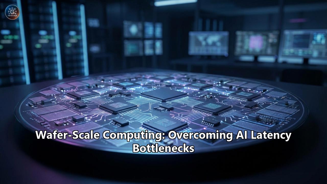
Enter Wafer-Scale Computing.
By fundamentally reimagining semiconductor manufacturing—abandoning the decades-old practice of slicing silicon wafers into tiny, discrete chips in favor of treating the entire dinner-plate-sized wafer as a single, monstrous processor—engineers have forged a path around the physical limits of traditional hardware. This architectural leap offers unimaginable memory bandwidth, zero off-chip communication penalties, and inference speeds that make traditional Graphics Processing Units (GPUs) look antiquated.
This comprehensive exploration delves into the mechanics of the AI latency bottleneck, the revolutionary engineering behind wafer-scale architectures like the Cerebras Wafer-Scale Engine (WSE), and how this paradigm shift is single-handedly rewriting the rules of AI training, real-time inference, and high-performance computing.
The Invisible Wall: Understanding AI's Latency Crisis
To understand the solution, we must first dissect the problem. For over a decade, the GPU has been the undisputed workhorse of the AI revolution. Originally designed to render polygons for video games, GPUs rely on massive parallel processing, making them fortuitously well-suited for the matrix multiplications required by deep learning. However, GPUs were never explicitly built for AI; they were adapted for it.
As models have grown exponentially—scaling 25,000 times faster than Moore’s Law at its peak—the fundamental architecture of the GPU has begun to show its strain.
The Anatomy of the Memory Wall
Modern AI workloads, particularly Large Language Models (LLMs) like those powering generative AI, are not compute-bound; they are memory-bandwidth-bound. When an LLM generates a response, it undergoes a process called inference. During text generation, the model predicts the next token (a chunk of a word) based on the preceding context. This operation relies heavily on General Matrix-Vector Multiplication (GEMV).
In a GEMV operation, the entire weight of the neural network (which can be hundreds of gigabytes in size for a frontier model) must be streamed through the compute cores to generate a single token. Because traditional GPUs have limited on-chip memory (typically around 50 to 100 megabytes of ultra-fast SRAM), the vast majority of the model's parameters must be stored in external High Bandwidth Memory (HBM).
The processor is remarkably fast, but it is constantly starved for data. It must wait for the parameters to travel from the HBM, across the chip's physical interfaces, and into the compute cores. This journey, though measured in nanoseconds, is an eternity in the realm of computing. The compute cores sit idle, burning power while waiting for data to arrive—a phenomenon known as the "Memory Wall".
The Cluster Catastrophe
To mitigate the fact that a single GPU cannot hold a massive LLM, engineers cluster thousands of GPUs together. Models are partitioned using complex software techniques like pipeline parallelism and tensor parallelism. However, this introduces an even more severe latency penalty: interconnect overhead.
When GPU A needs to send data to GPU B, the data must leave the processor, travel through the HBM, traverse a high-speed external interconnect (like Nvidia's NVLink or PCIe), pass through network switches (like InfiniBand or Ethernet), and finally arrive at the destination. No matter how fast these interconnects become, they are subject to the laws of physics. Moving electrons over copper cables or even photons over fiber optic links across a massive data center introduces unavoidable latency.
In a distributed cluster, the system is only as fast as its slowest link. Amdahl's Law dictates that the communication overhead eventually cancels out the benefits of adding more processors. The result? Skyrocketing power consumption, diminishing returns on performance, and an agonizingly complex software stack required just to keep the cluster synchronized.
The Paradigm Shift: What is Wafer-Scale Computing?
If the problem is the distance data must travel between memory and compute, and between discrete chips in a cluster, the logical solution is to eliminate the distance.
In traditional semiconductor manufacturing, a large silicon wafer (typically 300mm or 12 inches in diameter) is etched with hundreds of identical chip designs. The wafer is then cut (diced) into individual chips, which are packaged separately. This is done because defects are inevitable in silicon fabrication. A microscopic dust particle can ruin a transistor. By cutting the wafer into small chips, manufacturers can simply throw away the defective ones and keep the working ones, ensuring a profitable yield.
Wafer-Scale Computing throws this conventional wisdom out the window. Instead of cutting the wafer into hundreds of small chips, the entire wafer is kept intact and wired together to act as one colossal, unified processor.
The most prominent pioneer of this technology is Cerebras Systems. Their flagship processor, the Wafer-Scale Engine (WSE), represents a masterclass in extreme engineering and serves as the definitive counter-architecture to traditional GPU clusters.
Inside the Behemoth: The Cerebras WSE-3
To grasp the magnitude of wafer-scale computing, one must look at the specifications of the Cerebras WSE-3, the third generation of this revolutionary architecture launched to tackle the most demanding AI workloads.
Manufactured on a TSMC 5-nanometer process, the WSE-3 is a physical monolith:
- Size: 46,225 square millimeters. It is roughly the size of a dinner plate, making it 56 times larger than the largest GPU.
- Transistors: 4 trillion. To put this in perspective, Nvidia’s cutting-edge B200 GPU houses 208 billion transistors. The WSE-3 has nearly 20 times more.
- Compute Cores: 900,000 AI-optimized cores. These cores are entirely unburdened by legacy graphics hardware; they are pure AI calculating engines built for sparse tensor operations.
- On-Chip Memory: 44 Gigabytes of ultra-fast static RAM (SRAM). This is the critical differentiator. While GPUs rely on external HBM, the WSE-3 holds 44 GB of memory directly on the silicon, just one clock cycle away from the compute cores.
- Memory Bandwidth: 21 Petabytes per second. This is not a typo. 21 Petabytes—or 21,000 Terabytes—per second. This represents a 7,000-fold increase in memory bandwidth compared to traditional GPUs, completely shattering the memory wall.
- Peak Compute: 125 Petaflops of AI performance on a single piece of silicon.
Because the WSE-3 keeps 44GB of high-speed memory on-chip, it can store the entirety of massive LLMs (or large contiguous blocks of trillion-parameter models) directly next to the cores. There is no off-chip HBM to wait for. There are no PCIe lanes to bottleneck the data. There are no copper NVLink cables adding latency. Everything occurs within a unified silicon domain, allowing data to move at the speed of thought.
Engineering the Impossible: Defect Tolerance, Power, and Cooling
For decades, the semiconductor industry viewed wafer-scale integration as a "pipe dream". In the 1980s, companies like Trilogy Systems attempted to build wafer-scale chips but failed catastrophically due to manufacturing yields and thermal issues. So, how did modern engineers overcome the laws of physics that doomed previous attempts?
1. Solving the Yield Problem via Defect Tolerance
The primary argument against wafer-scale chips has always been yield. Statistically, a 12-inch silicon wafer will have microscopic flaws. If the entire wafer is one chip, a single defect should theoretically ruin the entire multi-million-dollar piece of silicon.
The solution lies in redundancy and highly advanced routing architecture. The WSE is not one giant monolithic core; it is a mesh of 900,000 independent compute cores connected by a high-speed "Swarm" fabric. During manufacturing, engineers intentionally build more than 900,000 cores on the wafer. Once the wafer is fabricated, it undergoes rigorous testing to identify which cores contain physical defects.
The system then utilizes internal routing logic to map around the dead cores. If Core A needs to connect to Core B, but the silicon between them is flawed, the fabric seamlessly routes the data through an adjacent, functioning path. This software-defined, hardware-enforced defect tolerance ensures that even with a normal distribution of manufacturing flaws, the wafer functions perfectly as a unified whole, maintaining a 100% yield for the usable product.
2. Advanced Packaging and Scribe Line Routing
Traditionally, wafers have "scribe lines"—empty spaces between chip dies where the mechanical saw cuts the wafer. To make a wafer-scale chip, engineers had to figure out how to transmit data across these scribe lines so the individual dies on the wafer could talk to each other.
Cerebras developed proprietary interconnect technology that spans these scribe lines, stitching the individual dies into a single, cohesive communications network. This die-to-die connection offers up to 10 times more bandwidth per unit area and a 100 to 300 times latency benefit compared to conventional PCB-based chip-to-chip interconnections like PCIe or NVLink.
3. Taming the Heat and Delivering Power
A silicon chip the size of a dinner plate containing 4 trillion transistors consumes a massive amount of electricity. The WSE-3 system operates at roughly 23 kilowatts of power. Delivering 23 kW of power uniformly across the surface of a silicon wafer, and then extracting the resulting heat without cracking the fragile silicon, is a monumental thermodynamic challenge.
Traditional edge-power delivery (sending electricity from the edges of the chip) is impossible at this scale; the current would drop off before reaching the center. Instead, power is delivered perpendicularly across the entire face of the wafer.
To cool the system, the wafer is packaged in a highly specialized system (the CS-3 Node) that utilizes complex liquid cooling. A specialized cold plate circulates fluid directly above the silicon, drawing heat away uniformly. While this requires sophisticated water-cooling infrastructure, it replaces the need for dozens of air-cooled racks in a traditional GPU cluster, dramatically reducing the overall data center footprint and total cost of ownership (TCO).
Inference at the Speed of Thought: The Real-Time AI Revolution
The true validation of wafer-scale computing is not found on a spec sheet; it is found in the physical reality of AI inference. In the era of interactive AI, milliseconds matter.
A user waiting for a chatbot to generate a response, or an autonomous agent waiting for a multi-step logic chain to resolve, is highly sensitive to latency. Traditional GPU clusters process LLMs at a rate of 20 to 50 tokens per second for a single user. This is slightly faster than human reading speed, which is acceptable for simple chatbots. However, as the AI industry evolves, this speed is no longer sufficient.
The Demands of Agentic and Reasoning AI
We have entered the era of "Reasoning Models". Models like OpenAI's o1 and o3, DeepSeek-R1, and Alibaba's Qwen3-32B do not simply spit out an immediate answer. They employ "Chain of Thought" reasoning. Before showing the user a final answer, they generate hundreds or thousands of hidden "thinking" tokens, exploring multiple logic pathways, fact-checking themselves, and executing planning algorithms.
If a model needs to generate 5,000 hidden tokens before providing an answer, a GPU running at 50 tokens per second will force the user to wait nearly two minutes. This latency breaks the utility of AI in fast-paced enterprise environments, high-frequency trading, and real-time robotics.
Shattering the Speed Limit
Because the WSE-3 stores the model weights directly in its 44GB of on-chip SRAM, and accesses them at 21 Petabytes per second, it eradicates the memory bottleneck associated with GEMV operations.
The results are staggering. On an open-weights 70-billion-parameter model (like Meta's Llama 3), a Cerebras wafer-scale system can generate a verified 2,100 tokens per second. This is roughly 70 times faster than a traditional GPU cluster. For smaller models or specialized architectures, the speed can exceed 2,000 tokens per second, essentially delivering instant, real-time reasoning.
When reasoning models like Qwen3-32B run on wafer-scale architecture, they can perform sophisticated, multi-step logic and output a response in as little as 1.2 seconds—drastically outperforming the speed of top-tier models running on conventional hardware. This unlocks entirely new frontiers for AI:
- Instantaneous Search: AI search engines like Perplexity can synthesize dozens of web pages and generate a heavily cited response in the blink of an eye.
- Autonomous Software Engineering: AI coding agents (like those developed by NinjaTech and Cognition) can test, compile, debug, and rewrite code loops continuously without being stalled by inference latency.
- Real-time Voice Interfaces: AI voice agents can finally converse without the awkward 2-second pause that breaks the illusion of natural human interaction.
Streamlining the Scale: The Death of Distributed Complexity
Latency is not just a hardware problem; it creates a software nightmare. When training massive AI models—some nearing or exceeding a trillion parameters—the models vastly exceed the memory capacity of even a wafer-scale chip. They must be trained across clusters of machines.
In a traditional GPU cluster, distributing a massive neural network is an exercise in agonizing complexity. Because GPUs are connected by relatively slow network links, developers must carefully slice the neural network apart. They use Tensor Parallelism to split layers across GPUs, Pipeline Parallelism to split different layers across different servers, and Data Parallelism to copy the model to process different data batches. The network traffic must be meticulously choreographed; if one GPU stalls, the entire cluster sits idle, wasting hundreds of thousands of dollars in compute time.
Weight Streaming: Single-Device Simplicity
Wafer-scale systems solve this through an architecture known as "Weight Streaming". Because the WSE is so massive and fast, it fundamentally changes the execution model.
Instead of slicing the neural network into tiny pieces and scattering them across thousands of chips, the wafer-scale system keeps all of its massive compute cores focused on the data. The model weights are stored in central, massively scalable external memory appliances (capable of supporting up to 1.2 Petabytes of memory). The weights are then streamed onto the wafer, layer by layer, in a continuous flow.
The entire wafer processes one layer of the neural network at a time, instantly, before moving to the next. From a software perspective, a cluster of wafer-scale chips (like the CS-3 AI supercomputer, which can be clustered up to 2,048 nodes) looks and behaves exactly like a single, gigantic processor.
This single-device simplicity means that researchers no longer need to write complex parallelization code. An AI scientist can define a 24-trillion parameter model with the same few lines of code used for a small model on a laptop. The infrastructure handles the scale automatically, dramatically accelerating the pace of AI research and lowering the barrier to entry for training frontier foundation models.
Beyond Generative AI: Scientific Supercomputing
While LLMs dominate the headlines, wafer-scale computing is proving equally transformative in High-Performance Computing (HPC) and scientific research.
The physical universe is governed by localized interactions. Whether simulating the airflow over an airplane wing (Computational Fluid Dynamics), the folding of a protein (Molecular Dynamics), or the spread of heat through a material, scientists rely on solving Partial Differential Equations (PDEs).
These simulations are calculated using grid-based methods, such as Stencil computations or Fast Fourier Transforms (FFTs). In a stencil computation, the state of a grid cell is updated based on the state of its immediate neighbors. This requires massive amounts of sparse, rapid communication between processors.
On a GPU cluster, moving this data back and forth across network cables creates a crippling latency bottleneck. A simulation can only run as fast as the network allows.
The Wafer-Scale Engine's architecture—a spatially distributed mesh of cores with ultra-low latency interconnects and local SRAM—is the absolute ideal substrate for physics simulations. Because every core can communicate with its neighbors in a single clock cycle, grid-based physics simulations map perfectly onto the physical silicon of the wafer. Wafer-scale systems have achieved performance in scientific simulations that outpaces traditional supercomputers by orders of magnitude, turning months of simulation time into hours. This enables high-fidelity digital twins, advanced material discovery, and deeper insights into climate modeling.
The Economic and Ecological Realities
Wafer-scale computing is not without its challenges. The initial capital expenditure for a system of this magnitude is immense, and the specialized liquid-cooling infrastructure requires data centers to adapt. Furthermore, traditional paradigms still dominate; the world's code is largely written for Nvidia's CUDA software ecosystem.
However, the economics of latency and throughput are shifting the calculus.
When evaluating AI hardware, the ultimate metric is Total Cost of Ownership (TCO) per token generated or per model trained. Because a single wafer-scale system can replace dozens or hundreds of discrete GPUs, the overall system power draw, networking equipment costs, and physical floor space are drastically reduced. Moreover, in the realm of inference, the lock-in of CUDA is virtually non-existent. Frameworks like PyTorch seamlessly compile down to the hardware, allowing companies to switch from traditional GPUs to wafer-scale inference with mere keystrokes.
As AI inferencing transitions from a novelty into the foundational layer of the global digital economy, efficiency per watt and tokens per second will become the defining metrics of the datacenter. Wafer-scale architecture provides a blueprint for how future exascale energy demand can be managed through higher throughput and far more efficient data movement.
The Path to Artificial General Intelligence
The trajectory of AI is governed by scale. Scaling laws consistently prove that larger models, fed with more data and more compute, yield greater intelligence. But as we push toward trillion-parameter, mixture-of-experts architectures, and recursive self-improving reasoning models, the limitations of connecting discrete chips with copper and glass become the primary obstacle to progress.
System-on-wafer integration is the logical conclusion of the semiconductor industry's evolution. By unifying compute, memory, and communication onto a singular, monolithic canvas, wafer-scale computing eradicates the latency bottlenecks that have long plagued computer science.
Through innovations like the Cerebras WSE-3, we are no longer building mere processors; we are constructing the computational equivalent of a synthetic cerebral cortex. Massive, unified, and interconnected, wafer-scale computing ensures that as the cognitive capabilities of artificial intelligence expand, the physical hardware will be ready to let it think at the speed of light.
Reference:
- https://aimmediahouse.com/market-industry/the-future-of-ai-is-wafer-scale-says-andrew-feldman
- https://siliconangle.com/2025/05/15/cerebras-systems-blazes-trail-ai-inference-powering-advanced-reasoning-real-time/
- https://arxiv.org/pdf/2503.11698
- https://www.alphaxiv.org/overview/2310.09568v1
- https://www.envisioning.com/wintermute/technology/wafer-scale-ai-systems
- https://medium.com/@cerebras/cerebras-wafer-scale-engine-why-we-need-big-chips-for-deep-learning-142860b86f22
- https://www.intelligentliving.co/cerebras-wafer-scale-ai-2100-tokens/
- https://www.emergentmind.com/topics/cerebras-wafer-scale-engine
- https://clustercomp.org/2025/keynotes/
- https://thedataexchange.media/cerebras-inference/
- https://www.usenix.org/system/files/osdi25-he.pdf
- https://www.hackster.io/news/cerebras-wafer-scale-engine-3-the-fastest-ai-chip-in-the-world-aims-at-rapid-gen-ai-training-5a383ee49a97
- https://dhirajkumarblog.medium.com/the-cerebras-wse-3-a-game-changer-in-ai-hardware-59bbb7f564c4
- https://www.cerebras.ai/chip
- https://sambanova.ai/blog/sambanova-vs-cerebras
- https://www.cerebras.ai/