The global digital ecosystem is currently undergoing a structural transformation of unprecedented scale. Fueled by the exponential rise of artificial intelligence, high-performance computing, the Internet of Things, and high-fidelity streaming, the sheer volume of data traversing the globe is pushing our existing telecommunications infrastructure to its absolute physical limits. For decades, standard optical fiber networks have valiantly borne the weight of this data explosion, but the looming shadow of a “capacity crunch” has forced the scientific community to look beyond traditional transmission methods. The solution to this existential bottleneck does not lie in laying millions of miles of new cable, but in fundamentally reimagining the nature of the light we shine through them.
Enter the photonic frequency comb—a microscopic marvel of optical engineering that is poised to multiplex the future of fiber optics.
Originally developed as an ultra-precise “optical ruler” to measure fundamental physical constants and time, the frequency comb has transitioned from a benchtop physics experiment that won the 2005 Nobel Prize in Physics into a chip-scale powerhouse. By generating hundreds of perfectly spaced, intensely coherent wavelengths of light from a single laser source, microresonator-based frequency combs (microcombs) are currently dismantling the architectural limitations of modern data centers. They are not merely an iterative upgrade; they represent a paradigm shift, enabling petabit-per-second data transmission rates, slashing energy consumption, and unlocking the ultimate potential of silicon photonics.
The Capacity Crunch and the Limits of Traditional WDM
To understand the revolutionary nature of the photonic frequency comb, one must first understand how modern data is transmitted. The backbone of the global internet relies on Wavelength Division Multiplexing (WDM). In a WDM system, multiple streams of data are encoded onto different colors (wavelengths) of laser light and sent simultaneously down a single optical fiber. Because each color travels independently without interfering with the others, the data capacity of a single fiber is multiplied by the number of wavelengths it carries.
However, traditional WDM architectures are built on a brute-force approach. For every single wavelength channel, a dedicated, independent laser—typically a distributed feedback (DFB) laser—is required. If a network architect wants to transmit 100 channels, they need an array of 100 separate lasers, along with 100 modulators, and complex stabilization circuitry to prevent the lasers from drifting.
This architecture faces severe, insurmountable walls:
- The Energy Wall: Powering, cooling, and managing hundreds of distinct lasers per fiber link consumes massive amounts of electricity. As AI clusters demand increasingly massive interconnects, the thermal and power footprint of these laser arrays becomes unsustainable.
- The Space Wall: Data center real estate is precious. Packaging dozens or hundreds of discrete lasers onto transceivers takes up physical space that limits the density of switch architectures.
- The Spectral Inefficiency Wall: Because individual lasers inevitably experience phase noise and wavelength drift due to temperature and current fluctuations, engineers must leave wide "guard bands" (empty spectral buffer regions) between channels to prevent cross-talk. This wasted spectral space severely limits the number of channels that can fit within the transmission bands of standard silica fiber.
The Physics of the Frequency Comb: A Symphony of Solitons
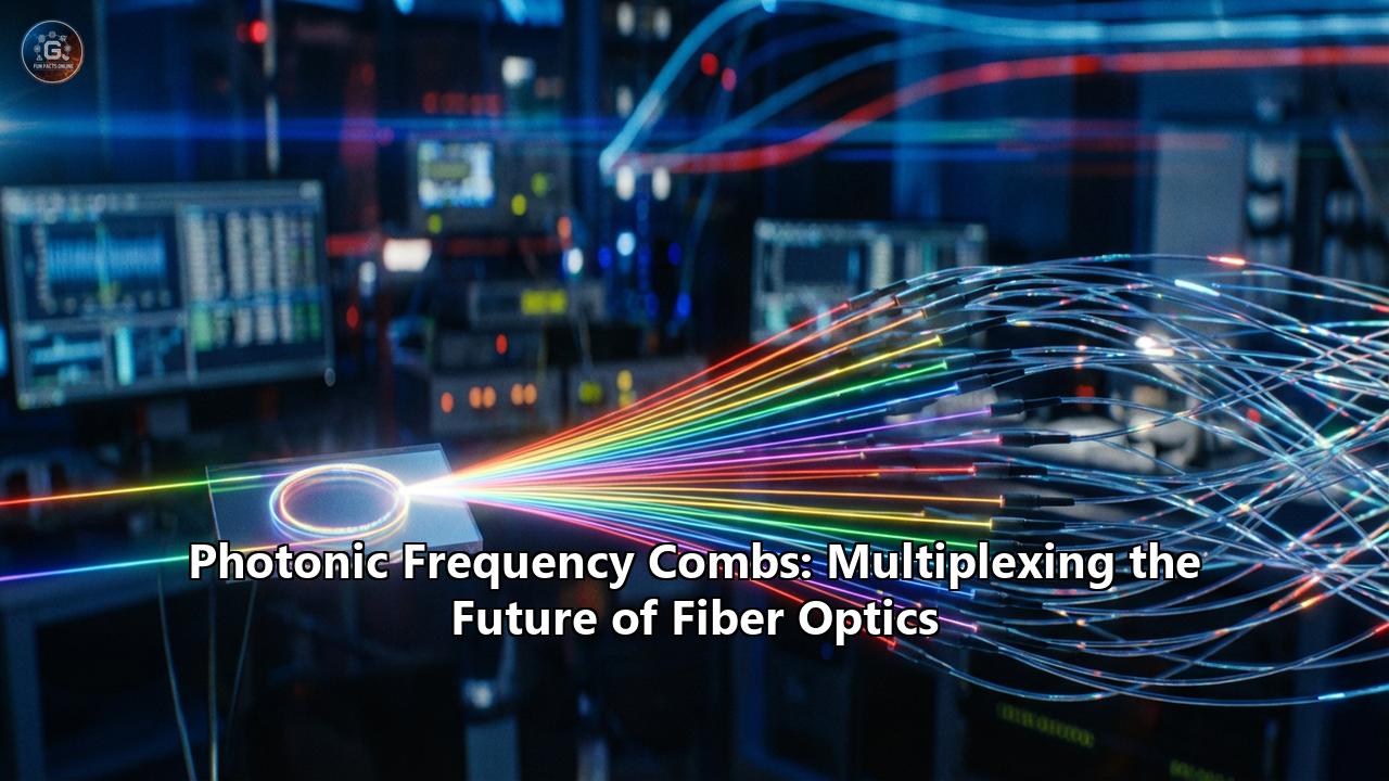
A photonic frequency comb elegant dismantles all three of these walls. Instead of using hundreds of individual lasers, a frequency comb uses a single, continuous-wave (CW) pump laser coupled into a microscopic ring resonator—a microscopic racetrack for light, often etched from silicon nitride ($Si_3N_4$) or lithium niobate.
When the single color of pump light enters the microresonator, it begins to circle the ring millions of times per second. Through a non-linear optical phenomenon known as the Kerr effect, the intense light begins to interact with the material of the resonator itself. The refractive index of the material changes in response to the light's intensity, a process called self-phase modulation. This causes the single wavelength of light to spawn new, equidistant wavelengths through a process called four-wave mixing.
Under the right conditions of carefully engineered chromatic dispersion and precise tuning, these newly generated wavelengths phase-lock with one another, forming what are known as dissipative Kerr solitons. A soliton is a self-reinforcing wave packet that maintains its shape as it travels. In the time domain, the output of the microresonator is an endless train of ultra-short, highly stable optical pulses. In the frequency domain, it appears as a "comb"—a spectrum of dozens or hundreds of perfectly sharp, perfectly spaced spectral lines, or "teeth".
For telecommunications, the implications are breathtaking:
- Absolute Equidistance: Because all the "teeth" of the comb are generated from a single cavity and phase-locked by the same fundamental physics, the distance between each frequency channel is mathematically perfect and permanently fixed. They cannot drift independently.
- Zero Guard Bands: The immutable spacing of the comb lines means that the wasteful spectral guard bands required in traditional WDM can be entirely eliminated. Channels can be packed incredibly densely, maximizing spectral efficiency and pushing data transmission right up to the theoretical Shannon limit.
- Massive Consolidation: A single microchip, measuring just a few millimeters across, can replace hundreds of bulky, power-hungry individual lasers, acting as a singular engine for massive parallel data transmission.
Shattering Records: The Petabit-per-Second Era
The theoretical promise of frequency combs in telecommunications was tantalizing, but recent experimental breakthroughs have thrust the technology out of the realm of theory and into real-world record books.
In a landmark achievement by researchers at the Technical University of Denmark, Chalmers University of Technology, and Fujikura Ltd., a single chip-scale microcomb ring resonator was used to achieve a mind-boggling data transmission rate of 1.84 Petabits per second (Pbit/s) over a distance of 7.9 kilometers.
To put this astronomical figure into perspective: 1.84 Pbit/s is equivalent to the entire global internet bandwidth being transmitted through a single optical fiber simultaneously. It equates to downloading hundreds of millions of ultra-high-definition movies in a single second.
This monumental feat was achieved by marrying the frequency comb with another cutting-edge technology: Space Division Multiplexing (SDM). The researchers utilized a custom-engineered optical fiber containing 37 distinct cores. The single microcomb generated a stabilized "dark-pulse" Kerr frequency comb. The light from this single comb was split into 37 separate copies, one for each core. Across these cores, the comb provided 223 perfectly spaced wavelength channels. Every single channel was independently modulated with data, resulting in a staggering 8,228 distinct, parallel data streams running from a single microscopic light source.
Theoretical analyses stemming from these experiments suggest that we have not yet hit the ceiling. By combining more advanced microcomb arrays with massively parallel space-and-wavelength multiplexed systems, researchers predict that single-chip light sources could soon support capacities scaling up to 100 Pbit/s. This fundamentally rewrites the roadmap for high-capacity, long-haul, and submarine optical cable designs.
Silicon Photonics and the Holy Grail of Co-Packaged Optics
While transmitting a petabit of data in a highly controlled laboratory environment is a triumph, commercializing this technology for the bustling, heat-soaked environment of a hyperscale data center requires mastery of manufacturing and integration. This is where the synthesis of frequency combs and silicon photonics becomes the most important frontier in modern hardware engineering.
Silicon photonics leverages the established, highly scaled CMOS manufacturing infrastructure—the same foundries that print computer chips—to etch microscopic optical components (waveguides, modulators, and multiplexers) onto silicon wafers. However, silicon is notoriously poor at generating light. Therefore, the ultimate goal has been to seamlessly integrate high-power, highly stable comb light sources directly onto the silicon chip, an architecture known as Co-Packaged Optics (CPO).
Recent breakthroughs, particularly those spearheaded by research teams at Columbia University (the Lipson Group), have pushed on-chip comb integration to new heights. By employing multimode laser diodes as a high-power optical source and utilizing advanced locking mechanisms, engineers have successfully stabilized and "purified" inherently unstable laser emissions directly on the chip. The light is reshaped through integrated silicon photonic structures, feeding into nonlinear microresonators to produce high-power, multi-wavelength frequency combs without the need for cumbersome external benchtop lasers.
Furthermore, advances in hybrid integration are solving the historical challenges of this platform. Heterogeneous quantum dot mode-locked lasers are being bonded directly to silicon, providing exceptional scalability, high thermal tolerance, and massive efficiency improvements. Meanwhile, the engineering of silicon nitride ($Si_3N_4$) platforms has enabled the inclusion of integrated tunable dispersion compensation directly on the chip. Because a broad frequency comb experiences chromatic dispersion (different colors of light traveling at slightly different speeds) as it traverses optical fiber, pre-compensating for this dispersion natively on the chip allows for high-speed line rates (e.g., 50 Gb/s per channel) over long distances without complex, power-hungry digital signal processing (DSP) at the receiver.
By placing the light source, the modulators, the dispersion compensators, and the receivers onto a single monolithic die, silicon photonic frequency combs are poised to dramatically shrink optical transceivers. For the booming AI industry, where thousands of GPUs must share data with microseconds of latency, this tight system integration offers a path to optical interconnects that are exponentially faster and drastically more energy-efficient.
Greening the Internet: A Thermodynamic Revolution
The narrative of the frequency comb is not merely one of speed; it is fundamentally a story of sustainability. The internet is a massive engine of carbon emission. Data centers alone consume an estimated 1-2% of global electricity, a figure projected to skyrocket as generative AI and large language models (LLMs) proliferate. A significant portion of this energy is burned by the optical interconnects sending data between server racks, and the subsequent cooling required to manage the heat generated by thousands of discrete DFB lasers.
Replacing a transceiver's array of 100 lasers with a single, highly efficient microcomb driven by a solitary pump laser drastically alters the thermodynamic profile of a data center. By encoding independent information channels onto the distinct colors of light generated by a single Kerr comb, hyperscale data centers can transition to massively parallel terabit-scale optical interconnects that operate on a fraction of the power.
This "green" scaling is vital. Without fundamentally more energy-efficient technologies, the growth of computational power will be bottlenecked by the limits of municipal power grids and thermal cooling physics. The integrated microcomb provides a crucial release valve for this pressure, ensuring that the exponential scaling of artificial intelligence computing can continue without demanding an unsustainable environmental toll.
Beyond Telecommunications: The Ripple Effect of the Optical Ruler
While multiplexing data is currently the most lucrative commercial driver for photonic frequency combs, the ultra-precise nature of these "optical rulers" has triggered a renaissance across multiple scientific and industrial domains. The perfect equidistance of their spectral lines makes them an unparalleled tool for any technology reliant on the manipulation or measurement of light.
1. Astrophotonics and the Hunt for ExoplanetsIn the realm of astrophysics, detecting Earth-like exoplanets requires observing the infinitesimal "wobble" of a distant star caused by the gravitational pull of orbiting planets. This wobble manifests as an incredibly subtle Doppler shift in the star's light. To measure this, telescopes require spectrographs calibrated to an absolute standard. Enter the "astro-comb." Utilizing gigahertz-spaced, passively stabilized frequency combs (often spanning green to near-infrared wavelengths), astronomers can calibrate their instruments with a precision unmatched by traditional hollow-cathode calibration lamps. These chip-scale astro-combs allow for the detection of radial velocity shifts down to centimeters per second, unlocking the ability to find smaller, more distant worlds in the cosmos.
2. Quantum Communications and CryptographyAs quantum computing matures, the threat to traditional encryption grows. Quantum Key Distribution (QKD) promises unbreakable cryptographic keys encoded in the quantum states of individual photons. Recent proof-of-concept architectures have successfully demonstrated the integration of QKD with Dense Wavelength Division Multiplexing (DWDM) using comb technology. By utilizing the pristine, locked channels of a frequency comb, quantum secure communications can be scaled multiplexed over existing fiber-optic infrastructures, paving the way for a scalable, quantum-secure internet.
3. Next-Generation LiDARAutonomous vehicles and advanced topographical mapping rely on Light Detection and Ranging (LiDAR) to create 3D maps of their surroundings. Traditional mechanically sweeping LiDAR systems are bulky and prone to mechanical failure. Photonic frequency combs enable Frequency-Modulated Continuous-Wave (FMCW) LiDAR on a chip. By utilizing the multiple coherent wavelengths of the comb, a single solid-state chip can emit massive parallel arrays of light beams, simultaneously measuring both the distance and instantaneous velocity of thousands of points in real-time, all with sub-millimeter precision.
4. High-Resolution Spectroscopy and Chemical SensingBecause every molecule absorbs light at a unique set of specific wavelengths, analyzing the light that passes through a gas or liquid can reveal its chemical makeup. Dual-comb spectroscopy, utilizing two slightly detuned frequency combs, allows for the ultra-rapid, ultra-high-resolution measurement of thousands of spectral absorption lines simultaneously. Integrated onto a chip, this enables portable, highly accurate environmental sensors for greenhouse gas monitoring, breath-analysis for non-invasive medical diagnostics, and real-time chemical hazard detection.
5. Optical Neuromorphic ComputingThe parallel nature of frequency combs is also being harnessed to completely rethink computation itself. In optical neuromorphic computing, researchers are using the distinct wavelength channels of a microcomb as individual "photonic neurons" or synapses. By passing these channels through complex, reconfigurable Mach-Zehnder interferometers etched into a silicon chip, linear algebraic operations—the foundation of modern machine learning—can be performed at the speed of light, with virtually zero power consumed during the computation process itself.
Overcoming the Final Hurdles: Engineering the Future
Despite the staggering progress, deploying chip-scale photonic frequency combs globally requires overcoming several stringent engineering challenges.
The first is conversion efficiency. When a single pump laser drives a microresonator to create a soliton comb, only a fraction of the pump light's power is converted into the actual comb teeth. While advances in high-Q (quality factor) microresonators and dark-pulse soliton generation have drastically improved these metrics, ensuring that every generated wavelength has the requisite signal-to-noise ratio (SNR) for ultra-long-haul telecom without heavy amplification remains a key area of study.
The second is polarization and dispersion management. Standard optical fibers exhibit chromatic dispersion, which stretches and distorts broad optical pulses over long distances. While on-chip tunable dispersion compensators are showing massive promise, maintaining the integrity of hundreds of multiplexed channels across thousands of kilometers of trans-oceanic cable requires exquisite management of both dispersion and nonlinear phase shifts.
The third is foundry scalability. Transitioning from "hero experiments" in university labs to mass production requires high-yield CMOS fabrication. The microscopic ring resonators must be etched with sub-nanometer precision; even an atom-layer difference in the waveguide wall can alter the chromatic dispersion profile, preventing the formation of stable solitons. The semiconductor industry is actively investing in new silicon nitride and thin-film lithium niobate fabrication nodes to standardize and scale the production of these complex chips.
Conclusion: The Light that Binds the Future
We stand at the precipice of a new era in optical communications. The relentless, insatiable demand for bandwidth driven by an increasingly interconnected and artificially intelligent world has forced our hand, demanding an evolution from legacy lasers to the symphony of the soliton.
The photonic frequency comb is not merely a component; it is an architectural revolution. By allowing us to multiplex hundreds of perfectly synchronized data channels from a single microscopic ring, it provides a master key to the "capacity crunch." It promises a future where petabit-per-second data streams flow effortlessly across oceans, where hyperscale AI data centers operate with drastically reduced power footprints, and where the boundaries of quantum communication, autonomous navigation, and astrophysics are continually expanded.
What began as a brilliant method to measure the fundamental tickings of the universe has now become the very heartbeat of its communication network. As research institutions and silicon foundries unite to perfect on-chip integration, the photonic frequency comb stands ready to illuminate the darkest fibers of our global infrastructure, multiplexing a faster, greener, and infinitely more connected future.
Reference:
- https://optics.conferenceseries.com/abstract/2016/chip-scale-optical-frequency-combs-advances-in-precision-metrology
- https://www.semanticscholar.org/paper/Petabit-per-second-data-transmission-using-a-ring-Photonics-J%C3%B8rgensen/40c99569c02204b0c86beaabbeef63a5237f936c
- https://orbit.dtu.dk/en/publications/petabit-per-second-data-transmission-using-a-chip-scale-microcomb/
- https://www.trendforce.com/news/2025/10/16/news-silicon-photonics-breakthrough-high-power-frequency-comb-achieved-on-chip/
- https://spoc.dtu.dk/spoc-highlights/spoc-highlights/data-transmission-record
- https://www.spiedigitallibrary.org/conference-proceedings-of-spie/13374/133740A/On-chip-comb-light-source-integration-in-silicon-photonics/10.1117/12.3044389.full
- https://preprints.opticaopen.org/articles/preprint/Optical_Kerr_microcombs_for_ultra-high_bandwidth_communications/28888559
- https://repository.kaust.edu.sa/items/e146f66d-237c-4641-8224-21cea7d7d9c6
- https://ieeexplore.ieee.org/document/10543847/
- https://arxiv.org/abs/2109.10297
- https://www.researchgate.net/figure/Overall-spectrum-of-the-astro-comb-The-spectrum-mainly-covers-from-530nm-to-560nm-where_fig4_349514927
- https://www.photondelta.com/news/