Beyond the Lens: How Flat Optics Are Revolutionizing Our World
Imagine a world where bulky camera lenses are replaced by paper-thin sheets, where augmented reality glasses are indistinguishable from everyday eyewear, and where microscopic medical imaging devices can navigate the human body with unparalleled precision. This isn't science fiction; it's the rapidly unfolding reality powered by nanostructured optical metasurfaces – a revolutionary technology that's teaching us to sculpt light in ways previously thought impossible.
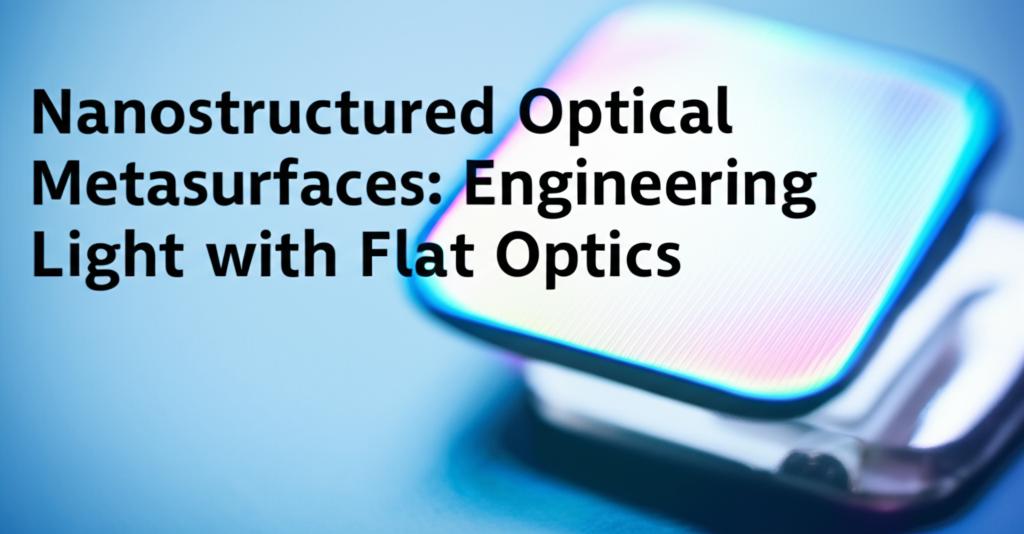
For centuries, we've relied on the gentle curves of lenses and prisms to bend and redirect light. But metasurfaces are throwing out the old playbook. These aren't your grandma's optics; they are ultra-thin, engineered materials adorned with intricate, subwavelength patterns of "nano-antennas." Think of them as a microscopic orchestra, where each tiny antenna is precisely designed to interact with light waves, collectively dictating their phase, amplitude, polarization, and even propagation direction. This unprecedented control allows scientists and engineers to craft "flat optics" that can perform the same tasks as their bulky, traditional counterparts – and often much more – within a sliver of material.
The implications are staggering and touch nearly every facet of modern technology. In imaging and sensing, metasurfaces are paving the way for super-resolution microscopy, capable of peering beyond the diffraction limit of light to reveal cellular structures in exquisite detail. Compact, single-shot polarization imaging systems built with metasurfaces are replacing complex traditional setups, promising real-time applications in medical diagnostics, like live tissue microscopy and non-invasive cancer detection. Beyond the visible, these engineered surfaces are enhancing biosensing and gas detection, offering higher sensitivity and the potential for miniaturized, portable devices.
Augmented and virtual reality (AR/VR) are poised for a massive leap forward thanks to metasurfaces. Current AR/VR headsets are often clunky and offer a limited field of view. Metasurfaces promise to deliver lightweight, high-resolution displays with wide viewing angles, making a truly immersive digital experience more accessible. Researchers are even developing metasurface-based near-eye displays that can dynamically switch between AR and VR modes, offering unparalleled flexibility. Imagine smart contact lenses that seamlessly overlay information onto your vision or gaming experiences so realistic they blur the line between the digital and physical.The magic of metasurfaces also extends to optical communication and computing. By enabling precise beam steering and polarization control, they can lead to faster and more reliable data transmission. Metasurface-integrated photodetectors can capture more complex light information, driving progress in optical computing and even enabling tasks like edge detection for image processing.
One of the most exciting frontiers is the development of tunable and reconfigurable metasurfaces. Imagine optical components that can change their function on demand, adapting to different lighting conditions or a user's specific needs. By incorporating materials that respond to external stimuli like temperature or electricity, researchers are creating dynamic metasurfaces that can switch between, for instance, high-contrast edge detection and detailed infrared imaging. This adaptability opens doors for highly versatile sensors and optical systems that can learn and evolve.
Furthermore, the flat nature of metasurfaces makes them inherently compatible with established semiconductor manufacturing techniques. This is a crucial factor for bringing this groundbreaking technology out of the lab and into consumer devices. While challenges in large-scale, cost-effective manufacturing remain, significant progress is being made, paving the way for the widespread commercialization of metasurface-based photonic devices. Companies are already beginning to integrate metasurface technology into commercial products, such as sensors for smartphones and other consumer electronics.
The journey of nanostructured optical metasurfaces is just beginning. From revolutionizing healthcare diagnostics and consumer electronics to pushing the boundaries of renewable energy and quantum technologies, these "flat optics" are reshaping our interaction with light. As research continues to unlock new functionalities and fabrication techniques mature, we can expect metasurfaces to become increasingly integrated into the fabric of our technological world, leading to a future where powerful optical tools are more compact, efficient, and versatile than ever before. The ability to engineer light at the nanoscale is not just a scientific curiosity; it's a pathway to a brighter, more connected, and more insightful future.