The era of the backlight is ending. For decades, the dominant paradigm in display technology—Liquid Crystal Displays (LCD)—relied on a fundamental compromise: a passive layer of liquid crystals acting as light valves to block or transmit light from a generic, always-on backlight unit. This architecture, while mature and cost-effective, is bound by the laws of physics to suffer from light leakage, limited contrast, and wasted energy. The future belongs to self-emissive technologies, where every single sub-pixel is its own independent light source.
Two titans now stand at the forefront of this revolution: OLED (Organic Light Emitting Diode) and MicroLED (often referred to as Micro RGB in its pure inorganic form). While they share the superficial similarity of being self-emissive, their underlying physics are diametrically opposed. One relies on the soft, complex chemistry of organic molecules and the statistical management of excitonic spin states. The other harnesses the hard, crystalline certainty of inorganic semiconductors and band-to-band recombination.
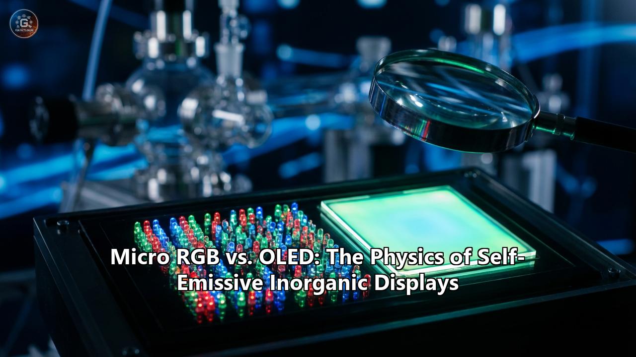
This comprehensive analysis explores the deep physics, manufacturing thermodynamics, and optical engineering that define the battle between Micro RGB and OLED.
Part I: The Physics of Emission
To understand the divergence between these technologies, we must first look at the quantum mechanical events that generate a photon in each system.
1. Organic Electroluminescence: The Exciton Challenge
OLED technology is built upon organic semiconductors—carbon-based molecules that possess a conjugated $\pi$-electron system. In these molecules, carbon atoms bond via $sp^2$ hybridization, leaving one $p_z$ orbital perpendicular to the molecular plane. These orbitals overlap to form delocalized $\pi$ (bonding) and $\pi^$ (antibonding) molecular orbitals.
In the language of solid-state physics, the Highest Occupied Molecular Orbital (HOMO) serves as the valence band, and the Lowest Unoccupied Molecular Orbital (LUMO) serves as the conduction band. When a voltage is applied, electrons are injected into the LUMO from the cathode, and holes are injected into the HOMO from the anode.
The Spin Statistics ProblemWhen an electron and a hole meet in an organic molecule, they form a bound state called an exciton. Unlike free carriers in inorganic crystals, these excitons are strongly localized Frenkel excitons with high binding energy (0.5 – 1.0 eV). The crucial physics limitation here is quantum mechanical spin.
Electrons and holes are fermions with spin $1/2$. When they combine, their spins can align in two ways:
- Singlet State ($S=0$): Spins are anti-parallel ($\uparrow \downarrow$). This state decays rapidly (nanoseconds) via fluorescence, emitting a photon.
- Triplet State ($S=1$): Spins are parallel ($\uparrow \uparrow$). Radiative decay from a triplet to a singlet ground state is "forbidden" by selection rules because it requires a spin flip, which is highly improbable without external perturbation.
According to spin statistics, the combination of uncorrelated electrons and holes results in a ratio of 1:3 for Singlets to Triplets.
- 1st Gen OLED (Fluorescence): Only harvested Singlets. Max Internal Quantum Efficiency (IQE) = 25%. The remaining 75% of energy was lost as heat.
- 2nd Gen OLED (Phosphorescence - PHOLED): Introduced heavy metal atoms (like Iridium or Platinum) into the molecule. The strong spin-orbit coupling of the heavy nucleus mixes the singlet and triplet states, making the "forbidden" transition allowed. This unlocks 100% IQE but suffers from stability issues, particularly in blue emitters.
- 3rd Gen OLED (TADF): Thermally Activated Delayed Fluorescence. These molecules are designed with a very small energy gap ($\Delta E_{ST}$) between the Singlet and Triplet states. Thermal energy at room temperature is sufficient to "upconvert" Triplet excitons back into Singlet states via Reverse Intersystem Crossing (RISC), allowing them to emit light as delayed fluorescence.
The "Blue Problem" in OLEDs is a direct consequence of the high energy of blue photons (~2.8 eV). In PHOLEDs, the long lifetime of triplet excitons leads to a high density of excited states. When two excitons collide (Triplet-Triplet Annihilation), their combined energy can exceed the bond dissociation energy of the organic molecule (typically C-N or C-C bonds), literally breaking the molecule apart. This photochemical degradation is why blue OLED pixels die faster than red or green, necessitating the "Pentile" sub-pixel arrangement where blue pixels are made physically larger to reduce current density.
2. Inorganic Electroluminescence: Band-to-Band Recombination
MicroLEDs abandon organic chemistry in favor of the wurtzite crystal structure of Group III-Nitrides (GaN, InGaN) and Zincblende III-Phosphides (AlGaInP).
Here, light emission is not excitonic but arises from band-to-band recombination of free carriers.
- Band Structure: In a direct bandgap semiconductor like Gallium Nitride (GaN), the minimum of the conduction band and the maximum of the valence band occur at the same crystal momentum ($k=0$).
- Recombination: An electron drops from the conduction band to the valence band, annihilating a hole and releasing energy equal to the bandgap ($E_g$) as a photon ($E = h\nu$).
- Robustness: The binding energy of the atoms in a GaN crystal is vastly higher than in organic molecules. There are no weak C-H bonds to break. A MicroLED can run at current densities $1000\times$ higher than an OLED without immediate degradation.
While robust, III-Nitride LEDs face their own physics demons. GaN is a polar material. When grown on mismatched substrates (like Sapphire or Silicon), strain induces huge internal piezoelectric fields. These fields tilt the energy bands in the quantum wells, spatially separating the electron and hole wavefunctions. This reduces the probability of recombination, a phenomenon known as the Quantum Confined Stark Effect. This is particularly bad for Green and Red InGaN LEDs, where high Indium content creates massive strain—a major hurdle for "True RGB" MicroLEDs.
Part II: The Manufacturing Physics Barrier
If MicroLED is physically superior in brightness and lifespan, why does OLED dominate the market? The answer lies in the physics of mass manufacturing.
1. OLED: The Thermodynamics of Evaporation
The standard manufacturing process for high-end OLEDs (like in iPhones) is Vacuum Thermal Evaporation (VTE) through a Fine Metal Mask (FMM).
- Knudsen Number Regime: VTE operates in a high vacuum where the mean free path of the molecules is longer than the chamber dimensions (Knudsen number $Kn > 1$). Organic molecules travel in straight ballistic lines from the crucible to the substrate.
- The Shadow Mask Limit: To define pixels, a metal mask with tiny holes is placed close to the substrate. However, the mask cannot be infinitely thin (it would sag) or infinitely close (it would scratch). This creates a "shadowing" effect that limits pixel density. Furthermore, the mask heats up from the hot vapor, expanding thermally. This thermal expansion mismatch limits the size of the glass substrate (Gen 6 is the current limit for FMM), making OLED TVs expensive to produce using RGB patterning.
To scale up, manufacturers are trying inkjet printing. Here, the physics shifts from ballistics to fluid dynamics.
- The Coffee-Ring Effect: When a droplet of ink dries, evaporation is faster at the pinned contact line (the edge). Capillary flow rushes liquid from the center to the edge to replenish the loss, carrying the organic solute with it. This results in a pixel with thick edges and a thin center—terrible for uniform emission.
- Marangoni Flow: Engineers must manipulate the Marangoni effect—mass transfer driven by surface tension gradients. By using a mix of solvents with different boiling points and surface tensions, they can induce a recirculating flow inside the drying droplet that counteracts the coffee-ring effect, redistributing the material to form a flat, uniform "U-shape" profile.
2. MicroLED: The Van der Waals Challenge
MicroLEDs are grown on 4-inch or 8-inch wafers, but a TV requires them to be spread out over 65+ inches. This requires Mass Transfer: picking up millions of microscopic chips (smaller than a grain of pollen) and placing them precisely on a backplane.
The physics problem here is that at the micro-scale ( < 10 µm), gravity becomes irrelevant, and surface forces dominate.
- Van der Waals Forces: These are weak intermolecular attractive forces that scale with contact area. For a tiny MicroLED, the van der Waals attraction to its donor wafer is incredibly strong relative to its weight.
- Viscoelastic Adhesion (The Gecko Effect): The leading solution uses elastomer stamps (PDMS). The adhesion of these stamps is rate-dependent.
High Velocity Pull: The polymer chains don't have time to relax, making the stamp stiff and the fracture energy high. Adhesion is strong (Pick up).
Low Velocity Peel: The chains relax, the interface behaves like a viscous liquid. Adhesion is weak (Drop off).
This kinetic control allows the transfer of millions of LEDs with 99.9999% yield, but the "speed limit" of this physical process fundamentally dictates the cost of the display.
Part III: The "True RGB" vs. Color Conversion Dilemma
One of the fiercest debates in the MicroLED world is how to generate color.
Approach A: True RGB (Inorganic)
Use separate Red, Green, and Blue semiconductor blocks.
- Blue/Green: Made from Indium Gallium Nitride (InGaN).
- Red: Typically made from Aluminum Gallium Indium Phosphide (AlGaInP).
AlGaInP has a fatal flaw at the micro-scale. It has a very high Surface Recombination Velocity ($10^6$ cm/s). When you shrink a red LED to < 10 µm, the ratio of surface area to volume skyrockets. Carriers (electrons/holes) diffuse to the sidewalls and are trapped by surface defects before they can recombine radiatively. This causes the efficiency of red MicroLEDs to plummet below 5% at small sizes, while blue remains near 40-50%.
Approach B: Blue + Quantum Dot Color Conversion (QD-CC)
Use only Blue MicroLEDs (which are efficient and easy to make) and print a layer of Quantum Dots (QDs) on top to convert Blue to Red and Green.
The Physics of Quantum DotsQDs are semiconductor nanocrystals where the exciton wavefunction is confined in all three spatial dimensions. This Quantum Confinement means the bandgap is tunable by simply changing the size of the particle (smaller = bluer, larger = redder).
- Stokes Shift Engineering: A major challenge is Self-Absorption. If a QD emits a photon, a neighboring QD of the same size might re-absorb it. This photon recycling leads to losses. Advanced QDs use a "Core-Shell" structure (e.g., InP core, ZnS shell). By designing a Type-II band alignment, the electron and hole are spatially separated, inducing a large Stokes Shift (a gap between absorption and emission peaks). This ensures that once a photon is emitted, it cannot be re-absorbed by the QD layer, preserving efficiency.
- Blue Leakage: The physics challenge here is optical density. The blue light must be fully absorbed by the thin QD layer. If blue photons leak through the red pixel, color purity is ruined. This requires extremely high absorption coefficients or Distributed Bragg Reflectors (DBR) to recycle the blue light until it is converted.
Part IV: System-Level Physics – Crosstalk and Contrast
1. OLED: Electrical Crosstalk
In high-resolution OLED microdisplays (like those in the Apple Vision Pro), pixels are so close that they share common organic layers (Hole Injection/Transport Layers) to save cost. This creates a path for Lateral Leakage Current. Current intended for one pixel can drift sideways through the conductive organic layers to light up a neighbor. This "Electrical Crosstalk" blurs the image and reduces color gamut.
2. MicroLED: Optical Crosstalk
MicroLEDs are distinct islands, so electrical crosstalk is negligible. However, they are essentially tiny omnidirectional light bulbs. Without proper isolation, photons emitted sideways from a blue pixel can travel through the glass substrate and exit through a neighboring red pixel.
- The Solution: Deep Trench Isolation (DTI). Physical barriers must be etched between pixels and filled with reflective metal or absorbing black matrix material. The physics of Total Internal Reflection (TIR) within the encapsulation layers also must be managed to extract light toward the viewer rather than trapping it in waveguide modes.
Part V: The Future – Porous GaN and Nanostructuring
The most exciting recent development (2024-2025) in MicroLED physics is the use of Nanoporous GaN.
By electrochemically etching the GaN wafer, engineers can create a sponge-like structure full of nanopores.
- Strain Relief: The porous structure is mechanically compliant. It acts as a stress-relief layer, allowing high-Indium (Red) InGaN layers to be grown on top without the massive strain that usually destroys efficiency. This could finally solve the "Green Gap" and enable efficient InGaN Red MicroLEDs, eliminating the need for the problematic AlGaInP material.
- Light Extraction: The refractive index of porous GaN can be tuned by changing the porosity. This allows the creation of built-in Distributed Bragg Reflectors (DBRs) underneath the LED, reflecting light upward that would otherwise be lost into the substrate.
Conclusion: The Winner?
OLED remains the master of the "soft" physics regime. It is mature, manufacturable on flexible substrates, and its contrast is infinite. However, it is fundamentally limited by the chemical stability of organic bonds and the excitonic spin statistics. Micro RGB is the master of the "hard" physics regime. Its inorganic crystal lattice offers nearly practically infinite lifespan and blinding brightness (millions of nits). The challenges are not in the fundamental device physics, but in the manufacturing physics—specifically the thermodynamics of mass transfer and the surface recombination at micro-scales.As we move toward 2030, the boundaries will blur. Quantum Dots are bridging the gap, and porous semiconductors are solving the strain issues. But for now, MicroLED represents the ultimate "Physics Dream" of a display: a direct connection between electricity and light, unmediated by liquid crystals or fragile organic molecules.
Deep Dive Sections
A. The Thermodynamic War: Heat Dissipation
A critical but often overlooked difference is thermal physics.
- OLED: Organic materials are thermal insulators. Heat generated in the center of a panel gets trapped, accelerating degradation (Arrhenius equation). This limits peak brightness.
- MicroLED: GaN is a decent thermal conductor, and it is usually bonded to a silicon or metal backplane. This allows MicroLEDs to be driven at massive current densities. The heat is wicked away efficiently, allowing for sustained brightness levels that would literally cook an OLED.
B. The Eye and the Artifact: Response Time Physics
- OLED: Response time is $< 0.1$ ms. However, most OLEDs use "Sample and Hold" driving, which causes motion blur due to the persistence of vision in the human eye/brain system, not the display itself.
- MicroLED: The recombination lifetime in GaN is in the nanosecond range ($10^{-9}$ s). This incredible speed opens up new physics domains, such as Li-Fi (transmitting data via visible light communication) directly from the display pixels, turning a TV into a multi-gigabit wireless transmitter—something physically impossible for the slow relaxation of organic excitons.
C. The Transparency Factor
MicroLEDs occupy a tiny fraction of the pixel area (often < 1% fill factor). The rest is empty space. In OLEDs, the TFT circuitry and organic layers cover more area.
This makes MicroLED the king of Transparent Displays. Physically, light can pass through the empty gaps between the microscopic emitters with almost no diffraction, enabling heads-up displays (HUDs) and AR glasses with transparency > 90%, merging the digital and physical worlds in a way that is dictated by the diffraction limits of the emitter grid pitch.
(End of Article Summary)*Reference:
- https://pubs.aip.org/aip/apr/article/11/2/021319/3293967/Recent-advances-in-micro-pixel-light-emitting
- https://www.researchgate.net/publication/301303821_Impact_of_surface_recombination_on_efficiency_of_III-nitride_light-emitting_diodes
- https://par.nsf.gov/servlets/purl/10603864
- https://gg.mit.edu/wp-content/uploads/2018/03/acsnano.8b00132.pdf
- https://pubs.acs.org/doi/10.1021/acsami.7b19144
- https://en.wikipedia.org/wiki/Stokes_shift
- https://pmc.ncbi.nlm.nih.gov/articles/PMC10462745/
- https://www.sciencedaily.com/releases/2025/12/251205054734.htm
- https://www.latest.com/perovskite-leds-shine-as-top-innovation-in-display-tech