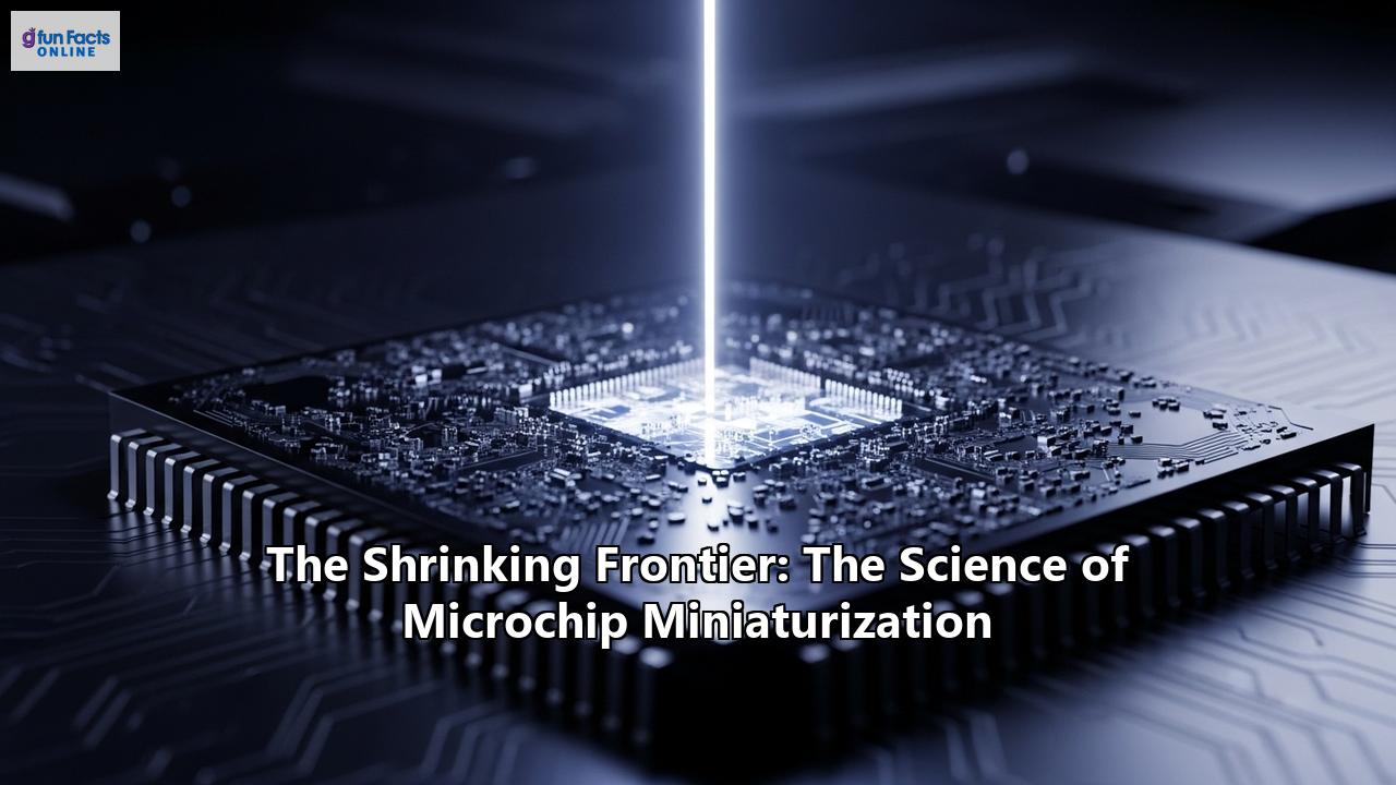
The Incredible Shrinking Frontier: A Deep Dive into the Science of Microchip Miniaturization
The world as we know it runs on the minuscule, the microscopic, the practically invisible. From the supercomputers charting the vastness of space to the smartphones nestled in our pockets, a silent revolution has been raging for over half a century – a relentless quest to shrink the fundamental building block of modern electronics: the transistor. This journey into the nanoscopic realm, a process known as microchip miniaturization, has been the engine of the digital age, a primary driver of technological progress that has reshaped society in countless ways. But this frontier is shrinking, and the path forward is fraught with physical limits and monumental economic challenges. This is the story of that shrinking frontier, the science that has propelled us to its very edge, and the innovations that promise to carry us beyond.
The Prophecy of a Self-Fulfilling Law
The saga of microchip miniaturization is inextricably linked to a prediction made in 1965 by Gordon Moore, a co-founder of Intel. In an article for Electronics magazine, Moore observed that the number of components on an integrated circuit had been doubling approximately every year since their invention in 1958. He boldly predicted this trend would continue for at least another decade. In 1975, he revised this forecast to a doubling of transistors every two years. This observation, which became known as "Moore's Law," was not a law of physics but rather an empirical trend and a projection of a historical pattern.
However, Moore's Law became more than just an observation; it evolved into a self-fulfilling prophecy, a North Star for the entire semiconductor industry. It set a daunting, yet clear, roadmap for researchers, engineers, and companies, challenging them to innovate at a breakneck pace. This relentless pursuit of Moore's Law has been the primary driver of the exponential growth in computing power and the simultaneous decrease in cost. Every two years, we could expect computers to become roughly twice as powerful for the same price, a phenomenon that has fueled innovation in countless fields, from medicine and communication to entertainment and transportation.
The heart of Moore's Law lies in the miniaturization of transistors, the tiny electrical switches that form the basis of all digital logic. These transistors, arranged by the billions on a small piece of silicon, control the flow of electricity, representing the ones and zeros of the binary language that underpins all computation. By shrinking transistors, more can be packed onto a single chip, leading to increased processing power, improved energy efficiency, and lower manufacturing costs per transistor.
The Art of Building the Infinitesimally Small: A Symphony of Precision
The creation of a modern microchip is a marvel of manufacturing, a complex ballet of physics and chemistry performed in some of the most sterile environments on Earth – fabrication plants, or "fabs." The general process involves taking a thin slice of a large, single-crystal silicon ingot, called a wafer, and building up intricate, multi-layered structures of transistors and the metallic wires that connect them. This is achieved through a series of fundamental processes repeated dozens, sometimes hundreds, of times.
From Sand to Silicon Wafer
The journey begins with a surprising raw material: sand. Specifically, silica sand, which is primarily composed of silicon dioxide. This sand is purified and melted at extremely high temperatures to produce high-purity, electronics-grade silicon. This molten silicon is then carefully grown into a large, cylindrical single crystal known as a boule. These boules are then sliced into thin, highly polished wafers, typically 300mm (about 12 inches) in diameter, which serve as the pristine canvases upon which the intricate circuitry of a microchip will be "painted."
Photolithography: Painting with Light
At the heart of microchip manufacturing is photolithography, a process that, as its name suggests, uses light to transfer a pattern onto the silicon wafer. This technique is the key to creating the incredibly complex and minuscule features of a modern processor. The process begins by coating the wafer with a light-sensitive material called a photoresist.
A photomask, which is a sort of stencil of the desired circuit pattern, is then placed between a light source and the wafer. When exposed to light, typically deep ultraviolet (DUV) or, in the most advanced processes, extreme ultraviolet (EUV) light, the chemical structure of the photoresist changes in the exposed areas. Depending on the type of photoresist used (positive or negative), either the exposed or unexposed portions become soluble. A developer solution is then used to wash away the soluble photoresist, leaving behind a patterned layer that mirrors the design on the photomask. This process is repeated for each layer of the chip, with each new mask pattern precisely aligned with the previous ones.
The resolution of photolithography, meaning the smallest feature size it can create, is directly related to the wavelength of the light used. For decades, the industry has pushed to shorter and shorter wavelengths of light to print smaller and smaller transistors.
Etching: Sculpting the Circuits
Once the photoresist pattern is in place, the next step is etching. This process selectively removes material from the wafer in the areas not protected by the photoresist, effectively sculpting the circuit components and interconnects into the underlying layers. There are two primary methods of etching:
- Wet Etching: This technique uses liquid chemicals, or etchants, to dissolve the exposed material. While relatively simple and inexpensive, wet etching is isotropic, meaning it etches in all directions, which can undercut the photoresist and limit the precision of the features.
- Dry Etching: In modern semiconductor fabrication, dry etching, also known as plasma etching, is the dominant method. This process uses a plasma, an ionized gas, to bombard the wafer's surface. The high-energy ions and reactive chemical species in the plasma remove material with much greater directionality (anisotropy) than wet etching, allowing for the creation of the vertical, well-defined features required for today's minuscule transistors. Reactive Ion Etching (RIE) is a common form of dry etching that combines physical sputtering with chemical reactions to achieve high precision.
After the etching is complete, the remaining photoresist is stripped away, leaving the desired pattern permanently etched into the wafer layer.
Deposition: Building the Chip Layer by Layer
To build the complex, three-dimensional structure of a microchip, various materials must be added to the wafer in thin, uniform layers. This process is called deposition. These layers can be conductive (like copper or aluminum, to form the wiring), insulating (like silicon dioxide, to prevent short circuits), or semiconducting. The primary deposition techniques are:
- Physical Vapor Deposition (PVD): This is a process where a material is vaporized, either through heating (evaporation) or by bombarding it with ions (sputtering), and then condensed onto the wafer's surface to form a thin film.
- Chemical Vapor Deposition (CVD): In this method, the wafer is exposed to one or more volatile precursor gases, which react and/or decompose on the substrate surface to produce the desired thin film.
- Atomic Layer Deposition (ALD): A more advanced technique, ALD builds up material one atomic layer at a time by exposing the surface to sequential, self-limiting chemical reactions. This allows for exceptional control over film thickness and uniformity, which is crucial for the most advanced chip designs.
These three core processes – photolithography, etching, and deposition – are repeated in a carefully choreographed sequence to build up the billions of transistors and their intricate network of connections that make up a modern microchip.
The Evolution of the Transistor: From Planar to 3D
The workhorse of the digital age has been the Complementary Metal-Oxide-Semiconductor (CMOS) transistor. CMOS technology uses pairs of p-type and n-type Metal-Oxide-Semiconductor Field-Effect Transistors (MOSFETs) to create logic gates. In a CMOS inverter, for example, when the input is high, the n-type MOSFET turns on and the p-type MOSFET turns off, pulling the output low. Conversely, when the input is low, the p-type turns on and the n-type turns off, pulling the output high. A key advantage of CMOS is its low static power consumption, as one of the transistors in the pair is always off, except for the brief moment of switching.
For many years, transistors were planar, meaning their components were laid out flat on the surface of the silicon. However, as these planar transistors shrank, they began to suffer from undesirable "short-channel effects." The primary issue was current leakage. As the distance between the source and drain of the transistor became incredibly small, the gate's control over the channel weakened, and electrons could "leak" through even when the transistor was supposed to be off. This leakage current wasted power and generated excess heat.
To combat these problems, the industry made a revolutionary shift to a three-dimensional transistor architecture known as the FinFET (Fin Field-Effect Transistor), first commercialized in the early 2010s. In a FinFET, the channel between the source and drain is raised into a three-dimensional "fin." The gate is then wrapped around this fin on three sides. This multi-gate structure provides much better electrostatic control over the channel, significantly reducing leakage current and allowing for faster switching speeds.
But the relentless march of miniaturization continues, and even FinFETs are reaching their limits at the 5nm and 3nm nodes. As the fins become narrower to pack more transistors, their ability to drive current diminishes, and leakage through the uncontrolled bottom of the fin becomes a problem.
This has led to the development of the next evolution in transistor design: the Gate-All-Around (GAA) FET. As the name implies, the gate material in a GAA transistor completely surrounds the channel on all four sides. Early implementations of GAAFETs use horizontally stacked "nanosheets" or "nanowires" to form the channel. This all-around gate provides superior electrostatic control compared to the three-sided gate of a FinFET, further reducing leakage and enabling continued scaling to the 3nm node and beyond. Samsung has already begun manufacturing chips using GAA technology, with other major foundries like TSMC expected to follow suit.
The Shrinking Frontier: Pushing Against the Laws of Physics
For decades, the semiconductor industry has successfully navigated the challenges of miniaturization. However, as transistors shrink to sizes measured in just a few nanometers – approaching the scale of individual atoms – we are beginning to collide with the fundamental laws of physics.
The Quantum Tunneling Problem
One of the most significant hurdles is a quantum mechanical phenomenon known as quantum tunneling. In the classical world, an object needs enough energy to overcome a barrier. However, in the quantum realm, particles like electrons exhibit wave-like properties. This means there is a non-zero probability that an electron can simply "tunnel" through a thin insulating barrier, even if it doesn't have enough energy to go over it.
In the context of transistors, the insulating gate oxide layer is designed to prevent current from flowing when the transistor is in the "off" state. As this layer becomes just a few atoms thick, electrons can tunnel through it, creating a leakage current. This not only wastes power but also makes it difficult to reliably distinguish between the "on" and "off" states of the transistor, undermining the very foundation of digital logic. At a certain point, transistors become so small that quantum tunneling makes them behave less like reliable switches and more like leaky faucets. Current estimates suggest that for silicon-based transistors, this fundamental limit lies around the 1 to 2-nanometer scale.
The Heat is On: The Power Density Challenge
Another major challenge is heat dissipation. The power consumed by a chip is ultimately converted into heat. As more and more transistors are packed into the same area, the power density – the amount of power dissipated per unit area – increases dramatically. This leads to the formation of "hotspots" on the chip, where temperatures can rise to levels that impair performance and can even cause permanent damage to the processor.
Modern high-performance CPUs can have Thermal Design Power (TDP) ratings of over 280 watts, and under heavy load, the heat generated can cause temperatures to exceed 90°C. To prevent damage, processors will engage in "thermal throttling," a self-preservation mechanism where they automatically reduce their clock speed to lower the temperature. This, of course, negates the performance benefits of having a more powerful chip in the first place.
The problem is exacerbated by the very structures that enable smaller transistors. For example, the move to 3D architectures and the thinning of the silicon substrate make it more difficult for heat to spread out and dissipate. Traditional air cooling with fans and heatsinks is becoming insufficient for high-end processors, pushing the industry towards more advanced and expensive solutions like all-in-one (AIO) liquid coolers or even more exotic custom water-cooling loops. Managing heat is no longer a secondary concern; it has become a primary bottleneck in chip design.
The Economics of the Nanoscale: A Billion-Dollar Gamble
Beyond the physical challenges, the economic realities of advanced semiconductor manufacturing are staggering. The cost of building a new, state-of-the-art fabrication plant has skyrocketed. In the early 1980s, a fab might have cost around $200 million. Today, a leading-edge fab can cost anywhere from $10 billion to $20 billion, with some projects reaching even higher figures. For example, TSMC's investment in its Arizona facilities is projected to be around $65 billion.
These astronomical costs are driven by several factors. The complexity of the manufacturing processes requires increasingly sophisticated and expensive equipment. A prime example is the Extreme Ultraviolet (EUV) lithography machine, which is essential for producing chips at the 7nm node and below. These machines, which use an incredibly short wavelength of 13.5 nm light to etch patterns, are produced by a single company, ASML, and are estimated to cost between $300 million and $400 million each.
Furthermore, the construction of the fabs themselves is a massive undertaking, requiring vast cleanroom facilities with complex air filtration and vibration control systems. Inflation and the specialized labor required for construction and operation also contribute to the escalating costs. The sheer capital investment required to stay at the cutting edge of semiconductor manufacturing has led to a consolidation of the industry, with only a handful of companies, such as TSMC, Samsung, and Intel, able to afford the price of admission to the most advanced process nodes.
Beyond the Horizon: The Future of Miniaturization
With Moore's Law slowing down and the physical and economic walls closing in, the industry is at an inflection point. The question is no longer just about making transistors smaller, but about finding new and innovative ways to continue increasing computational power and efficiency. The path forward is likely to be a multi-faceted one, combining several promising technologies.
Thinking in 3D: The Rise of Chip Stacking
One of the most promising avenues for continuing to increase transistor density is to build upwards. 3D chip stacking involves vertically integrating multiple layers of silicon chips, or "chiplets," into a single package. This allows for a much higher density of transistors in a given footprint and can significantly reduce the distance that signals have to travel between different parts of the processor. Shorter connections mean faster communication and lower power consumption.
This "chiplet" approach also offers a more modular and cost-effective way to design and manufacture processors. Instead of building one large, monolithic chip, where a single defect can render the entire chip useless, manufacturers can create smaller, specialized chiplets (e.g., a CPU chiplet, a GPU chiplet, an I/O chiplet) and then interconnect them. This can improve manufacturing yields and allow for greater design flexibility.
New Materials for a New Era
The limitations of silicon are prompting researchers to explore new materials with superior electrical properties. Some of the most promising candidates include:
- Graphene: A single layer of carbon atoms arranged in a honeycomb lattice, graphene is an incredibly strong, lightweight, and highly conductive material. Its unique properties could theoretically allow for the creation of much smaller and more energy-efficient transistors.
- Carbon Nanotubes (CNTs): These are cylindrical molecules made of rolled-up sheets of graphene. CNTs can behave as semiconductors and have the potential to be used to create transistors that are smaller and faster than their silicon counterparts. Researchers have already demonstrated that CNTs could be used to build transistors with a 1nm gate length.
- Other 2D Materials: Beyond graphene, scientists are investigating a whole class of "two-dimensional" materials, such as molybdenum disulfide (MoS2), that could be used to build next-generation transistors.
While these materials hold immense promise, there are still significant challenges to overcome in terms of manufacturing them at scale and integrating them into existing fabrication processes.
A New Architecture for a New Age: The Rise of Specialization
For decades, the Central Processing Unit (CPU) has been the versatile "brain" of most computing devices. However, as the gains from general-purpose computing slow down, there is a growing trend towards specialized hardware designed to excel at specific tasks.
- Graphics Processing Units (GPUs): Originally designed for rendering graphics, GPUs have proven to be exceptionally well-suited for the parallel processing required for tasks like scientific computing and, most notably, training artificial intelligence models.
- Tensor Processing Units (TPUs) and other AI Accelerators: Companies like Google have developed custom-designed chips specifically for the mathematical operations that are at the heart of machine learning. These AI accelerators can perform these tasks much more quickly and efficiently than a general-purpose CPU.
This shift towards specialized architectures, often combined in a single system, represents a move away from the "one-size-fits-all" approach of the past. The future of computing will likely involve a heterogeneous mix of processors, each optimized for the tasks it performs best.
The End of an Era, the Dawn of a New One
The golden age of Moore's Law, with its predictable, biennial doubling of transistor density, may be drawing to a close. The shrinking frontier of microchip miniaturization is presenting challenges that can no longer be overcome by simply making things smaller. Quantum tunneling, heat dissipation, and the astronomical cost of manufacturing are formidable barriers.
However, this is not the end of the story of computational progress. Instead, we are entering a new and exciting era of innovation. The focus is shifting from brute-force scaling to a more nuanced approach that combines advances in transistor architecture, like the move to Gate-All-Around FETs, with new ways of thinking about chip design and system architecture, such as 3D stacking and the rise of specialized processors. The exploration of new materials like graphene and carbon nanotubes holds the potential for even more radical breakthroughs in the decades to come.
The relentless drive to cram more and more computational power into smaller and smaller spaces has defined the digital age. While the path forward is more challenging than ever, the ingenuity of scientists and engineers continues to push the boundaries of what is possible. The frontier may be shrinking, but the human capacity for innovation remains boundless. The next chapter in the story of the microchip promises to be just as revolutionary as the last.
Reference:
- https://www.azonano.com/article.aspx?ArticleID=6801
- https://ttconsultants.com/advancing-microchip-technology-the-role-of-extreme-ultraviolet-lithography-euvl/
- https://www.zeiss.com/semiconductor-manufacturing-technology/inspiring-technology/euv-lithography.html
- https://semiengineering.com/getting-rid-of-heat-in-chips/
- https://www.bcg.com/publications/2023/navigating-the-semiconductor-manufacturing-costs
- https://www.researchgate.net/publication/253667355_Physical_limits_for_scaling_of_integrated_circuits
- https://research.ibm.com/blog/what-is-euv-lithography
- https://www.quora.com/How-does-quantum-tunneling-affect-the-performance-of-modern-transistors-and-what-are-the-implications-for-future-semiconductor-design
- https://www.computer.org/csdl/magazine/co/2024/08/10632608/1ZgY9Z1kif6
- https://www.quora.com/How-much-does-it-cost-to-build-a-semiconductor-fabrication-plant-How-long-does-it-take-to-build-one
- https://medium.com/@markveerasingam/quantum-tunneling-the-semiconductors-struggle-in-the-miniaturization-race-7ef2df8f9e48
- https://www.quora.com/Is-there-a-physical-limit-we-know-of-for-silicon-based-CPUs-Meaning-how-small-can-we-get-before-we-hit-a-limit-4-nm-Lower
- http://www.fisica.unipg.it/~luca.gammaitoni//fisinfo/documenti-fisici/physical-limits-silicon.pdf
- https://en.wikipedia.org/wiki/Quantum_tunnelling
- https://hsetdata.com/index.php/ojs/article/view/947
- https://eureka.patsnap.com/report-optimize-quantum-tunneling-effects-for-faster-transistors
- https://www.reddit.com/r/computerscience/comments/1f5zwnu/at_what_point_will_we_reach_the_limit_of_computer/
- https://www.chetanpatil.in/the-hidden-costs-of-generating-semiconductor-data-understanding-the-global-economic-impact-and-the-need-for-open-access/
- https://www.researchgate.net/publication/231030591_Physical_limits_of_silicon_transistors_and_circuits
- http://www.measure.jp/B/product/burn_in_func/20080607EADS-Burn-In-Intro/img/Intel-NextGenerationBurnIinSystem.pdf
- https://www.engicam.com/art/223072/formidable-adversary-HEAT
- https://www.researchgate.net/publication/262373650_Thermal_Performance_and_Key_Challenges_for_Future_CPU_Cooling_Technologies
- https://aditya-sunjava.medium.com/how-cooling-and-memory-limitations-impact-massive-multi-core-cpus-in-personal-computers-66042bda51aa
- https://en.wikipedia.org/wiki/Extreme_ultraviolet_lithography