The human eye is an evolutionary marvel, yet it is profoundly blind. It operates at a sluggish frame rate of about 10 to 100 milliseconds, and it can only perceive a tiny sliver of the electromagnetic spectrum. To the universe, events unfold on a scale that is incomprehensibly faster and vastly more colorful than our biology permits us to see. A laser pulse lasting a billionth of a second is invisible to us; the faint infrared glow of a distant galaxy or the ultraviolet signature of a chemical reaction is completely lost to our senses. But what if we could freeze time at the scale of a trillionth of a second? What if we could capture every single particle of light—across the entire electromagnetic spectrum—the very moment it arrives?
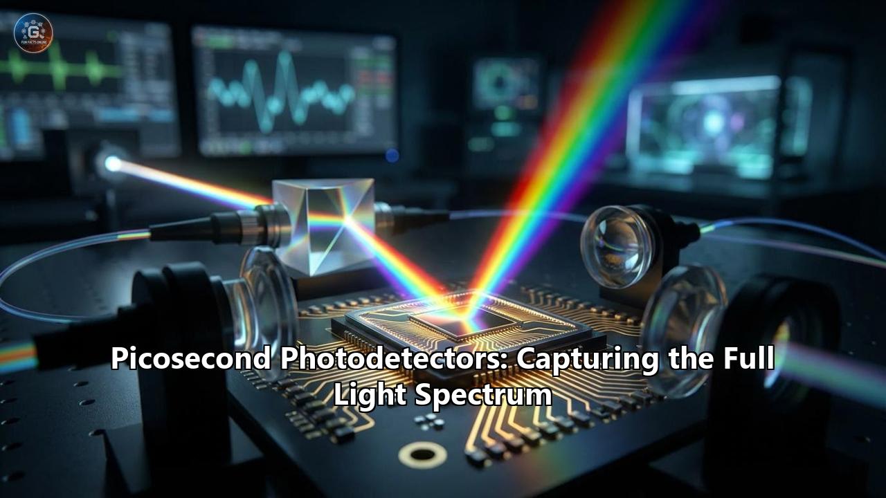
Welcome to the world of picosecond photodetectors.
A picosecond is one-trillionth of a second ($10^{-12}$ seconds). To put this into perspective, there are as many picoseconds in a single second as there are seconds in 31,700 years. In one picosecond, light—the fastest entity in the universe—travels a mere 0.3 millimeters. When we build devices capable of resolving light at this temporal scale, we are no longer just taking pictures; we are mapping the fundamental fabric of spacetime, watching chemical bonds break and form, tracking subatomic particles as they ghost through water, and capturing data encoded in light faster than the blink of an eye.
This is not a theoretical dream. It is an ongoing technological revolution. Through a convergence of high-energy physics, advanced materials science, and nanotechnology, picosecond photodetectors are pushing the boundaries of what is observable. From Large-Area Picosecond Photodetectors (LAPPDs) tracking neutrinos in deep underground tanks to atom-thick graphene photodetectors capturing broadband light at ultrafast speeds, humanity is learning to capture the full light spectrum with unprecedented precision.
In this comprehensive exploration, we will dissect the physics, the materials, the architectures, and the world-altering applications of picosecond photodetectors. We will uncover how capturing the full light spectrum at ultrafast speeds is redefining telecommunications, medical imaging, quantum computing, and our understanding of the cosmos.
The Anatomy of Time and Light
To understand the magnitude of picosecond photodetection, we must first understand the relationship between light, matter, and time.
When a photon strikes a material, its energy is transferred to an electron. In a semiconductor, this energy excites the electron across a "bandgap" from the valence band to the conduction band, creating an electron-hole pair. This process is the foundation of the photoelectric effect. Once liberated, these charge carriers must be swept away by an electric field to create a measurable electrical current.
However, detecting this event quickly is a monumental engineering challenge. Three primary factors limit the speed of a traditional photodetector:
- Transit Time: The time it takes for the electrons and holes to travel through the material to the electrical contacts.
- RC Time Constant: The inherent capacitance (C) and resistance (R) of the device and its readout electronics, which act like a sluggish filter, smearing the sharp electrical pulse into a broad wave.
- Carrier Recombination: If the carriers are not collected fast enough, they will recombine and emit energy as heat or light, destroying the signal.
To achieve picosecond resolution, a photodetector must have an impossibly thin active region (to minimize transit time) coupled with exceptionally low capacitance (to minimize the RC delay), all while absorbing enough photons to generate a discernible signal.
Furthermore, traditional photodetectors are "colorblind" outside their specific bandgap. A silicon photodiode is excellent for visible light and near-infrared (up to about 1,100 nanometers), but it is entirely blind to short-wave infrared (SWIR) or mid-infrared light. Conversely, Indium Gallium Arsenide (InGaAs) is the king of telecommunications wavelengths (1,300 to 1,550 nm) but performs poorly in the visible and ultraviolet ranges. Capturing the "full light spectrum" requires either a mosaic of different materials or the implementation of revolutionary, broadband quantum materials.
Architectures of Ultrafast Photodetection
The quest for picosecond timing has led to several radically different device architectures, each with its own strengths and limitations.
1. PIN Photodiodes
The most common ultrafast detectors are PIN photodiodes. They consist of a P-type semiconductor, an intrinsic (undoped) layer, and an N-type semiconductor. The intrinsic layer creates a wide depletion region where photons are absorbed. By applying a reverse bias voltage, a strong electric field is generated across this region. When a photon creates an electron-hole pair, the electric field violently sweeps them to the opposite contacts. By making the intrinsic layer incredibly thin (often just a few micrometers or less), engineers can drive the transit time down to the picosecond range. However, a thinner intrinsic layer absorbs fewer photons, leading to a tradeoff between speed and "quantum efficiency" (the percentage of incoming photons that generate an electron).
2. Avalanche Photodiodes (APDs) and Single-Photon Avalanche Diodes (SPADs)
When detecting faint light—sometimes just a single photon—a standard PIN diode isn't enough; the electrical signal is drowned out by the thermal noise of the circuit. Avalanche Photodiodes solve this by using an internal multiplication mechanism. A high reverse bias voltage accelerates the initial photo-generated electron to such a high velocity that when it collides with the crystal lattice, it knocks more electrons loose. These new electrons are also accelerated, creating an "avalanche" of charge.
When the voltage is pushed beyond the material's breakdown threshold, the device operates in the "Geiger mode." This is a SPAD. A single photon triggers a massive, self-sustaining avalanche, resulting in a macroscopic current pulse. Because the avalanche process builds up incredibly fast, SPADs can achieve timing resolutions in the range of tens of picoseconds. They are the beating heart of modern LiDAR systems and quantum cryptography networks.
3. Microchannel Plate Photomultiplier Tubes (MCP-PMTs)
For large-scale physics experiments and advanced imaging, solid-state detectors often fall short in providing large-area coverage. Here, Microchannel Plate Photomultiplier Tubes (MCP-PMTs) reign supreme.
An MCP-PMT operates in a vacuum. A photon strikes a photocathode (often a bi-alkali material), causing it to emit an electron into the vacuum via the photoelectric effect. This electron is accelerated toward a microchannel plate—a thin disk of glass honeycombed with millions of microscopic tubes (pores) that are typically 10 to 20 micrometers in diameter.
A high voltage is applied across the plate. When the electron enters a pore and strikes the wall, it knocks loose secondary electrons. These electrons are accelerated further down the pore, striking the walls again and again, multiplying exponentially. A single photon can result in a cascade of ten million electrons hitting the anode at the bottom of the tube. Because the electrons travel very short distances inside these microscopic pores, the signal arrives with astonishingly low "time jitter" (the variance in arrival time), frequently below 50 picoseconds.
The LAPPD Revolution: Scaling the Microscopic
For decades, MCP-PMTs were the gold standard for ultrafast single-photon detection, but they had a fatal flaw: they were small, fragile, and excruciatingly expensive to manufacture. Traditional MCPs were made by drawing, bundling, and etching heavily doped lead-silicate glass—a process closer to artisanal glassblowing than modern semiconductor manufacturing. If you wanted to cover a large area—say, the walls of a massive neutrino detector—you would need thousands of these tubes, costing hundreds of millions of dollars.
Enter the Large-Area Picosecond Photodetector (LAPPD) project.
Spearheaded by high-energy physicists and funded by the U.S. Department of Energy, a multi-institutional collaboration—including Fermilab, Argonne National Laboratory, the University of Chicago, and commercial partner Incom Inc.—set out to democratize picosecond timing.
The LAPPD is a flat-panel MCP-PMT boasting a massive active area of 200 mm x 200 mm (400 square centimeters)—the largest and fastest detector of its kind. To achieve this, the collaboration threw out the traditional manufacturing rulebook. Instead of lead-silicate glass, they used cheap, widely available borosilicate float glass to create glass capillary arrays (GCAs).
But borosilicate glass cannot multiply electrons. To solve this, the researchers turned to Atomic Layer Deposition (ALD). ALD is a process that deposits materials one atomic layer at a time. The inside of millions of microscopic pores in the borosilicate glass were coated with an ultra-thin resistive layer, followed by an emissive layer capable of yielding high numbers of secondary electrons.
The result is a hermetically sealed, all-glass detector that achieves a spatial resolution of about 1 millimeter and a timing resolution of roughly 50 picoseconds for a single photon. At these speeds, the LAPPD can measure not just where a photon hit, but when it hit, effectively creating a 3D reconstruction of light in real-time. When tested with sub-picosecond pulsed Ti:Sapphire lasers, LAPPDs showcased electron gains exceeding $10^7$ and incredibly low dark noise rates.
The first major deployment of LAPPDs is in the ANNIE (Accelerator Neutrino Neutron Interaction Experiment) detector at Fermilab. Neutrinos are ghostly, near-massless particles that rarely interact with matter. When they do interact with the water inside the ANNIE tank, they produce charged particles traveling faster than the speed of light in water. This emits a sonic boom of light known as Cherenkov radiation. By capturing the precise arrival times and locations of these faint blue Cherenkov photons on the walls of the tank, the LAPPDs allow physicists to mathematically rewind time, reconstructing the exact 3D tracks, energies, and origins of the particles with unprecedented clarity.
Capturing the Full Spectrum: The Quest for Broadband Materials
While devices like LAPPDs excel at detecting single photons of visible and ultraviolet light (thanks to their bi-alkali photocathodes), they cannot see the infrared or terahertz spectrum. Capturing the full light spectrum—from high-energy UV down to low-energy mid-infrared—requires a radical departure from traditional materials.
1. The Limits of Silicon and InGaAs
Silicon dominates the visible spectrum, and InGaAs dominates the near-infrared. However, combining them is difficult due to "lattice mismatch." If you try to grow InGaAs crystals on a silicon wafer, the differing atomic spacing causes the crystals to fracture and fail. Furthermore, neither material can detect mid-infrared light efficiently. To see further into the infrared, engineers have historically relied on exotic and toxic materials like Mercury Cadmium Telluride (HgCdTe), which require cryogenic cooling to prevent thermal noise from swamping the sensitive signals.
2. The Graphene Miracle
In the search for a true broadband, room-temperature, ultrafast photodetector, scientists found their holy grail in a single layer of carbon atoms: graphene.
Graphene is a two-dimensional lattice of carbon atoms arranged in a hexagonal honeycomb structure. From an electronic standpoint, it is a "zero-bandgap" semiconductor. Because it has no bandgap, it can absorb photons of virtually any energy—from ultraviolet light all the way down to the far-infrared and terahertz frequencies. It literally absorbs across the entire optical spectrum.
However, because graphene is only one atom thick, it only absorbs about 2.3% of the light that passes through it. For a long time, this weak absorption limited its use in commercial photodetectors. Furthermore, because it has no bandgap, the excited electrons and holes recombine incredibly fast—often within femtoseconds—before they can be extracted as an electrical current.
But what was initially seen as a weakness (ultrafast recombination) was weaponized into a strength by researchers at the Institute of Photonic Sciences (ICFO), MIT, and the European Graphene Flagship. They realized that the ultrafast carrier dynamics in graphene could enable the fastest photodetectors ever built.
In a groundbreaking demonstration, scientists developed a graphene-based photodetector that converts light into electricity in under 50 femtoseconds ($50 \times 10^{-15}$ seconds). This was facilitated by graphene's nonlinear photo-thermoelectric response. When a photon hits graphene, rather than just creating a simple electron-hole pair, the energy rapidly heats up a "puddle" of surrounding electrons. Because graphene conducts heat and electricity so well, these "hot carriers" can be swept out of the material at staggering speeds.
To solve the problem of low absorption (the 2.3% issue), engineers at institutions like Stanford University integrated graphene directly onto silicon photonic waveguides. Instead of shining light perpendicular to the graphene (where it quickly passes through), the light is channeled horizontally through a silicon waveguide. The graphene sits on top of this optical fiber-like channel. As the light travels down the waveguide, its evanescent field interacts continuously with the graphene over a long distance, boosting absorption close to 100%.
This waveguide-integrated graphene photodetector simultaneously exhibited high responsivity, a nearly uniform broad spectral bandwidth (spanning telecommunications wavelengths of 1450 to 1590 nm and beyond), and operation speeds exceeding 20 GHz without even requiring an external bias voltage (zero-bias operation). Graphene's unique property of "carrier multiplication"—where one high-energy photon excites multiple electrons—provides inherent gain to the system, much like an avalanche photodiode, but without the extreme voltages or noise.
Through interfacial gating effects—such as placing graphene on lightly doped silicon substrates with built-in electric fields—engineers have successfully bridged the gap between ultrafast response and ultra-sensitivity, creating devices capable of seeing from the visible to the near-IR with response times pushed to nanosecond and picosecond domains.
3. Perovskites: The Rising Stars
While graphene reigns supreme for ultra-broadband and ultrafast communications, organometal halide perovskites are emerging as the champions of high-efficiency, cost-effective detection. Perovskites are materials that share the crystal structure of calcium titanate. They have taken the solar cell industry by storm, but their exceptional optoelectronic properties make them brilliant photodetectors.
Perovskites have high absorption coefficients, meaning a very thin layer can absorb a massive amount of light. Crucially, their bandgap is highly tunable. By slightly altering their chemical composition (e.g., swapping out iodine for bromine or chlorine), engineers can tune the perovskite to absorb specific wavelengths across the entire visible and near-infrared spectrum.
Recent advancements have allowed researchers to fabricate perovskite picosecond photodetectors by combining them with ultrafast charge-transport layers. When a laser pulse strikes the perovskite, the highly mobile charge carriers are instantly injected into adjacent transport layers (like carbon nanotubes or specialized polymers). This mitigates the recombination issue and allows for response times in the picosecond regime, making them ideal for next-generation, flexible, and printable imaging arrays.
4. Plasmonic Metamaterials
To push the limits of light capture even further, scientists are engineering the very geometry of the detectors using plasmonic metamaterials. By etching nanoscale gold or silver structures (like tiny antennas) onto the surface of a photodetector, they can manipulate light at scales smaller than its own wavelength.
These optical antennas capture incoming light from a broad spectrum and concentrate it into incredibly intense "hotspots" exactly where the semiconductor or graphene absorbs it. This localized surface plasmon resonance drastically enhances the quantum efficiency of the detector while allowing the active absorbing volume to remain incredibly small. The smaller the volume, the lower the capacitance; the lower the capacitance, the faster the speed. Plasmonic-enhanced photodetectors routinely operate in the picosecond and femtosecond regimes, bridging the gap between optics and electronics.
The Readout Challenge: Measuring the Unmeasurable
Building a detector that responds in 50 picoseconds is only half the battle. You also need electronics capable of recording a signal that fast. If your detector generates a perfect 50-picosecond spike, but your oscilloscope or readout chip has a resolution of 1 nanosecond, the temporal precision is lost.
The readout of picosecond photodetectors requires Application-Specific Integrated Circuits (ASICs) featuring highly advanced Time-to-Digital Converters (TDCs). A TDC is essentially a digital stopwatch that measures the arrival time of an electrical pulse.
For large arrays like the LAPPD, which generate massive amounts of data across multiple channels, electronics must be both fast and scalable. In high-energy physics experiments, specialized ASICs like the PETsys TOFPET 2 and the FastIC have been tested extensively. The TOFPET 2 ASIC, for instance, provides dual-branch analogue interpolation TDCs with a time binning of just 30 picoseconds. The FastIC ASIC, built on 65 nm CMOS technology, achieves electronic time jitter of roughly 25 picoseconds.
These chips do not just record time; they also record the "Time-over-Threshold" (ToT), which allows them to estimate the amplitude (charge) of the incoming signal. By combining the exact arrival time, the spatial coordinates from the detector pad (which can be 1 millimeter or smaller), and the charge of the pulse, engineers can perfectly reconstruct the photonic event.
Transformative Applications: What Can We Do With a Picosecond?
The ability to detect broad-spectrum light at picosecond resolution is not just an academic exercise. It is a foundational technology that is quietly rewriting the rules of numerous global industries.
1. Next-Generation Optical Communications and Datacenters
The internet is built on light. Every email, streaming video, and financial transaction travels across the globe as pulses of infrared light bouncing through fiber optic cables. In modern datacenters, the sheer volume of data is causing an energy and bandwidth bottleneck.
To transmit more data, we must pack the light pulses closer together. If a photodetector has a slow response time, the tail end of one light pulse will bleed into the beginning of the next, causing "Inter-Symbol Interference" (ISI). A picosecond photodetector can clearly resolve light pulses separated by mere trillionths of a second. Graphene-based photodetectors, with their 50-femtosecond intrinsic response times and uniform spectral absorption across telecom wavelengths, are poised to enable operation rates exceeding 100 Gigabits per second per single channel, moving toward terahertz bandwidths. By integrating these ultrafast detectors directly onto silicon photonic chips, we can drastically reduce the power consumption and latency of global communication networks.
2. Time-of-Flight Positron Emission Tomography (TOF-PET)
In the realm of medical imaging, picosecond timing is a matter of life and death. Positron Emission Tomography (PET) is a technique used to detect cancer. A patient is injected with a mildly radioactive sugar tracer that accumulates in tumors. When the radioactive isotope decays, it emits a positron, which immediately collides with an electron. This annihilation event produces two gamma-ray photons that shoot out in exactly opposite directions.
The PET scanner consists of a ring of scintillating crystals that convert gamma rays into flashes of visible light, which are then detected by photodetectors. If the detector captures both photons simultaneously, the computer knows the tumor lies somewhere on the line between the two detectors.
However, if the photodetectors have a timing resolution of 10 picoseconds, the system can measure the exact time difference between the arrival of the two photons. Because light travels at a known speed (300 picoseconds per millimeter), a 10-picosecond timing difference allows doctors to pinpoint the location of the tumor along that line to within a few millimeters. This is known as Time-of-Flight PET (TOF-PET). It dramatically improves image contrast, reduces radiation doses, and allows for the detection of millimeter-sized micro-tumors that traditional PET scans would miss entirely. LAPPDs and advanced SiPMs (Silicon Photomultipliers) are directly driving this revolution in oncology.
3. LiDAR and Autonomous Vehicles
Light Detection and Ranging (LiDAR) is the "vision" system of autonomous vehicles. A laser fires a pulse of light, which bounces off a pedestrian or another car and returns to the sensor. By measuring the time it took for the light to return, the car calculates the distance.
A car driving at 70 mph needs to make split-second decisions. Furthermore, the environment is chaotic—sunlight, headlights, and rain all create optical noise. Broadband picosecond photodetectors (particularly those operating in the SWIR spectrum, like 1550 nm, which is safe for human eyes and penetrates fog better than visible light) allow for hyper-accurate, millimeter-level 3D spatial resolution. The ultrafast timing allows the sensor to differentiate between a true laser return and ambient light, ensuring the safety of autonomous navigation.
4. Fluorescence Lifetime Imaging Microscopy (FLIM)
In biology, understanding the chemical environment inside a living cell is incredibly difficult. Fluorescence Lifetime Imaging Microscopy (FLIM) solves this by using fluorescent dyes that attach to specific molecules.
When excited by a laser, these dyes glow. But it is not the brightness of the glow that matters; it is the lifetime of the glow. Depending on the pH, oxygen levels, or calcium concentration in the cell, the fluorescence will fade away in a matter of hundreds of picoseconds to nanoseconds. By using picosecond photodetectors to measure exactly how long the glow lasts, biologists can map the biochemical environment inside living, breathing cells in real-time, aiding in the discovery of new pharmaceuticals and understanding neurodegenerative diseases.
5. Quantum Cryptography and Computing
The future of cybersecurity relies on quantum mechanics. Quantum Key Distribution (QKD) uses individual photons to generate unbreakable encryption keys. If an eavesdropper tries to intercept the photon, the laws of quantum mechanics dictate that the state of the photon will change, instantly alerting the communicators to the breach.
This requires detectors that are not only capable of single-photon sensitivity but also exact timing to filter out "dark counts" (false signals generated by thermal noise) and ambient stray light. Ultrafast, broadband photodetectors are critical nodes in the developing "quantum internet," allowing for secure communications over immense distances.
6. Astrophysics and Deep Space Exploration
When astronomers look at the farthest edges of the observable universe, they are dealing with incredibly faint light that has been stretched (redshifted) into the infrared by the expansion of space. Capturing this full spectrum of light requires massive telescope arrays equipped with ultra-sensitive, broadband photodetectors. Furthermore, the burgeoning field of deep-space optical communication—where NASA transmits high-def video from Mars to Earth via lasers instead of radio waves—relies exclusively on the ability of ground-based telescopes to detect picosecond laser pulses against the blinding background of the sunlit sky.
Challenges on the Horizon
Despite the awe-inspiring capabilities of picosecond photodetectors, significant hurdles remain before they reach ubiquitous commercialization.
- Dark Current and Thermal Noise: Especially in broadband materials like graphene and narrow-bandgap infrared detectors, thermal energy at room temperature can spontaneously excite electrons, creating a "dark current" that mimics a true light signal. While graphene's unique properties mitigate some of this, achieving true single-photon sensitivity in the mid-infrared without cryogenic cooling remains a massive physics challenge.
- Integration with CMOS: Silicon-based computer chips (CMOS) are incredibly cheap and scalable. However, integrating exotic materials like perovskites, InGaAs, or even complex microchannel plates with silicon electronics is difficult. Differences in thermal expansion, lattice matching, and chemical compatibility require complex manufacturing workarounds. The success of waveguide-integrated graphene is a major leap forward, but large-scale foundry production is still in its infancy.
- Data Deluge: An array of picosecond photodetectors generating thousands of frames per second yields an astronomical amount of data. Processing this data requires immense computational power. We are reaching a point where the bottleneck is no longer the detector itself, but the computer's ability to ingest and process the picosecond timestamps in real-time.
The Future: Into the Femtosecond Realm
As we push deeper into the 21st century, the lines between electronics and optics will continue to blur. The research spearheaded by the Graphene Flagship and others has already proven that converting light to electricity in under 50 femtoseconds is possible.
The next frontier is "on-chip AI photonics." Rather than sending the massive stream of picosecond data to a traditional CPU, researchers are developing neural networks built directly into the optical chip. By using the interference patterns of light itself to perform matrix multiplications, these chips will analyze the ultrafast signals the instant they are detected, enabling true zero-latency decision-making for autonomous vehicles and robotic surgery.
Furthermore, the expansion of meta-materials will allow us to design "smart pixels." Imagine a single, flat pixel on a camera sensor that can simultaneously detect the intensity of light, its exact wavelength (color), its polarization, and its arrival time down to the picosecond. A camera built from such sensors would not just take a picture; it would capture a complete holographic and biochemical snapshot of reality.
Conclusion
The development of picosecond photodetectors represents a monumental triumph of human ingenuity. We have taken the most elusive, intangible element of our universe—light—and built microscopic traps capable of catching it in mid-flight, a trillionth of a second at a time.
From the cavernous, water-filled tanks of neutrino observatories where LAPPDs track the fundamental building blocks of the universe, to the ultra-thin, waveguide-integrated graphene sheets powering the next generation of global internet, the ability to capture the full light spectrum at ultrafast speeds is transforming our relationship with reality.
We are moving from a society that merely observes the world to one that mathematically dissects it in real-time. Time-of-flight medical imaging will find diseases before they take hold. LiDAR systems will map our environments with flawless precision. And optical telecommunications will weave a web of data so vast and fast that the concept of "buffering" will become an artifact of history.
We have finally cured our evolutionary blindness. By capturing the full light spectrum at the speed of picoseconds, we are no longer just looking at the universe; we are seeing it exactly as it is.
Reference:
- https://annie.fnal.gov/lappds/
- https://www.osti.gov/servlets/purl/1564252
- https://pubmed.ncbi.nlm.nih.gov/19893532/
- https://graphene-flagship.eu/materials/news/ultrafast-photodetectors-with-graphene
- https://agenda.hep.wisc.edu/event/1391/contributions/6984/attachments/1704/1918/lyashenko_CPAD19_presentation_final.pdf
- https://incomusa.com/lappd/
- https://indico.cern.ch/event/192695/contributions/353328/contribution.pdf
- https://web.stanford.edu/group/heinz/publications/Pub212.pdf
- https://www.graphene-info.com/scientists-develop-graphene-based-ultrafast-photodetector
- https://validate.perfdrive.com/?ssa=72fd52c0-e113-e35b-d21a-598e39da277f&ssb=92947208491&ssc=https%3A%2F%2Fopg.optica.org&ssi=0de8ae6a-d3hy-0c6e-4beb-f2a20220876f&ssk=botmanager_support@radware.com&ssm=29223423022999275133024173664615&ssn=4b2a2160f129ffa5f7a073529a1c45c1894064f1f592-ccb3-5b65-f7dfb6&sso=df17965-f930-6602a4bd20d7395cc98ecebb3743cc64d4695b323afaa3f6&ssp=09864389841774035920177400523553991&ssq=41192528209335878899482092443656199644735&ssr=MTgwLjE4OC4xNzQuMjg=&sst=python-requests%2F2.32.3&ssv=&ssw=
- https://indico.global/event/1725/contributions/30475/attachments/15542/24773/PSD13_poster_krizan.pdf