The history of human technological advancement is often chronicled by the materials that defined the era: the Stone Age, the Bronze Age, the Iron Age, and for the last half-century, the Silicon Age. We are now standing on the precipice of a new epoch. It is a transition not merely to a new material, but to the ultimate material. We are entering the Diamond Age.
For decades, diamond has been the "crown jewel" of semiconductors—a material so theoretically perfect that it was often dismissed as a physicist's daydream, unobtainable for practical mass production. Its thermal conductivity is five times that of copper; its breakdown voltage is thirty times that of silicon; and its electron mobility is unsurpassed. Yet, it remained a gemstone rather than a circuit, locked away by the immense difficulty of processing the hardest natural substance on Earth.
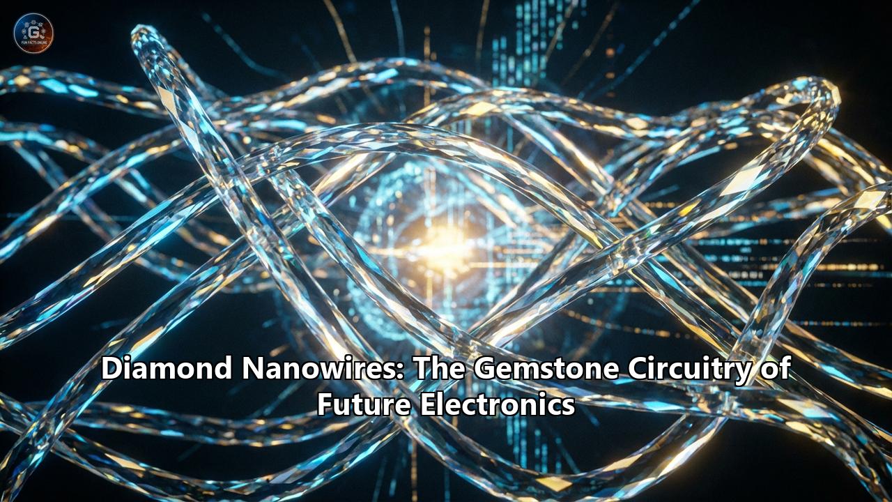
That narrative has changed. A convergence of breakthroughs in nanotechnology, quantum physics, and chemical vapor deposition (CVD) has given rise to a new class of materials: Diamond Nanowires (DNWs). These are not merely small diamonds. They are one-dimensional crystalline structures that bend the rules of classical physics, allowing for the creation of "gemstone circuitry" that operates at speeds, temperatures, and efficiencies previously thought impossible.
This is the comprehensive story of diamond nanowires—how they are made, why they are destined to replace silicon in critical applications, and how they will form the backbone of the next century’s electronics, from quantum computers to interstellar spacecraft.
Part I: The Silicon Ceiling and the Diamond Promise
To understand the inevitability of diamond electronics, one must first understand the impending failure of silicon. For sixty years, Moore’s Law has been the heartbeat of the modern world, predicting the doubling of transistors on a chip every two years. But silicon is hitting a wall—literally and thermally. As transistors shrink to the atomic scale, silicon begins to leak current (quantum tunneling) and overheat. The heat generated by modern high-performance chips is becoming unmanageable, requiring massive cooling infrastructure that consumes gigawatts of energy globally.
Silicon is a "narrow bandgap" semiconductor (1.1 eV). This means it takes relatively little energy to knock an electron loose and create a current. While this makes it easy to work with, it also means that at high voltages or temperatures, silicon becomes conductive when it shouldn’t, leading to failure.
Enter the Wide Bandgap TitanDiamond is an "ultra-wide bandgap" semiconductor (5.47 eV). This massive energy gap means diamond acts as a perfect insulator until a specific, high-energy threshold is met, at which point it becomes a hyper-efficient conductor. This property alone allows diamond devices to operate at voltages that would instantly vaporize silicon.
But the "Gemstone Circuitry" goes beyond mere power handling.
- Thermal Superconductivity: Diamond is the best thermal conductor known to man (2200 W/mK). A diamond chip doesn't just tolerate heat; it actively sucks it away from the active circuits. This eliminates the need for bulky fans and heatsinks, allowing for denser, faster processors.
- Carrier Mobility: Electrons and "holes" (the absence of electrons) move through diamond with incredible speed. In fact, diamond has the highest known saturation velocity for carriers, meaning that at high frequencies (terahertz range), diamond transistors can switch faster than any other material.
- Chemical Immortality: Diamond is chemically inert. It can operate in corrosive environments, inside the human body, or in the radiation-soaked vacuum of space without degrading.
Part II: The Nanowire Revolution
If diamond is so great, why hasn't it replaced silicon yet? The answer lies in the difficulty of "doping" (adding impurities to create conductivity) and the brittleness of bulk diamond. This is where the nanowire geometry changes everything.
1. The Strain Engineering MiracleBulk diamond is rigid. If you try to stretch it, it shatters. However, when diamond is synthesized as a nanowire—a strand only tens of nanometers thick—it gains a surprising property: elasticity. Diamond nanowires can be bent and strained up to 9% without breaking.
This "elastic strain engineering" allows physicists to tune the electronic properties of the diamond. By stretching the nanowire, they can alter its bandgap, effectively turning it from an insulator into a conductor or even a superconductor, without chemical doping. This is a capability unique to the nanoscale, turning the diamond's rigidity into a tunable instrument.
2. The Defect-Free ChannelGrowing large, single-crystal diamond wafers is notoriously difficult and expensive. Defects (cracks, impurities) in the crystal lattice kill performance. Nanowires, however, can be grown "bottom-up" or etched "top-down" with near-perfect crystallinity. Because they are so small, they can effectively "push" defects out to the surface, leaving a pristine core for electrons to travel through. This results in ballistic transport, where electrons fly through the wire without hitting any obstacles, minimizing heat and maximizing speed.
3. The Surface-to-Volume RatioIn a nanowire, a huge percentage of the atoms are on the surface. This makes diamond nanowires incredibly sensitive sensors. By attaching biological molecules to the surface of a diamond nanowire, researchers can detect single viruses or protein markers. The chemical inertness of diamond means these sensors are biocompatible, paving the way for "smart implants" that can monitor blood chemistry in real-time without being rejected by the body.
Part III: The "Holy Grail" – N-Type Doping and the New Circuitry
For a material to function as a transistor (the on/off switch of computing), you need two types of semiconductors: p-type (positive charge carriers) and n-type (negative charge carriers).
- P-type diamond is relatively easy to make by adding Boron. The Boron atoms fit the diamond lattice well and provide "holes" for conduction.
- N-type diamond has been the nightmare of materials science for 40 years. The standard dopants (like Phosphorus or Nitrogen) are physically larger than carbon atoms. Forcing them into the tight diamond lattice causes distortions and cracks. Furthermore, the electrons they provide are "deep," meaning they are stuck tightly to the atom and don't want to move at room temperature.
In late 2023 and throughout 2024, research teams in Japan (notably NIMS) and Europe cracked the code. Using a technique called "step-flow growth" on (001)-oriented diamond substrates, they managed to incorporate Phosphorus into the lattice with atomic precision, minimizing defects.
This led to the creation of the world’s first n-channel diamond MOSFET (Metal-Oxide-Semiconductor Field-Effect Transistor) that operates efficiently at high temperatures.
- Why this matters: With both p-channel and n-channel diamond transistors now available, engineers can build CMOS (Complementary Metal-Oxide-Semiconductor) logic—the fundamental architecture of all modern processors.
- The Result: We can now build "all-diamond" logic gates (NAND, NOR, Inverters) that function at 300°C (572°F) and withstand thousands of volts. This is the birth of true Gemstone Circuitry.
Part IV: Quantum Computing’s Golden Wire
While diamond electronics will revolutionize power and speed, their most profound impact may be in Quantum Computing.
Classical computers use bits (0 or 1). Quantum computers use qubits, which can be both 0 and 1 simultaneously. The problem is that qubits are notoriously fragile; the slightest vibration or temperature fluctuation causes them to "decohere" and lose data. Most quantum computers today (like those from Google or IBM) require massive dilution refrigerators to keep the chips near absolute zero.
The Nitrogen-Vacancy (NV) CenterDiamond has a magic trick: the Nitrogen-Vacancy center. This is a specific defect where a Nitrogen atom sits next to a missing carbon atom in the lattice. This NV center acts as a natural qubit. It has an electron spin that can be controlled with light and microwaves, and remarkably, it works at room temperature.
The Nanowire WaveguideThe challenge has been getting the information out of the diamond. The high refractive index of diamond means light tends to get trapped inside (total internal reflection)—this is why cut diamonds sparkle, but it’s a nightmare for data transmission.
Diamond nanowires solve this. By embedding an NV center inside a nanowire, the wire acts as a waveguide, funneling the emitted photons (quantum data) directly into a fiber optic cable with high efficiency.
- Recent Advance (2025): Researchers at the Hebrew University of Jerusalem and Humboldt University developed "hybrid nanoantennas" around diamond nanostructures, capturing 80% of the emitted photons.
- The Vision: A quantum computer made of millions of diamond nanowires, each holding a stable qubit, operating at room temperature on a desktop. This would democratize quantum power, moving it from supercooled labs to data centers and even vehicles.
Part V: Synthesis – forging the Future
How do we manufacture these gemstone circuits? We are long past the days of mining diamonds from the earth. The future is grown in the lab.
1. CVD (Chemical Vapor Deposition)This is the workhorse method. A substrate is placed in a vacuum chamber filled with methane and hydrogen gas. Microwaves turn the gas into a plasma, breaking the carbon bonds. The carbon rains down and crystallizes as diamond. By pulsing the gas flow or using metal catalysts (like gold nanoparticles), wires can be grown upwards like grass.
2. The Liquid Metal Breakthrough (2024)A team from the Institute for Basic Science (IBS) in Korea stunned the world by growing diamond in liquid metal (gallium-nickel-iron-silicon alloy) at just 1 atmosphere of pressure. This effectively allows diamond to be "painted" onto substrates, drastically lowering the cost and complexity compared to high-pressure methods.
3. Electron Beam Writing (2025)Researchers at the University of Tokyo discovered that electron beams can transform organic molecules (adamantane) directly into diamond nanostructures without heat or pressure. This allows for "direct write" lithography—drawing diamond circuits directly onto a chip with atomic precision.
Part VI: Applications – The World After Silicon
1. The Electric Vehicle (EV) RevolutionCurrent EVs are limited by their power inverters (which convert battery DC to motor AC). Silicon inverters are heavy, inefficient, and require water cooling.
- The Diamond Solution: Diamond inverters are 6x smaller and lighter. They can sit directly on the motor (handling the heat) and switch energy with 99% efficiency. This could extend EV range by 15-20% without changing the battery.
5G is here, but 6G will require frequencies in the Terahertz range. Silicon cannot switch fast enough. Gallium Nitride (GaN) struggles with the heat. Diamond nanowire transistors are the only known technology capable of handling the high power and high frequency required for 6G satellites and base stations.
3. Deep Space & Nuclear ExplorationElectronics on missions to Jupiter or inside nuclear reactors must be shielded with pounds of lead to survive radiation. Diamond is radiation-hard. A diamond nanowire computer could sit unshielded in the heart of a reactor or on the surface of Europa, gathering data where no silicon chip could survive.
4. Bionic InterfacesBecause carbon is the basis of life, diamond is not rejected by the human body. Diamond nanowire retinal implants are being developed to restore sight. The wires are small enough to stimulate individual neurons, and durable enough to last a lifetime without corroding.
Conclusion: The Age of Carbon
We are witnessing the maturity of a technology that was once science fiction. The "Gemstone Circuitry" of diamond nanowires is no longer just a theoretical possibility; it is an engineering reality being refined in cleanrooms across the globe.
The transition will be gradual. First, diamond will appear in high-end power inverters and RF amplifiers. Then, in quantum sensors and medical implants. Finally, as manufacturing costs plummet, we may see the first all-diamond processors—chips that run at 100 GHz, never get hot, and last forever.
From the black soot of carbon, we are weaving the crystalline threads of the future. The Diamond Age is here, and it is brilliant.
Reference:
- https://www.livescience.com/technology/electronics/new-diamond-transistor-is-a-world-1st-paving-the-way-for-high-speed-computing-at-the-highest-temperatures
- https://www.sciencedaily.com/releases/2024/03/240321155340.htm
- https://theevreport.com/diamond-based-inverter-unveiled
- http://lab.semi.ac.cn/download/0.7407707867682094.pdf