For decades, the trajectory of display technology has been defined by a relentless pursuit of resolution and realism. From the bulky, cathode-ray tube televisions of the 20th century to the sleek, self-illuminating organic light-emitting diode (OLED) screens that grace our living rooms today, the goal has always been to recreate the visual fidelity of the natural world. Yet, as we push into an era dominated by augmented reality (AR), virtual reality (VR), and advanced micro-displays, the traditional metrics of high definition—measured in a few hundred pixels per inch (PPI)—have suddenly become profoundly inadequate. When a screen is situated mere millimeters from the human eye, the illusion of reality shatters; individual pixels become visible, creating a grid-like distraction known as the "screen door effect."
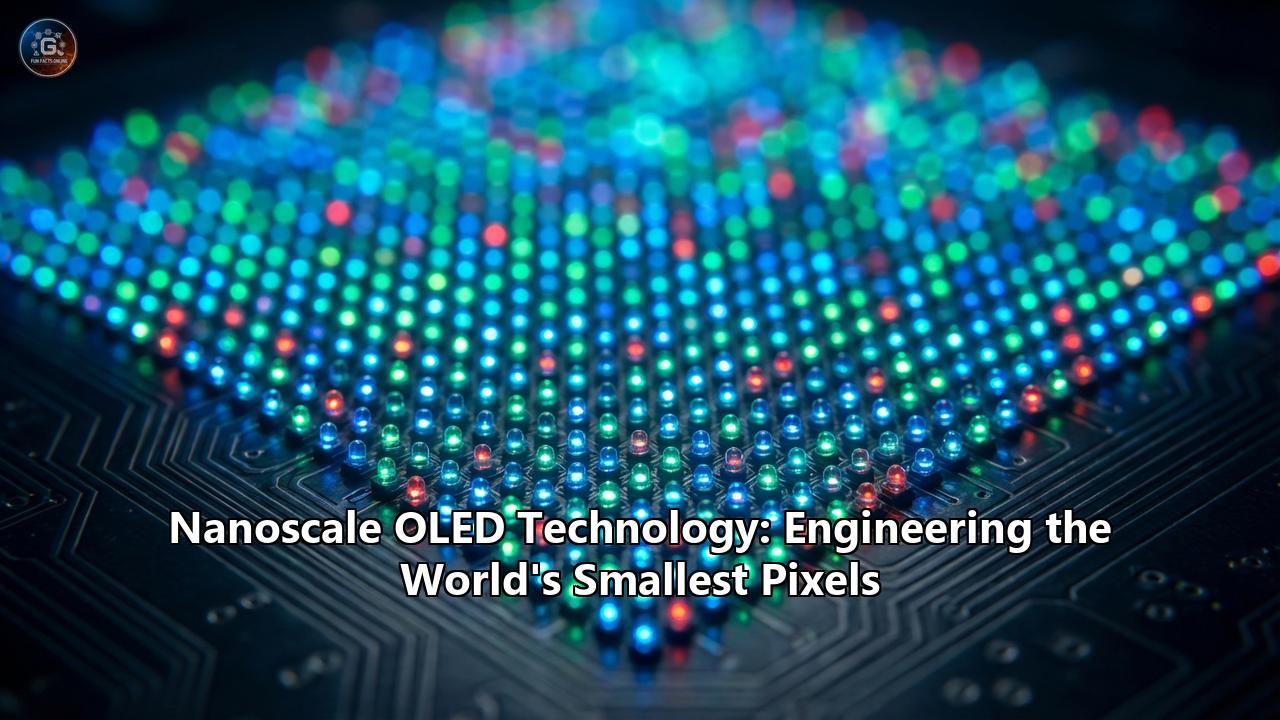
To overcome this, the display industry has embarked on one of the most ambitious engineering challenges in modern applied physics: scaling OLED technology down to the nanoscale. We are no longer talking about shrinking pixels by fractions of a millimeter. Today’s researchers and materials scientists are engineering individual light-emitting diodes that are smaller than a single bacterium, and in some cases, smaller than the wavelength of the light they emit. This monumental shift is pushing the boundaries of quantum mechanics, nanophotonics, and materials science, giving birth to displays that pack up to 10,000—and even 100,000—pixels into a single inch.
The transition from microscale to nanoscale OLEDs is not simply a matter of making things smaller. It requires entirely new architectures, novel materials, and a fundamental rethinking of how light is generated, directed, and extracted.
The Quantum Hurdles of Shrinking Light
To appreciate the magnitude of engineering a nanoscale OLED, one must first understand how a traditional OLED functions. At its core, an OLED is a sandwich of ultra-thin organic carbon-based films situated between two electrical conductors (an anode and a cathode). When an electrical current is applied, electrons and "holes" (the absence of an electron) are injected into the organic layers. They meet in an emissive layer, recombining to release energy in the form of photons—light.
In a conventional smartphone or television display, these pixels are relatively massive, typically measuring tens of micrometers across. At this scale, the flow of electricity is uniform, and light escapes the organic materials with relative ease. However, when engineers attempt to shrink this architecture down to the nanometer scale—below the 400 to 700-nanometer wavelengths of visible light—the physics abruptly change.
The primary obstacle is a phenomenon analogous to a lightning rod. At subwavelength scales, the geometry of the electrodes causes severe imbalances in the distribution of electricity. Instead of flowing smoothly across the pixel, the current surges at the sharp edges and corners of the nano-electrodes. This uneven distribution triggers "filamentation," where localized spikes in energy literally burn tiny conductive pathways through the delicate organic material, short-circuiting the pixel and causing immediate device failure.
Furthermore, as pixels get smaller, the "efficiency roll-off" becomes severe. A massive proportion of the generated light ends up trapped inside the device due to internal reflection, bouncing around the substrate rather than traveling outward to the viewer's eye. If you shrink a traditional OLED pixel to less than a micrometer, its brightness plummets, rendering it useless for practical applications. Overcoming these quantum and optical bottlenecks required scientists to look outside the realm of traditional display engineering and venture into the exotic world of metaphotonics.
The Metasurface Miracle: Stealing Secrets from the Sun
The first major breakthrough in the quest for the ultimate nanoscale pixel came from an unexpected collaboration between solar energy researchers at Stanford University and the Samsung Advanced Institute of Technology (SAIT). While attempting to design ultra-thin solar panels that could absorb light more efficiently, Stanford scientists realized that at the nanoscale, light does not behave like a rigid ray; it flows around objects like water.
If nanoscale structures could be used to trap light in a solar panel, the researchers theorized, similar structures could be used in reverse to extract light from an ultra-dense OLED. This lateral thinking led to the invention of the "metaphotonic OLED."
The crucial innovation in this architecture is the replacement of the standard flat electrode with an optical metasurface—a base layer of highly reflective metal etched with billions of nanoscale corrugations. These microscopic pillars and grooves act as an intricate optical antenna array. By precisely altering the height and spacing of these nanostructures, the researchers could manipulate the reflective properties of light, creating localized optical resonances.
In a traditional OLED display, producing distinct colors usually requires side-by-side subpixels (red, green, and blue) or a white light emitter layered beneath color filters. Color filters are inherently inefficient because they work by blocking light; a red filter, for example, absorbs the green and blue wavelengths, wasting a massive amount of the energy generated by the pixel.
The optical metasurface eliminates the need for filters entirely. The Stanford and Samsung team deposited a uniform layer of white organic emitters over the corrugated nanoscale mirrors. Depending on the specific pattern of the metasurface beneath a given pixel, the physical structure itself forces the light to resonate at a specific frequency, extracting pure red, pure green, or pure blue light.
The results were paradigm-shifting. Because the organic layer is uniform across the entire display, manufacturing becomes significantly simpler and highly scalable using nanoimprint lithography. More importantly, these metasurface pixels boast a twofold increase in luminescence efficiency and vastly superior color purity compared to standard color-filtered OLEDs. This architecture successfully demonstrated pixel densities exceeding 10,000 PPI, shattering the perceived limits of OLED resolution.
Plasmonic Antennas and the 300-Nanometer Wonder
While the 10,000 PPI threshold was a watershed moment, the physics community knew that even smaller architectures were theoretically possible if the electrical injection issues could be resolved. A team of physicists at Julius-Maximilians-Universität Würzburg in Germany tackled the "lightning rod" problem head-on, producing an individually addressable OLED pixel measuring just 300 by 300 nanometers.
To put this into perspective, 300 nanometers is roughly the size of a large virus. Using this technology, a complete Full HD 1080p display (1920 x 1080 resolution) could fit onto an area of just one square millimeter—essentially the size of a breadcrumb. This equates to an incomprehensible density of nearly 50,000 pixels per inch.
To achieve this without short-circuiting the organic materials, the Würzburg team engineered a specialized plasmonic gold patch antenna. They selectively passivated the edges of their nano-electrodes with an ultra-thin insulating layer, leaving only a tiny circular opening (a nanoaperture) in the flat, central area. This forced the electrical current to bypass the sharp, voltage-spiking edges and travel only through the center of the aperture.
By completely suppressing filament growth, these nanopixels exhibited remarkable stability. The gold optical antenna not only injected the hole-current safely but also focused the electromagnetic energy to amplify the brightness via radiative plasmonic modes. Despite being an order of magnitude smaller than existing micro-pixels, they matched the brightness of conventional OLEDs.
ETH Zurich and the 100-Nanometer Frontier
The miniaturization race did not stop at 300 nanometers. Recently, researchers from ETH Zurich, collaborating with the Indian Institute of Science and the University of Alberta, shattered the diffraction limit entirely by creating a nanoscale OLED device with a pixel size of just 100 nanometers. This corresponds to a mind-bending pixel pitch that approaches 100,000 PPI.
Fabricating something this small requires moving away from traditional photolithography, which struggles with resolution limits imposed by the wavelength of the light used to etch the chips. The ETH Zurich team utilized a novel, resist-free process involving self-aligned nanostencil etching. They evaporated organic semiconductors through nanoapertures in a free-standing film that adhered to the substrate, effectively stamping out pixels at a molecular scale.
At 100 nanometers, these light sources are no longer just for displays. They become invaluable tools for super-resolution microscopy, allowing scientists to illuminate and visualize biological samples at a scale previously thought impossible. Furthermore, these nano-emitters hold the key to ultra-broadband chip-to-chip (or "chiplet") communication. Instead of transmitting data through copper wires, which generate heat and suffer from bandwidth limits, future microprocessors could use 100-nanometer OLEDs to transmit data optically at the speed of light directly between distinct areas of a silicon motherboard.
Silicon as the Canvas: The OLEDoS Revolution
While the academic milestones of 100nm and 300nm pixels represent the future frontier, the commercialization of nanoscale OLED technology is currently driving a massive industrial shift toward "OLEDoS"—OLED on Silicon.
Traditional displays are manufactured on massive sheets of glass using thin-film transistors (TFT). However, the lithography used for glass TFTs simply cannot etch circuits small enough to drive pixels at 3,000 to 10,000 PPI. To achieve the pixel densities required for high-end XR (Extended Reality) devices, manufacturers had to abandon glass and borrow the manufacturing techniques used to make computer processors: complementary metal-oxide-semiconductor (CMOS) technology.
By depositing organic light-emitting devices directly onto single-crystal silicon wafers, engineers leverage the ultra-precise lithography of the semiconductor industry. The silicon acts as a highly integrated backplane, housing complex microscopic driver circuits beneath every individual pixel. This architecture is what defines a Micro-OLED display—typically measuring less than 2 inches diagonally but packing the resolution of a premium living-room television.
As we move through 2026, the transition to 12-inch (300mm) silicon wafer production lines has massively scaled up the industrial viability of OLEDoS. Companies like SeeYA Technology, BOE, and SidTek have invested billions in localized supply chains to churn out millions of these high-density displays. This silicon foundation not only enables astronomical pixel densities but also guarantees ultra-low power consumption and near-instantaneous response times (less than 0.01 milliseconds), which are absolutely critical for preventing motion sickness in immersive VR environments.
The Brightness Equation: Direct Patterning and Tandem Stacks
Shrinking a pixel and putting it on silicon solves the resolution problem, but it introduces a secondary crisis: brightness. Augmented reality glasses, which overlay digital graphics onto the real world, must compete with the ambient light of the sun. An AR display needs to output an extraordinary amount of light to remain visible outdoors.
Early Micro-OLEDs relied on white OLEDs paired with color filters (W-OLED). Because color filters absorb up to 70% of the light, these early displays struggled to surpass a few thousand nits of peak brightness. To push the technology forward, industry leaders like Samsung Display initiated a "generational leap" by entirely stripping away the color filters from the OLEDoS architecture.
At CES 2026, the breakthrough of RGB on Silicon was fully realized. Using direct-patterning technology, extremely precise shadow masks (or photolithography) deposit pure red, green, and blue organic materials directly onto the silicon wafer. This structure features no light-blocking filters, massively improving the chief ray angle and widening the field of view.
To push the envelope even further, manufacturers began stacking the organic emissive layers on top of each other, creating "Tandem OLEDs." By wiring two or more OLED layers in series within the same nanoscale structure, the pixel can emit significantly more light while dividing the electrical load. A tandem RGB Micro-OLED operates at much higher efficiency, drastically increasing the lifespan of the organic materials.
The results of this marriage between RGB direct patterning and tandem architectures are staggering. The latest 1.4-inch OLEDoS panels shown in 2026 boast 5,000 PPI while achieving peak brightness levels exceeding 15,000 nits. Advanced prototypes of these tandem direct-patterned displays are already pushing limits of 20,000 to 30,000 nits. This is an order of magnitude brighter than the best consumer televisions, effectively securing OLED’s dominance in the AR wearable space over competing technologies like Micro-LED.
Redefining the XR Landscape
The most immediate and transformative impact of nanoscale OLED technology is being felt in the virtual, augmented, and mixed reality markets. For years, the adoption of VR headsets was hampered by the constraints of LCD and early AMOLED screens. Users complained of eye fatigue, motion blur, and the glaring screen door effect that made reading text in virtual environments a straining experience.
The commercial arrival of displays exceeding 4,000 PPI fundamentally alters human-computer interaction. At these densities, the human retina can no longer distinguish individual pixels, even when the screen is magnified by the lenses of a headset. The digital image becomes continuous, identical in its granular smoothness to the physical world.
With the launch of devices like the Meta Quest Pro line and Apple’s advanced spatial computing headsets, Micro-OLED has become the golden standard. These self-emissive displays produce "true blacks" with an infinite contrast ratio. In a VR horror game or a cinematic spatial video, when a scene goes dark, the pixels literally turn off, plunging the user into absolute darkness and heightening the sense of immersion.
Furthermore, the lightweight and ultra-thin form factor of silicon-based OLEDs is enabling the holy grail of XR: glasses that look like ordinary eyewear. Heavy, bulky VR goggles are giving way to sleek, dual-4K AR glasses made possible only by the microscopic footprint of 300nm to 1µm pixels.
Beyond Displays: A Canvas for Bionics and Medicine
While the entertainment and consumer tech industries are underwriting the billions of dollars needed to refine nanoscale OLED manufacturing, the most profound applications of this technology may lie in fields that have nothing to do with entertainment.
Consider the field of optogenetics, a biological technique that involves the use of light to control cells in living tissue—typically neurons—that have been genetically modified to express light-sensitive ion channels. Traditionally, optogenetics requires the implantation of rigid fiber-optic cables into a subject’s brain, a highly invasive procedure. Flexible, nanoscale OLED arrays could be printed onto biocompatible polymer substrates and gently laid across the surface of the cortex. With pixel densities in the tens of thousands of PPI, researchers could map and stimulate individual neurons with unprecedented precision, opening new frontiers in the treatment of neurological disorders such as Parkinson's disease, epilepsy, and even blindness.
In the realm of ophthalmology, the 100,000 PPI pixel densities achieved by institutions like ETH Zurich pave the way for true bionic contact lenses. At these microscopic scales, an entire high-definition display can be embedded into a transparent contact lens without obstructing the wearer's natural vision. This could provide real-time, heads-up telemetry for surgeons during complex procedures, translate languages in real-time right on the eye, or assist visually impaired individuals by highlighting edges and obstacles in high-contrast light.
Furthermore, holographic displays—long relegated to the realm of science fiction—are finally finding a hardware foundation capable of supporting them. True digital holography requires spatial light modulators that can bend and shape light waves with a resolution smaller than the wavelength of the light itself. The optical metasurface OLEDs pioneered by Stanford and Samsung are essentially doing exactly this: manipulating the phase and amplitude of light at the subwavelength scale. By dynamically controlling an array of millions of 300-nanometer OLED pixels, future systems could project fully volumetric, three-dimensional light fields into free space, viewable from any angle without the need for a headset.
The Chemistry of Purity: Material Innovations
Achieving these milestones is not solely a triumph of structural engineering and photolithography; it is equally a triumph of chemistry. Organic semiconductors are highly complex molecules, and optimizing them for nanoscale operation is an ongoing challenge.
Deep blue light, in particular, has always been the Achilles' heel of OLED technology. Blue photons have higher energy than red or green ones, meaning the organic materials responsible for generating blue light degrade much faster, leading to burn-in and color shifting over time. As pixels shrink to the nanoscale, the current density through these materials increases, exacerbating the degradation.
To combat this, chemical engineers have turned to Multi-Resonance Thermally Activated Delayed Fluorescence (MR-TADF). In recent advancements, researchers have achieved staggering leaps in efficiency simply by tweaking the atomic structure of the emissive molecules. By replacing a single phenyl ring with a tiny methyl group in a specific MR-TADF emitter, scientists successfully created blue emitters that achieve world-leading external quantum efficiencies (EQE) exceeding 32%, with ultrahigh brightness stability. These molecular-level adjustments ensure that even when confined to a 300-nanometer optical antenna, the blue pixels can survive thousands of hours of continuous operation without burning out.
The Economics of Nanoscale Fabrication
For all its miraculous properties, nanoscale OLED technology must conquer the ultimate hurdle: economic scalability. Developing a 100-nanometer pixel in a pristine academic laboratory is one thing; reliably printing billions of them onto silicon wafers without a single microscopic defect is another entirely.
The industry is attacking this through massive capital expenditure and process innovation. In 2026, the transition from 8-inch to 12-inch (300mm) silicon wafer fabs has been the critical lever in driving down the cost of Micro-OLEDs. A 12-inch wafer has more than double the surface area of an 8-inch wafer, allowing manufacturers to drastically increase the yield of display chips per production cycle.
Furthermore, the introduction of Plasma-Enhanced Chemical Vapor Deposition (PECVD) and Atomic Layer Deposition (ALD) for thin-film encapsulation has vastly improved the manufacturing yield. Because organic light emitters are highly sensitive to oxygen and moisture, they must be hermetically sealed. At the nanoscale, even a microscopic pinhole in the protective seal will result in rapid pixel death (known as "dark spots"). ALD allows manufacturers to lay down protective barriers just a few atoms thick, perfectly contouring over the nanoscale corrugations and plasmonic antennas without adding bulk to the final display.
We are also witnessing a shift toward cost-effective patterning. While the highest-end RGB OLEDoS utilizes ultra-precise photolithography, the metasurface designs developed by Stanford demonstrate that large-scale nanoimprint lithography—essentially a high-tech "stamping" process—could democratize the production of 10,000 PPI screens, completely eliminating the need for exorbitant, multi-million dollar EUV lithography machines for certain display classes.
The Light at the End of the Nano-Tunnel
The engineering of the world’s smallest pixels represents a convergence of disciplines that is rarely seen in consumer electronics. It requires the quantum physicist to understand plasmonic resonances, the chemist to synthesize robust MR-TADF molecules, the semiconductor engineer to design sub-micron CMOS backplanes, and the optical scientist to craft the metasurface topographies.
The successful shrinking of OLED technology to the nanoscale has breached the final frontier of visual display. We have moved past the point where the human eye can discern the digital brushstrokes of our screens. As we look toward the remainder of the 2020s and beyond, the implications are staggering. We are moving from screens we look at to screens we look through, and eventually, to screens that integrate seamlessly with our own biology.
Whether it is the 10,000 PPI metaphotonic architecture pioneered by Stanford and Samsung, the 300-nanometer plasmonic wonders of Würzburg that can fit Full HD onto a breadcrumb, or the ultra-bright 20,000-nit tandem direct-patterned displays revolutionizing spatial computing today, one truth remains undeniable: the future of human vision is being written in light, engineered at a scale far smaller than life itself.
Reference:
- https://hexus.net/tech/news/monitors/146413-samsung-stanford-uni-create-10000ppi-oled-display-tech/
- https://blurbusters.com/stanford-and-samsung-repurposes-solar-tech-to-create-oled-display-architecture-up-to-10000ppi/
- https://www.roadtovr.com/samsung-stanford-20k-ppi-display/
- https://www.oled-info.com/tags/technical-research?_wrapper_format=html&page=1
- https://gizmodo.com/physicists-built-a-pixel-so-small-full-hd-could-fit-on-a-bread-crumb-2000677984
- https://pmc.ncbi.nlm.nih.gov/articles/PMC12542931/
- https://www.pcgamer.com/hardware/gaming-monitors/promising-new-nanoscale-oled-tech-makes-1-mm-1080p-panels-possible-which-could-usher-in-an-era-of-ultra-realistic-vr-dual-4k-ar-glasses-tiny-projectors-and-much-more/
- https://news.stanford.edu/stories/2020/10/future-vr-employ-new-ultrahigh-res-display
- https://pubmed.ncbi.nlm.nih.gov/33093108/
- https://www.panoxdisplay.com/application/2026-microoled-technology-development-application-analysis.html
- https://www.panoxdisplay.com/news/micro-oled-industry-report-2026-xr-display-trends.html
- https://www.globalsources.com/knowledge/micro-oled-technology-is-the-future-trend-for-arvr/
- https://www.insightmedia.info/samsungs-new-oled-on-silicon-microdisplays-at-ces-2026/
- https://www.minimicroled.com/oled-and-micro-led-technology-seeking-breakthroughs-in-2025/