The era of planar scaling is over. For fifty years, the semiconductor industry marched to the metronome of Moore’s Law, shrinking transistors to fit more computing power onto a two-dimensional slice of silicon. But as we approach the atomic limits of the nanometer, the laws of physics have issued a cease-and-desist order. The cost of shrinking a transistor is skyrocketing, and the performance gains are diminishing. The industry’s response? Stop looking left and right, and start looking up.
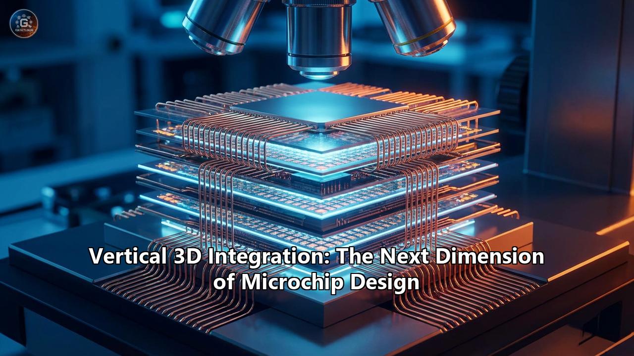
Vertical 3D integration is not merely a packaging technique; it is a fundamental architectural revolution. It represents the transition of the microchip from a flat city to a towering metropolis. By stacking active logic and memory layers directly on top of one another, engineers are unlocking bandwidths, efficiencies, and form factors that were physically impossible in the 2D era. This article explores the depths of this Z-axis revolution, detailing the technologies, the challenges, and the future of the chips that will power the next decade of human innovation.
Part 1: The End of Flat Earth—Why 3D?
To understand the necessity of 3D integration, one must first appreciate the "Interconnect Bottleneck." In modern high-performance computing (HPC) and AI processors, the transistor is no longer the primary limitation. The limitation is the wire.
As transistors shrank, they became faster. But the copper wires connecting them became thinner, more resistive, and more crowded. Moving data from one side of a large 2D chip to another takes time and energy—so much so that in some large AI clusters, moving data consumes more energy than processing it.
Vertical integration solves this by folding the 2D plane. Instead of sending a signal across a 20mm die, you send it up a few microns to the layer above. This reduces the interconnect length by orders of magnitude, slashing latency and power consumption (pJ/bit) simultaneously.
The Three Pillars of 3D Value:- Bandwidth: Vertical connections allow for thousands of wires to connect memory and logic, far exceeding the limits of the chip's edge.
- Heterogeneity: You can stack a logic die built on a cutting-edge 2nm node on top of an I/O die built on a mature, cheap 12nm node. This "mix-and-match" approach optimizes cost and yield.
- Form Factor: For mobile and edge devices, footprint is everything. 3D stacking allows desktop-class performance in wearable dimensions.
Part 2: The Toolkit—TSVs, Hybrid Bonding, and Monolithic 3D
The term "3D Integration" is an umbrella covering several distinct technologies, each offering different densities of vertical connectivity.
1. Through-Silicon Vias (TSVs)
The workhorse of the 3D era. A TSV is literally a vertical electrical connection (via) that passes completely through a silicon wafer or die.
- How it works: Holes are etched deep into the silicon, insulated, and filled with copper or tungsten. The wafer is then thinned down until the metal is exposed on the back, allowing it to connect to another die.
- Current State: TSVs are the backbone of High Bandwidth Memory (HBM), where 8 or 12 layers of DRAM are stacked. They typically have a pitch (spacing) of 40–50 microns, though advanced processes are pushing this down to 10 microns.
2. Hybrid Bonding (The Game Changer)
If TSVs are the elevator shafts, Hybrid Bonding is the teleporter. Traditional stacking uses "micro-bumps"—tiny solder balls—to connect dies. But solder has a limit; get too small, and it bridges, causing shorts.
- The Innovation: Hybrid bonding eliminates the bumps entirely. It polishes the copper interconnects and the dielectric (insulator) surface to near-perfect flatness. The two dies are then pressed together. The dielectric bonds instantly at room temperature (Van der Waals forces), and upon annealing (heating), the copper expands and fuses together.
- The Impact: This allows for interconnect pitches of under 10 microns, and eventually sub-1 micron. This density is high enough that you can split a single functional block (like an L3 cache) onto a separate vertical layer without a performance penalty. This is the technology behind AMD’s V-Cache and TSMC’s SoIC.
3. Monolithic 3D (Sequential Integration)
The Holy Grail. In TSV and Hybrid Bonding, you manufacture two separate wafers and glue them together. In Monolithic 3D, you build the first layer of transistors, seal it, and then grow a second layer of silicon crystal right on top of it to build more transistors.
- The Challenge: Making high-quality transistors requires heat (over 1000°C). If you heat the top layer that much, you melt the copper wiring in the bottom layer.
- The Solution: "Cool" fabrication techniques (like Laser Annealing) are being developed to create top-tier transistors without frying the basement. As of 2025, this is still largely in the research and early pathfinding phase but promises vertical connection densities equal to horizontal ones.
Part 3: The Chiplet Economy and UCIe 3.0
3D integration has given rise to the "Chiplet" model. Instead of designing one massive "System on Chip" (SoC) that is impossible to manufacture without defects, companies are breaking the design into smaller, modular functional blocks called chiplets.
- Yield Economics: A defect on a massive monolithic die kills the whole chip. A defect on a small chiplet only kills that chiplet. This dramatically improves yield and lowers costs.
- The Lego Ecosystem: You can buy a CPU chiplet from Intel, a GPU chiplet from NVIDIA, and an I/O chiplet from a third party, and stitch them together in a single package.
For chiplets to work, they need a standard language to talk to each other. Enter UCIe.
- Status Update (2025): The UCIe 3.0 specification, released in August 2025, has been a watershed moment. It introduced support for 64 GT/s data rates, doubling the bandwidth of the previous version. Crucially, UCIe 3.0 standardized protocols for 3D packaging, defining exactly how chiplets should communicate vertically through hybrid bonds, not just horizontally across an interposer. This standardization is creating an open market where "3D-ready" IP blocks can be bought off the shelf.
Part 4: Materials of the Future—The Rise of Glass Substrates
For decades, chips have sat on "organic" substrates—basically, high-tech reinforced plastic. But as we stack more and more chips, these plastic substrates are warping and bending under the heat and mechanical stress.
Enter Glass.In 2025, the industry began its aggressive pivot toward Glass Substrates, led by Intel and followed closely by Samsung and SKC.
- Flatness: Glass is incredibly flat and rigid. This is critical for hybrid bonding, where even a microscopic warp prevents the dies from touching perfectly.
- Thermal Stability: Glass doesn’t expand and contract with heat as much as plastic. This prevents the "shearing" of delicate vertical connections during operation.
- Interconnect Density: You can drill much finer holes (Through-Glass Vias or TGVs) in glass than in plastic, allowing for 10x denser connections between the chip and the motherboard.
By late 2025, pilot lines for glass substrates are active, with mass adoption expected to define the high-performance AI chips of 2026–2027.
Part 5: The Heat Wall—Cooling the Vertical City
The biggest enemy of 3D integration is heat. When you stack two high-power logic chips, the bottom chip is trapped. It has a ceiling (the top chip) that generates its own heat. How do you cool the bottom floor of a burning skyscraper?
Traditional air cooling and even standard liquid cold plates are no longer sufficient for these "thermal sandwiches."
Microfluidic Cooling (The 2025 Breakthrough):In late 2025, Microsoft and researchers unveiled a breakthrough in intrachip microfluidic cooling. Instead of putting a cold plate on the chip, they etched microscopic channels inside the silicon substrate itself.
- The Mechanism: Coolant flows directly through the chip, microns away from the hot transistors.
- The Result: This method demonstrated heat removal efficiencies 3x greater than traditional methods. It reduced peak temperatures by up to 65% in lab tests. This technology is the key enabler for stacking high-power logic on logic, which was previously considered thermally suicidal.
Part 6: The Titans of the Third Dimension
The battle for 3D supremacy is being fought by three main foundries, each with a distinct philosophy.
1. TSMC (Taiwan Semiconductor Manufacturing Company)- CoWoS (Chip-on-Wafer-on-Substrate): The current king of AI. It’s a 2.5D technology used by NVIDIA’s H100 and Blackwell GPUs. It sits chips side-by-side on a silicon interposer.
- SoIC (System on Integrated Chips): TSMC’s true 3D technology using hybrid bonding. It allows for "bumpless" stacking of logic and cache (used by AMD).
- Foveros: Intel’s 3D stacking technology. Foveros allows active logic dies to sit on top of a base die that acts as both an interposer and a functional chip (handling power delivery and I/O).
- PowerVia: While not strictly packaging, this "backside power delivery" technology cleans up the wiring mess, freeing up the front of the wafer for denser signal connections, making 3D stacking easier.
- X-Cube: Samsung’s 3D integration brand. They are leveraging their dominance in memory (DRAM/HBM) to create tightly coupled logic-memory stacks. They are aggressive on "Turnkey" solutions, offering to manufacture the memory, the logic, and do the 3D packaging all under one roof.
Part 7: The Future Horizon (2030 and Beyond)
As we look toward 2030, Vertical 3D Integration will evolve from a high-end luxury to a ubiquitous standard.
- Optical Interconnects (Silicon Photonics): Eventually, even copper vertical wires will be too slow or heat-generative. The industry is moving toward Co-Packaged Optics (CPO), where data is converted to light inside the 3D stack and shot out via optical fibers. This will decouple bandwidth from distance entirely.
- Neuromorphic 3D: The ultimate goal is to mimic the human brain. The brain is the ultimate 3D integrated circuit—a dense, 3D mesh of neurons and synapses with liquid cooling (blood) and chemical power delivery. Future 3D chips will adopt "synaptic" architectures, where memory and compute are not just stacked, but interwoven at the transistor level.
Conclusion
Vertical 3D Integration is not just the next step; it is the only step left. The days of easy scaling are behind us. The future belongs to the architects who can think in cubic millimeters rather than square ones. From the microscopic precision of hybrid bonding to the macroscopic shift to glass substrates, the industry is rebuilding itself around the Z-axis. We are witnessing the birth of the "Hyper-Moore" era—where performance scales not by shrinking, but by stacking. The skyline of silicon is rising.
Reference:
- https://www.photonics.com/Articles/UCIe-Consortium-Releases-Updated-Specification/a70205
- https://en.wikipedia.org/wiki/UCIe
- https://www.3dincites.com/2025/01/iftle-618-ucie-standard-vs-ucie-advanced-vs-ucie-3/
- https://chiplet-marketplace.com/news/ucie-2-0-specification
- https://www.design-reuse.com/news/202529142-ucie-consortium-introduces-3-0-specification-with-64-gt-s-performance-and-enhanced-manageability/
- https://iconnect007.com/article/137826/intel-unveils-industryleading-glass-substrates-to-meet-demand-for-more-powerful-compute/137823/smtahref
- https://www.trendforce.com/news/2025/09/10/news-intel-reportedly-reaffirms-glass-substrate-roadmap-pilot-line-rumored-in-2025/
- https://markets.financialcontent.com/wral/article/marketminute-2025-12-24-intels-18a-gamble-the-silicon-giants-final-stand-for-the-2026-ai-era
- https://markets.financialcontent.com/stocks/article/marketminute-2025-10-1-microsoft-unveils-microfluidic-cooling-breakthrough-a-new-era-for-ai-infrastructure
- https://news.microsoft.com/source/features/innovation/microfluidics-liquid-cooling-ai-chips/
- https://insidehpc.com/2025/09/microsoft-in-chip-microfluidics-improves-silicon-cooling-3x/
- https://www.yolegroup.com/industry-news/microfluidics-could-be-the-answer-to-cooling-ai-chips/
- https://www.intelmarketresearch.com/glass-core-substrates-2025-2032-459-6095
- https://www.digitimes.com/news/a20250709PD208/intel-glass-substrate-packaging-technology.html