Part I: The Missing Link in Flatland
The 2D Revolution and the "Metal Gap"
The history of materials science changed forever in 2004 with the isolation of graphene. By peeling a single layer of carbon atoms from a block of graphite using simple adhesive tape, Andre Geim and Konstantin Novoselov proved that two-dimensional (2D) materials were not just theoretical abstractions but physical realities. This discovery, which earned them the Nobel Prize in Physics, sparked a "gold rush" into the world of 2D materials—often referred to as "Flatland."
Over the next two decades, the family of 2D materials expanded rapidly. We discovered Transition Metal Dichalcogenides (TMDs) like Molybdenum Disulfide ($MoS_2$), which act as semiconductors perfect for transistors. We found Hexagonal Boron Nitride (h-BN), a superb insulator known as "white graphene." We even found magnetic 2D materials. But one major category was conspicuously absent from the 2D periodic table: Pure Metals.
Why 2D Metals Are So Difficult
Metals are the backbone of modern civilization, yet they are notoriously difficult to tame at the nanoscale. The reason lies in their atomic bonding.
- Layered vs. Non-Layered: Materials like graphite or $MoS_2$ are naturally layered. They consist of strong sheets of atoms held together by weak "Van der Waals" (vdW) forces—like a stack of slippery playing cards. It is easy to slide one card (layer) off the deck.
- The Metallic Bond: Pure metals, however, are 3D crystals held together by a "sea of electrons." This bonding is non-directional and isotropic; atoms want to be surrounded by neighbors on all sides. When you try to thin a metal down to a single atomic layer, surface tension takes over. The atoms instinctively clump together to minimize their surface energy, forming isolated islands or nanoparticles rather than a continuous flat sheet.
For years, scientists tried to deposit metal atoms onto substrates to form thin films, but they inevitably faced the "clumping" problem. The films would be polycrystalline, full of defects, or chemically bonded to the substrate, destroying the intrinsic "free-floating" nature that makes 2D materials so special. A true, free-standing, atomically thin metal seemed thermodynamically impossible.
Part II: The Breakthrough: Van der Waals Squeezing
In early 2025, a research team led by Professor Zhang Guangyu at the Institute of Physics, Chinese Academy of Sciences (IOP-CAS), shattered this barrier. Publishing their work in the journal Nature, they unveiled a technique that forces metals into submission not by chemical growth, but by brute force and elegant confinement. They called it Van der Waals Squeezing.
The Concept: A Molecular Vise
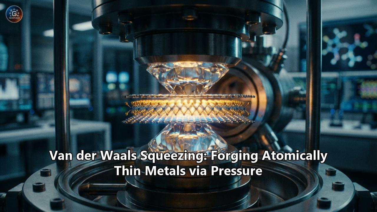
The genius of vdW squeezing lies in its simplicity. Instead of trying to grow a metal layer atom-by-atom (which allows time for clumping), the researchers take a bulk amount of metal, melt it, and then mechanically "squash" it into a 2D sheet before it has time to resist.
But you cannot just squeeze liquid metal between two glass slides; the surface roughness of glass is like a mountain range to an atom. You need surfaces that are atomically perfect.
- The Anvils: The team used "anvils" made of Molybdenum Disulfide ($MoS_2$) monolayers grown epitaxially on sapphire. $MoS_2$ is atomically flat—it has no dangling bonds, no surface roughness, and is chemically inert.
- The Process:
A small bead of low-melting-point metal (like Bismuth or Tin) is placed between two of these $MoS_2$ anvils.
The entire stack is heated until the metal melts.
Pressure is applied—specifically, around 200 MegaPascals (MPa). This is roughly the pressure found at the bottom of the deepest ocean trenches.
Under this immense pressure, the liquid metal is forced to spread out laterally. Because the $MoS_2$ walls are perfectly smooth and slippery (low friction), the metal glides effortlessly, thinning down until it reaches the ultimate limit: a single atomic layer.
The system is cooled while still under pressure, "freezing" the metal into this 2D state.
The Result: Angstrom-Scale Metals
The technique successfully produced continuous, single-crystal sheets of five different metals:
- Bismuth (Bi): ~6.3 Å thick
- Tin (Sn): ~5.8 Å thick
- Lead (Pb): ~7.5 Å thick
- Indium (In): ~8.4 Å thick
- Gallium (Ga): ~9.2 Å thick
To visualize this, if a standard sheet of paper were the $MoS_2$ anvil, the metal layer would be 100,000 times thinner than a coat of paint. These are not just thin films; they are quantum planes of metal atoms.
Part III: The Physics of Confinement
Why does this matter? When a material is squeezed from 3D to 2D, the laws of classical physics recede, and Quantum Mechanics takes the wheel. The electrons in these metals are no longer free to move in three dimensions; they are confined to a "quantum well" in the vertical direction.
1. Quantum Confinement and Band Structure
In a 3D metal, electron energy levels form continuous bands. In an atomically thin metal, confinement splits these bands into discrete sub-bands. This can fundamentally alter the material's identity.
- Semimetal to Semiconductor? Bulk Bismuth is a semimetal. In 2D form, gaps can open in its electronic structure, potentially turning it into a semiconductor or a topological insulator depending on the layer count.
- Enhanced Superconductivity: For superconductors like Tin, Indium, and Gallium, 2D confinement typically suppresses superconductivity due to thermal fluctuations. However, the $MoS_2$ encapsulation protects the Cooper pairs. In some cases, the reduced dimensionality can actually enhance the transition temperature ($T_c$) or create new pairing mechanisms driven by 2D phonon modes.
2. The "p-Type" Phenomenon
One of the most intriguing findings from the Zhang et al. study was that these encapsulated metals exhibit p-type behavior.
- Charge Transfer: The $MoS_2$ anvils are not just passive containers. $MoS_2$ is a semiconductor with a high electron affinity. When the metal layer (which has a high Fermi level) touches the $MoS_2$, electrons naturally flow from the metal into the $MoS_2$.
- Hole Doping: This loss of electrons leaves the metal layer with a surplus of "holes" (positive charge carriers).
- Significance: Creating p-type 2D metals is incredibly difficult. Most metal contacts to 2D semiconductors are n-type (electron donating), which creates high electrical resistance known as the "Schottky Barrier." The vdW squeezed metals, being intrinsically p-type due to this interface effect, could solve one of the biggest bottlenecks in 2D electronics: making efficient electrical contacts.
3. All-vdW Interfaces
The interface between the metal and the $MoS_2$ is "clean." In traditional metal deposition (evaporating hot gold onto silicon), the metal atoms crash into the surface, creating defects and chemical bonds. In vdW squeezing, the metal flows like a liquid over a slippery floor. There are no chemical bonds between the metal and the anvil—only weak van der Waals forces. This preserves the pristine crystalline quality of the metal, allowing electrons to travel long distances without scattering (high mobility).
Part IV: Material Spotlight
Let us look closer at the specific metals forged by this technique.
Bismuth (Bi): The Topological Star
Bismuth is the "heavyweight" of the group. Even in bulk, it is a weird metal—it is highly diamagnetic and has a low carrier density.
- In 2D: Monolayer Bismuth (often called Bismuthene) is predicted to be a 2D Topological Insulator. This means it conducts electricity perfectly along its edges (with zero resistance) while remaining insulating in its interior.
- Squeezing Victory: Previous attempts to grow Bismuthene required expensive molecular beam epitaxy (MBE) on specific substrates. The squeezing method produced Bismuth sheets over 100 micrometers wide—gigantic in the nano-world—making them usable for real device fabrication.
Gallium (Ga): The Shape-Shifter
Gallium is famous for melting in your hand (melting point ~29.7°C).
- Ga-liquid skin: The vdW squeezing technique exploits this low melting point perfectly.
- Superconductivity: 2D Gallium is a prime candidate for 2D Superconductivity. The confinement aligns the electron orbitals in a way that creates "flat bands"—energy states where electrons move slowly and interact strongly. Strong interaction is the recipe for high-temperature superconductivity.
Indium (In) and Tin (Sn)
Both are crucial for the electronics industry (Indium in touch screens, Tin in solder).
- Transparent Conductors: Indium Tin Oxide (ITO) is brittle. An atomically thin mesh of pure Indium or Tin could be flexible, transparent (because it's too thin to absorb light), and highly conductive. This is the "Holy Grail" for flexible smartphones and wearable screens.
Part V: Future Applications
The ability to mass-produce clean, atomically thin metals opens doors that were previously welded shut.
1. Quantum Computing (Josephson Junctions)
The heart of a superconducting quantum computer (like those built by Google or IBM) is the Josephson Junction—a sandwich of two superconductors separated by a thin insulator.
- The Problem: Current junctions rely on aluminum oxide barriers that are often "messy" and amorphous, introducing noise that kills the qubit's quantum state (decoherence).
- The Solution: A vdW squeezed metal could act as the superconductor, and a single layer of $MoS_2$ or h-BN could act as the barrier. Because the interfaces are atomically perfect, the resulting qubit could have significantly longer coherence times, accelerating the path to fault-tolerant quantum computing.
2. Post-Silicon Electronics
As silicon transistors reach their physical limits (Moore's Law is slowing down), the industry is looking at 2D semiconductors like $MoS_2$ and $WSe_2$.
- The Contact Resistance Problem: You can make a great 2D transistor, but if you can't get electricity in and out of it efficiently, it's useless. Standard 3D metal contacts don't touch 2D materials well.
- The vdW Contact: The squeezed metals are essentially "native" to the 2D world. Using a squeezed Bismuth layer to inject current into a $WSe_2$ transistor lowers the contact resistance by orders of magnitude. This could enable ultra-fast, low-power 2D chips.
3. Catalysis and Energy
In chemical reactions (like splitting water to make hydrogen fuel), surface area is everything.
- Maximum Surface: An atomically thin metal is all* surface. Every single atom is exposed to the environment.
- Activity: The unique electronic structure of these strained, confined metals can make them hyper-active catalysts. For example, 2D Indium might be far better at reducing $CO_2$ into useful fuels than bulk Indium.
Part VI: Challenges and Outlook
The Scalability Question
Currently, vdW squeezing is a lab-scale batch process. Squeezing one sample at 200 MPa takes time. For this to impact your iPhone, engineers need to develop a "roll-to-roll" version—perhaps passing metal and 2D films through high-pressure rollers like a pasta maker.
Alloys and Complexity
The initial study focused on pure elements. The next frontier is Alloys. Imagine squeezing a mix of Bismuth and Tellurium to create custom thermoelectric materials for energy harvesting. Or squeezing magnetic metals (like Iron or Cobalt) to create 2D magnets for spintronics. The researchers have already hinted that the technique works for alloys, opening a combinatorial playground of millions of new materials.
Conclusion: A New Tool for the Atomic Age
"Van der Waals Squeezing" is more than just a clever manufacturing trick; it is a conceptual leap. It teaches us that materials we thought we understood—simple metals like Lead or Tin—have secret lives that only emerge when they are pushed to the edge of existence. By applying pressure, we have not just flattened metals; we have expanded the horizon of physics.
As we move through 2025, we can expect to see these "Angstrom Metals" appearing in the first prototype devices, bridging the gap between the theoretical promise of the quantum world and the tangible reality of future technology.