The ability to detect and analyze light is the foundational pillar of modern technology, underpinning everything from the smartphone cameras in our pockets to the orbital telescopes peering into the cosmic dawn. Yet, for decades, the scientific community has been grappling with a fundamental physical compromise: we could either detect a very narrow slice of the electromagnetic spectrum at incredibly high speeds, or we could detect a broad range of frequencies at a painfully slow pace.
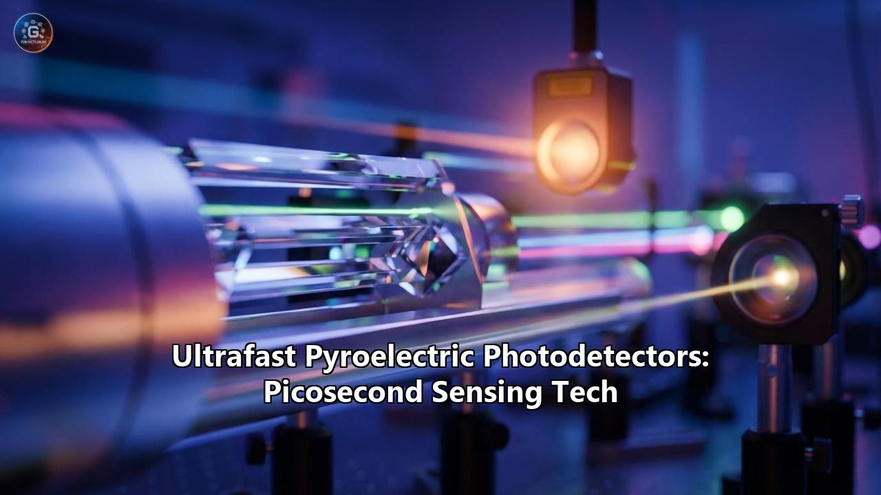
However, an epoch-defining leap in nanoscale engineering has recently shattered this longstanding barrier. In early 2026, researchers at Duke University unveiled an ultrafast pyroelectric photodetector capable of sensing light across the entire electromagnetic spectrum with a staggering response time of just 125 picoseconds. Operating at speeds up to 2.8 gigahertz, this device is hundreds to thousands of times faster than conventional thermal detectors, definitively rewriting the rules of optoelectronics.
To comprehend the sheer magnitude of this breakthrough—and its far-reaching implications for autonomous vehicles, medical diagnostics, space exploration, and quantum communication—we must embark on a deep dive into the physics of light detection, the intricacies of the pyroelectric effect, and the "plasmonic magic" of modern metasurfaces.
The Physics of Catching Light: Semiconductors vs. Thermal Detectors
To appreciate the revolution brought about by picosecond sensing technology, it is essential to understand the historical divide in photodetection mechanisms. Photodetectors broadly fall into two categories: photon-driven (semiconductor) detectors and thermally-driven detectors.
The Semiconductor Speed LimitMost modern imaging systems, such as the CMOS sensors in digital cameras, rely on the photoelectric effect within semiconductor materials. When an incoming photon strikes the semiconductor, it transfers its energy to an electron. If the photon possesses enough energy to overcome the material's "bandgap"—the energy difference between the valence band and the conduction band—the electron is knocked loose, creating a measurable electrical current.
Semiconductor detectors are exceptionally fast, easily achieving nanosecond to picosecond response times. However, they are inherently restricted by their bandgaps. A silicon sensor, for instance, is highly sensitive to visible light but becomes entirely blind to lower-energy infrared or terahertz waves, because those photons simply do not pack enough punch to vault electrons across the bandgap. To detect mid-infrared or long-wave infrared light using semiconductors, engineers must use exotic materials with very narrow bandgaps, such as Mercury Cadmium Telluride (HgCdTe). The fatal flaw of narrow-bandgap materials is that at room temperature, ambient thermal energy is enough to excite electrons, drowning the sensor in "dark current" noise. Consequently, these high-speed infrared sensors require bulky, expensive, and power-hungry cryogenic cooling systems.
The Thermal Alternative and Its Historic SluggishnessThermal photodetectors provide a radically different approach. Instead of relying on bandgap excitation, these devices absorb incoming radiation, convert it into heat, and then measure the resulting temperature change to generate an electrical signal. Because any electromagnetic wave—from high-energy gamma rays to low-energy radio waves—can be absorbed and converted into heat, thermal detectors are inherently "broadband." They can operate at room temperature without the need for cryogenic cooling.
There is, however, a massive catch: thermodynamics. Traditional thermal detectors (like bolometers and standard pyroelectric sensors) are agonizingly slow. Heating up a macroscopic piece of material, waiting for that heat to diffuse through the sensor, and then waiting for the material to cool down before it can detect the next pulse of light is a process that typically takes microseconds or even milliseconds. In the fast-paced world of optical communications and autonomous LiDAR (Light Detection and Ranging), a millisecond delay is an eternity.
Unpacking the Pyroelectric Phenomenon
To bridge the gap between broadband sensitivity and high-speed operation, researchers turned to a specific class of thermal sensing known as the pyroelectric effect.
Pyroelectricity is a property exhibited by certain non-centrosymmetric crystals, such as Aluminum Nitride (AlN), Lithium Tantalate (LiTaO₃), and various polymer films. These materials possess a natural, spontaneous internal electrical polarization; their positive and negative charge centers do not perfectly overlap, creating built-in electrical dipoles.
When a pyroelectric material is subjected to a change in temperature, its crystal lattice expands or contracts. This subtle structural deformation shifts the positions of the atoms, momentarily altering the material's internal polarization. The sudden shift in polarization drives a rapid displacement current to the surface electrodes, resulting in a measurable voltage spike.
Crucially, pyroelectric detectors do not measure absolute temperature—they measure the rate of change in temperature. If you shine a steady, continuous beam of light onto a pyroelectric sensor, it will generate a brief signal when the light turns on, and then the signal will fade to zero as the temperature stabilizes. This makes them exceptionally adept at detecting rapid pulses, varying signals, and chopped light, which are the exact requirements for high-speed optical data transmission and time-of-flight LiDAR systems.
Yet, despite this advantageous characteristic, conventional pyroelectric detectors still relied on thick, bulky light-absorbing layers. The heat had to physically travel through these thick layers before reaching the pyroelectric crystal, imposing a strict limit on how fast the device could respond.
The Metasurface Miracle: Trapping Light at the Nanoscale
The turning point in thermal detection arrived when researchers stopped trying to optimize the bulk materials and instead manipulated light at the molecular scale. The 2026 Duke University breakthrough, spearheaded by Professor Maiken H. Mikkelsen and her team, achieved its unprecedented 125-picosecond speed by integrating an ultrathin pyroelectric layer with a meticulously engineered "metasurface".
The Architecture of a Light TrapA metasurface is an artificial material engineered to possess properties not found in nature, utilizing structures that are smaller than the wavelength of the light they are designed to manipulate. The Duke team's metasurface acts as a "perfect absorber," trapping nearly 100% of incoming light and instantly converting it into localized heat.
The anatomy of this record-breaking device is a marvel of nanofabrication:
- The Base Reflector: A thin sheet of gold sits at the bottom, acting as a mirror.
- The Dielectric Gap: Above the gold is an incredibly thin, 10-nanometer transparent layer.
- The Plasmonic Resonators: Precisely arranged silver nanocubes are positioned on top of the transparent layer.
- The Pyroelectric Transducer: Beneath the metasurface lies an ultrathin film of pyroelectric material, such as Aluminum Nitride.
When incident light strikes the silver nanocubes, it interacts with the free electrons on the surface of the metal. If the frequency of the light matches the resonant frequency of the nanocubes (which can be tuned by altering the size and spacing of the cubes), it triggers a phenomenon known as Localized Surface Plasmon Resonance (LSPR).
The light's electromagnetic field forces the electrons in the silver to oscillate violently. This interaction essentially "traps" the photon's energy in the microscopic 10-nanometer gap between the nanocube and the gold film. Because the energy is squeezed into such an impossibly tiny volume, the localized surface plasmons decay at femtosecond (quadrillionths of a second) time scales. As they decay, the kinetic energy of the electrons is converted into intense, highly localized heat through a process called electron-phonon scattering.
Because the entire light-trapping and heating process occurs on a scale of just tens of nanometers, the heat does not need to slowly diffuse through a thick bulk material. It is instantly transferred to the adjacent ultrathin pyroelectric layer.
Circumventing the RC DelayGenerating the heat quickly was only half the battle; the team also had to extract the electrical signal before it degraded. In electronics, the speed of a device is often constrained by its RC (Resistor-Capacitor) time constant. To minimize this electrical bottleneck, the researchers redesigned the metasurface into a circular configuration. This geometry maximized the area exposed to light while drastically minimizing the physical distance the electrical signal had to travel to reach the readout circuitry.
To definitively prove the speed of their invention, doctoral candidate Eunso Shin employed a rigorous experimental setup utilizing dual distributed feedback lasers. By modulating the lasers at incredibly high frequencies and measuring the beat signals, they verified that the device possessed a 3 decibel (dB) bandwidth of 2.8 gigahertz.
At that frequency, the detector was successfully translating incoming light into an electrical spike in exactly 125 picoseconds. To put this in perspective, 125 picoseconds is one-eighth of a billionth of a second—faster than many fundamental chemical reactions, and a speed previously thought to be the exclusive domain of narrow-bandgap semiconductors. Finite-element thermodynamic simulations conducted by the team suggest that with further optimization of the active area, the fundamental thermal limits of this architecture could reach an astonishing 25 to 30 picoseconds.
Pyroelectric-Accelerated Perovskites: A Parallel Revolution
While the metasurface approach has redefined pure thermal detectors, another groundbreaking strategy emerged concurrently in the realm of hybrid optoelectronics. Researchers recognized that the rapid polarization shift inherent to the pyroelectric effect could be weaponized to accelerate other, sluggish materials.
A prime example is the integration of pyroelectricity with halide perovskites. Perovskites are a class of materials with a specific crystal structure that have recently taken the solar cell and LED industries by storm due to their exceptional light-absorbing capabilities, adjustable direct bandgaps, and low-cost fabrication. However, when used in photodetectors, bulky perovskite devices often suffer from charge recombination—electrons and holes generated by the light recombine before they can be collected as a current, severely limiting response times and sensitivity.
In a landmark study published in Advanced Materials, researchers including Liangliang Min and Liang Li demonstrated a "Pyroelectric-Accelerated Perovskite Photodetector". By interfacing a perovskite light-absorbing layer with a pyroelectric material, they created a synergistic device.
When a laser pulse hits the perovskite, it simultaneously generates electron-hole pairs (the photoelectric effect) and slightly heats the device. The transient heat triggers the pyroelectric layer, which instantly generates a massive, temporary internal electric field via spontaneous polarization. This sudden burst of internal voltage acts like an electrical vacuum cleaner, violently sweeping the photo-generated electrons and holes apart before they have a chance to recombine.
This pyroelectric acceleration drastically boosts the extraction efficiency of the charge carriers. The result is a self-powered device exhibiting an external quantum efficiency exceeding 100% and a response speed measured in nanoseconds to picoseconds, all without the need for the high, energy-consuming external bias voltages required by traditional avalanche photodiodes.
Bridging the Terahertz Gap
The true value of ultrafast broadband photodetection becomes apparent when we look at the "Terahertz Gap". The terahertz (THz) band of the electromagnetic spectrum sits snugly between microwave and infrared frequencies (roughly 0.1 to 10 THz).
For decades, the terahertz band was practically inaccessible. Electronic components (like those used in radar and Wi-Fi) were too slow to generate or detect THz frequencies, while optical devices (like lasers and semiconductor sensors) lacked the narrow-bandgap materials required to operate at such low photon energies without extreme cryogenic cooling.
Yet, THz radiation holds almost mythical properties for industrial and scientific applications:
- Non-Ionizing: Unlike X-rays, THz radiation does not possess enough energy to strip electrons from atoms, making it completely safe for human tissue scanning.
- Deep Penetration: THz waves pass easily through plastics, clothing, paper, and ceramics, but are strongly absorbed by water and metals.
- Chemical Fingerprinting: Many complex molecules, including explosives, narcotics, and pharmaceutical compounds, have unique rotational and vibrational resonances in the THz band, allowing for distinct spectral signatures.
Because the picosecond pyroelectric detectors operate on heat rather than bandgaps, they are completely agnostic to the photon energy. They can detect THz radiation just as easily as they detect visible light, operating at room temperature with zero external power.
This capability is poised to ignite the global terahertz technology market, which industry analysts project will surpass $1.48 billion by 2026, driven by an impressive compound annual growth rate (CAGR) of over 25%. From airport security scanners that can identify the exact chemical composition of concealed powders, to pharmaceutical quality control lines that use THz pulses to verify the crystalline structure and coating thickness of pills in real-time, the commercial applications are immense.
Transformative Applications of Picosecond Thermal Sensing
The transition from microsecond to picosecond thermal sensing is not merely an academic milestone; it is an enabling technology that will cascade across multiple industries, unlocking capabilities that were previously confined to the realm of science fiction.
1. Next-Generation LiDAR and Autonomous Vehicles
Light Detection and Ranging (LiDAR) is the "vision" system for autonomous vehicles, drones, and advanced robotics. LiDAR systems work by firing a laser pulse at a target and measuring the exact time it takes for the light to bounce back. Because light travels at roughly 300,000 kilometers per second, precise distance measurement requires photodetectors with extreme temporal resolution.
Currently, autonomous vehicles rely on silicon or indium gallium arsenide (InGaAs) avalanche photodiodes. These are expensive, fragile, require high operating voltages, and often struggle in adverse weather conditions like dense fog or dust, which scatter standard near-infrared lasers.
Ultrafast pyroelectric and pyroelectric-accelerated perovskite photodetectors offer a disruptive alternative. Because they can operate at 125-picosecond speeds, they provide time-of-flight resolution capable of millimeter-to-centimeter level accuracy. More importantly, their broadband nature allows LiDAR systems to easily shift to longer mid-infrared or THz wavelengths, which suffer from significantly less Rayleigh scattering and can effortlessly pierce right through fog, smoke, and atmospheric dust.
2. Multispectral Medical Diagnostics and Imaging
The human body is highly transparent to certain bands of infrared and terahertz light, making broadband sensing a holy grail for non-invasive medical diagnostics.
Currently, detecting skin anomalies or subcutaneous tumors requires physical biopsies or ionizing radiation. With ultrafast room-temperature pyroelectric detectors, doctors can utilize compact multispectral cameras. By pulsing various wavelengths of harmless infrared and THz light onto a patient's skin and capturing the high-speed thermal/optical reflections, these cameras can map blood flow, monitor tissue oxygenation, and identify the chemical signatures of malignant melanoma cells in real time. Furthermore, because the sensors require no cryogenic cooling, they can be miniaturized into handheld diagnostic wands for point-of-care environments.
3. Space Exploration and Astronomy
Astrophysics relies heavily on observing the universe across the entire electromagnetic spectrum. The cosmic microwave background, cold interstellar dust clouds, and distant redshifted galaxies emit most of their energy in the far-infrared and terahertz bands.
Historically, deploying infrared telescopes into space (such as the Herschel Space Observatory or the James Webb Space Telescope) required massive, complex, and highly restrictive liquid helium or mechanical cryocooling systems to keep the sensors close to absolute zero. If the coolant runs out, the multi-billion-dollar telescope effectively goes blind.
The advent of highly sensitive, picosecond-speed thermal photodetectors that operate at room temperature radically alters the economics and lifespan of space-based sensing. Future orbital observatories and planetary probes could be equipped with lightweight, uncooled multispectral arrays, dramatically reducing payload weight and extending mission durations indefinitely.
4. Hyperspectral Agriculture and Food Safety
Modern agriculture is increasingly reliant on data to optimize yields and minimize resource waste. Hyperspectral imaging—capturing imagery across dozens or hundreds of specific electromagnetic bands simultaneously—allows farmers to assess the exact chemical composition of their crops.
Traditional hyperspectral cameras are bulky, combining multiple different sensor types (silicon for visible, InGaAs for short-wave infrared) to cover a wide spectrum. A single array of metasurface-enhanced pyroelectric pixels, however, can act as an on-chip spectral filter. By varying the size and spacing of the silver nanocubes across different pixels on a single chip, engineers can create a monolithic sensor where every pixel is tuned to absorb a different, highly specific frequency of light—from ultraviolet to mid-infrared. Mounted on agricultural drones, these ultrafast sensors could scan thousands of acres per hour, instantly detecting early signs of crop stress, pinpointing exact hydration levels, and identifying chemical markers of fungal infections before they become visible to the naked eye.
5. Ultrafast Optical Communications and Quantum Tech
The insatiable global demand for data bandwidth is pushing optical communications into new frontiers. While fiber optics handle long-distance data well, free-space optical communication (transmitting data via lasers through the air or space) requires receivers capable of operating at gigahertz modulation speeds while simultaneously rejecting ambient light noise.
The 2.8 gigahertz bandwidth of the Duke University photodetector is a milestone for optical data transmission. Because the metasurface inherently acts as a perfect, narrow-band spectral filter, it only absorbs the exact frequency it is engineered to target, effectively ignoring background solar radiation. This makes it an ideal candidate for high-speed, secure free-space optical communication links between satellites, or between buildings in dense urban environments.
Additionally, Professor Mikkelsen's work with plasmonic nanogap cavities extends deeply into quantum technologies, including the creation of ultrabright single-photon sources. The ability to manipulate light-matter interactions at the picosecond scale is fundamental to the development of quantum communication networks and photonic quantum computers, which require the high-speed emission and detection of individual photons without thermal decoherence.
Engineering the Future: Challenges and On-Chip Integration
While the demonstration of a 125-picosecond pyroelectric photodetector is a monumental scientific triumph, transitioning this technology from the laboratory to mass-market commercialization presents its own set of engineering challenges.
The Responsivity vs. Speed TradeoffIn detector design, there is always a tug-of-war between speed and responsivity (the electrical output per unit of optical input power). Smaller active areas dramatically boost speed by reducing the electrical capacitance (the RC time constant). The Duke prototype utilized tiny active areas—between 20 and 60 micrometers in diameter—to achieve its 2.8 GHz speeds. However, a smaller active area captures less overall light, which trims the responsivity.
To counteract this, noise equivalent power (NEP) must be minimized. The advanced circuitry and highly crystalline pyroelectric thin films used in recent prototypes have pushed the NEP down to 96 picowatts per square root hertz. This makes the device highly competitive with pricier, cooled alternatives, but scaling up to larger sensor arrays while maintaining gigahertz speeds will require innovative read-out integrated circuit (ROIC) designs to manage localized capacitance.
CMOS Compatibility and FabricationFor a new sensing technology to truly change the world, it must be compatible with existing semiconductor manufacturing infrastructure. The beauty of the metasurface-pyroelectric design lies in its materials: silver, gold, and aluminum nitride are all standard materials within the global CMOS (Complementary Metal-Oxide-Semiconductor) fabrication ecosystem.
Unlike growing exotic crystalline structures like HgCdTe, which requires highly specialized foundries, depositing 10-nanometer dielectric layers and patterning silver nanocubes can be achieved using scalable techniques like nanoimprint lithography and atomic layer deposition (ALD). This opens a clear pathway to mass-producing megapixel, high-speed thermal imaging arrays at a fraction of the cost of current infrared technologies.
A New Era of Sensing
For over a century, the scientific community accepted the sluggishness of thermal detection as an immutable law of nature—an inescapable penalty for the luxury of broad-spectrum sensitivity. The arrival of picosecond pyroelectric photodetectors decisively shatters this paradigm.
By seamlessly weaving together the quantum mechanical marvels of plasmonics, the thermodynamic properties of nanoscale gaps, and the spontaneous polarization of pyroelectric crystals, researchers have forged a technology that bridges the deepest divides in optoelectronics. At 125 picoseconds, we are no longer merely measuring the slow accumulation of heat; we are listening to the instantaneous, femtosecond whispers of electron-phonon scattering and capturing the exact moment light yields its energy to matter.
As this technology matures, moving from isolated laboratory proofs-of-concept to highly integrated, CMOS-compatible arrays, the ripple effects will be felt across every discipline of modern science and engineering. We are standing on the precipice of a new era of sensing, an era where the invisible universe—from the chemical signatures of living tissue to the terahertz echoes of deep space—will finally be revealed to us in real-time, high-definition clarity.
Reference:
- https://ouci.dntb.gov.ua/en/works/400BO2YP/
- https://teacher.yzu.edu.cn/MLL/zh_CN/zhym/527229/list/index.htm
- https://www.sciencedaily.com/releases/2026/03/260304184218.htm
- https://pub.confit.atlas.jp/en/event/opic2026/session/2ALPS-304-07
- https://orcid.org/0000-0003-0708-7762
- https://www.prnewswire.com/news-releases/the-worldwide-terahertz-technology-industry-is-expected-to-reach-1-4-billion-by-2026--301408657.html
- https://www.mdpi.com/2079-4991/15/11/816
- https://www.optica.org/events/topical_meetings/ultrafast_phenomena/about/