Extreme Ultraviolet (EUV) lithography represents a pivotal technology in modern semiconductor manufacturing, driving the industry's ability to produce increasingly smaller, faster, and more power-efficient chips. This advanced technique uses light with an extremely short wavelength of 13.5 nanometers (nm), significantly smaller than the 193 nm light used in traditional Deep Ultraviolet (DUV) lithography. This shorter wavelength allows manufacturers to etch much finer patterns onto silicon wafers, a necessity for creating transistors at the 7nm node and beyond, including current 5nm and 3nm processes.
The Role of EUV in Advancing Moore's LawEUV technology is fundamental to continuing the trend described by Moore's Law, which observes the doubling of transistor density on integrated circuits roughly every two years. By enabling the printing of smaller features, EUV directly supports this miniaturization trend. This increased transistor density leads to chips with enhanced performance and reduced power consumption, vital for applications ranging from smartphones and AI processors to autonomous vehicles and advanced memory technologies. Leading chipmakers like TSMC, Samsung, Intel, SK hynix, and Micron are already utilizing EUV in high-volume production for critical layers of their most advanced logic and memory chips. EUV simplifies manufacturing compared to multi-patterning DUV techniques, reducing the number of masking layers required, which can improve production efficiency and yield.
Challenges and Ongoing DevelopmentsDespite its advantages, EUV lithography faces significant challenges:
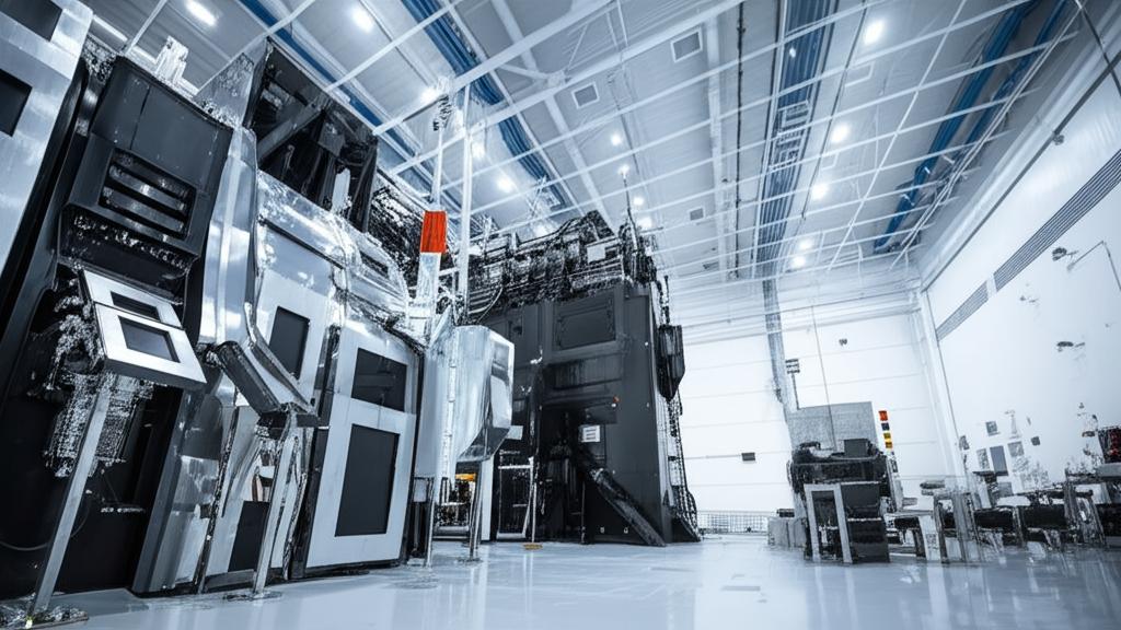
- Cost: EUV machines, solely supplied by ASML, are extremely expensive, with each unit costing upwards of $150 million. Their high power consumption also translates to significant operational costs.
- Complexity: EUV systems require a complex infrastructure, including high-power laser-produced plasma (LPP) sources to generate the 13.5 nm light and reflective optics (multilayer mirrors) operating in a vacuum, as EUV light is absorbed by almost all materials, including air.
- Source Power and Throughput: Generating sufficient EUV light efficiently remains a challenge. While source power has improved, continuous efforts are needed to boost power further (targeting beyond 250W) to increase wafer throughput (wafers per hour) and make the technology more cost-effective. Researchers are exploring alternative laser sources, like diode-pumped solid-state lasers (DPSSLs), which could be 5-10 times more efficient than current CO2 laser systems.
- Mask Infrastructure: EUV uses reflective masks, which are susceptible to defects. Even microscopic flaws can distort the reflected light, impacting yield. Innovations in mask inspection, defect-free mask blanks, and multi-beam mask writers are crucial.
- Photoresists: Developing photoresist materials that offer high resolution, sensitivity (requiring lower exposure dose), and low line-edge roughness (LER) is an ongoing area of intense research.
To push miniaturization even further, the industry is moving towards High-Numerical Aperture (High-NA) EUV lithography. By increasing the numerical aperture (NA) of the projection optics from 0.33 (standard EUV) to 0.55, High-NA EUV systems enable even higher resolution, targeting feature sizes down to 8 nm. This is critical for manufacturing nodes below 2nm, such as the 1.4nm (A14) and potentially 1nm (A10) nodes.
ASML delivered the first High-NA EUV system (EXE:5000) in late 2023, with high-volume manufacturing using these tools expected to start around 2025-2026. Intel is an early adopter, planning to use High-NA EUV for its 14A node. TSMC also received its first High-NA machine in late 2024 and plans to integrate it into its A14 node, expected around 2027. While significantly more expensive (estimated around $384 million per machine), High-NA EUV offers the potential to reduce process steps compared to multi-patterning techniques with standard EUV, potentially improving cost, yield, and cycle time for future nodes.
Looking further ahead, ASML has even revealed roadmaps for "Hyper-NA" EUV systems with a 0.75 NA, potentially enabling process nodes below 0.2nm (2 angstroms) sometime after 2030.
The Future LandscapeEUV and its successor, High-NA EUV, are set to remain the cornerstones of leading-edge semiconductor manufacturing for the foreseeable future, enabling continued scaling for demanding applications like AI, high-performance computing, and advanced mobile devices. While DUV lithography will continue to be used for less critical layers due to cost-effectiveness, EUV is indispensable for the most intricate patterns. The successful deployment and maturation of High-NA EUV, along with ongoing efforts to improve the efficiency, cost, and supporting ecosystem (masks, resists) of EUV technology, will dictate the pace of innovation in the semiconductor industry for the next decade and beyond. Other technologies like directed self-assembly (DSA) and potentially multi-beam electron lithography may also play complementary roles alongside EUV. The journey requires continuous breakthroughs and significant investment but is essential for powering our increasingly digital world.