If you were to shrink yourself down to the size of a bacterium, the world would become a strange and hostile place. The rules of gravity would fade, replaced by the sticky, overwhelming forces of surface tension and van der Waals interactions. In this alien landscape, traditional manufacturing tools—drills, lathes, molds—are useless. They are simply too clumsy, too brutal, and too large. Yet, it is precisely here, in this sub-micron realm, that the future of medicine, computing, and materials science is being forged.
For decades, the ability to build complex, three-dimensional structures at this scale was a dream. We could etch flat patterns onto silicon chips, but true 3D manufacturing—the ability to build intricate lattice towers, functional micro-turbines, or scaffolds for living cells—remained out of reach. That is, until the mastery of a phenomenon known as Two-Photon Polymerization (2PP).
2PP is not merely "3D printing for small things." It is a fundamental rethinking of how we manipulate matter with light. By harnessing the nonlinear quantum optics of femtosecond lasers, engineers can now solidify liquid resin at a resolution that defies the traditional diffraction limits of light itself. We are no longer just printing; we are sculpting with photons, creating architectures so fine that they are invisible to the naked eye but strong enough to change the world.
Part I: The Physics of the Impossible
To understand why 2PP is revolutionary, one must first appreciate the limitations of the tools that came before it. Traditional stereolithography (SLA), the grandfather of light-based 3D printing, works on a principle of "one-photon absorption." A laser beam of ultraviolet (UV) light traces a shape on the surface of a vat of liquid resin. Wherever the beam hits, the resin absorbs a photon, a chemical bond breaks, and the liquid turns into a solid polymer.
The problem with this method is that the absorption happens everywhere the light touches. As the laser beam travels through the resin, it cures the material all along its path, like a flashlight beam freezing water into ice. This limits you to building layer by layer, from the bottom up, with significant constraints on geometry and resolution.
Two-Photon Polymerization changes the game by exploiting a loophole in quantum mechanics.
The Quantum Loophole: Two-Photon Absorption
In 1931, Nobel laureate Maria Goeppert-Mayer predicted a phenomenon that seemed purely theoretical at the time. She theorized that an atom or molecule could absorb two photons simultaneously in a single quantum event, provided they arrived within a fraction of a femtosecond (one quadrillionth of a second) of each other. The combined energy of these two less energetic photons (usually in the near-infrared spectrum) would equal the energy of one high-energy photon (in the UV spectrum) needed to trigger a chemical reaction.
This "simultaneity" is the key. In a 2PP system, the laser used is typically a near-infrared femtosecond laser. The resin used is transparent to this infrared light. When the laser beam passes through the resin, nothing happens—the photons are too weak individually to trigger polymerization. The light simply passes through the liquid like sunlight through a window.
However, researchers use a high-numerical-aperture lens to focus this laser beam into a vanishingly small point. At this focal point—and only at this focal point—the density of photons becomes astronomically high. For a fleeting instant, the probability of a molecule getting hit by two photons at the exact same time skyrockets. The resin molecule absorbs the combined energy, becomes excited, and initiates the polymerization reaction.
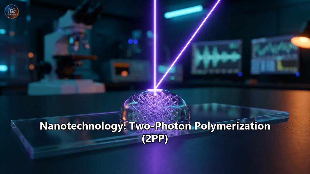
The Voxel: A Solid Point of Light
The result is magical. Instead of a beam that hardens everything in its path, you have a "voxel" (volumetric pixel) of solid plastic that forms floating deep inside the liquid resin. The material above and below the focal point remains liquid.
This "spatial confinement" allows for true 3D writing. You are not bound to layers. You can move the laser focus in any direction—up, down, left, right, diagonal—drawing free-form structures inside the volume of the material. It is akin to moving a pen through the air and having the ink solidify instantly in 3D space.
Furthermore, because the two-photon absorption effect depends on the square of the light intensity, the reaction volume is even smaller than the focused spot of the laser itself. By carefully controlling the laser power near the threshold of polymerization, engineers can create features as small as 100 nanometers—hundreds of times thinner than a human hair.
Part II: The Machinery of Creation
The hardware required to orchestrate this quantum dance is a marvel of modern engineering, evolving rapidly from optical tables in university basements to sleek, industrial-grade desktop machines in 2024 and 2025.
The Heartbeat: Femtosecond Lasers
The engine of a 2PP system is the femtosecond laser. These devices emit pulses of light that last only 100 to 200 femtoseconds. To visualize this timescale: a femtosecond is to a second what a second is to about 31.7 million years.
These ultra-short pulses are necessary to pack enough photons into a brief moment to trigger the two-photon effect without boiling the resin. If you used a continuous wave laser with the same average power, you would simply heat up the liquid. The "pulsed" nature allows for peak intensities of terawatts per square centimeter—intensities usually found in nuclear explosions—but only for such a short time that the material doesn't burn; it just chemically reacts.
The Hands: Galvo Mirrors and Piezo Stages
Directing this laser focus requires extreme precision. Early systems moved the sample stage using piezoelectric motors, which are incredibly precise but slow. Modern systems, such as those developed by leaders like Nanoscribe (now part of BICO) and UpNano, utilize a hybrid approach.
High-speed galvanometer mirrors (galvos) deflect the laser beam to scan the "fast" axes (X and Y), writing a slice of the structure at lightning speeds. Meanwhile, a piezo stage moves the sample in the Z-axis (and sometimes X and Y for larger stitching) to position the writing volume.
In 2024 and 2025, a major leap occurred in writing speeds. While early systems wrote at millimeters per second, new "holographic multi-foci" techniques have shattered these limits. By passing the laser beam through a Spatial Light Modulator (SLM), the single beam is split into a hologram of dozens, or even hundreds, of focal points. These "ghost pens" write simultaneously, increasing throughput by orders of magnitude. A recent breakthrough reported in Nano Letters in 2024 demonstrated a system writing at over 149 million voxels per second, creating complex millimeter-scale structures in seconds rather than hours.
The Brain: AI and Slicing Algorithms
Software has become just as critical as hardware. Writing at the nanoscale introduces challenges that don't exist in macro 3D printing. As the resin polymerizes, it shrinks slightly, which can cause delicate nanostructures to warp or collapse.
By 2026, "smart slicing" software has become the standard. These programs use Deep Reinforcement Learning (DRL) to predict how the material will behave during the print. They automatically adjust the laser power, writing speed, and pathing to compensate for shrinkage and optical aberrations.
For instance, when writing deep inside a thick layer of resin, the refractive index mismatch can distort the laser focus, making it look like a comet rather than a sphere. New AI-driven "aberration correction" modules dynamically alter the wavefront of the laser to keep the focus sharp, regardless of how deep into the material the printer is working. This has effectively doubled the printable height of many microstructures.
Part III: The Materials Revolution
The "ink" used in 2PP is just as sophisticated as the printer. Initially, researchers used standard photoresists from the semiconductor industry (like SU-8), which were rigid and brittle. Today, the palette of materials is vast and functional.
The Rise of Bio-Resins
One of the most significant trends of the 2024-2026 period has been the explosion of biocompatible resins. Standard industrial resins are often cytotoxic—they kill cells. For biomedical applications, the material must be friendly to life.
New hydrogel-based resins, such as modified Gelatin Methacryloyl (GelMA) and Hyaluronic Acid derivatives, allow for the printing of scaffolds that mimic the softness and water content of natural tissue. These materials are "tunable," meaning their stiffness can be adjusted to match bone, cartilage, or brain tissue.
A breakthrough in late 2024 saw the introduction of "UpNano Green," a system utilizing a 515 nm green laser instead of the traditional 780 nm infrared. This wavelength shift was crucial because it allowed the polymerization of new classes of bio-materials that were previously transparent or unresponsive to infrared light. This opened the door to printing with proteins and enzymes directly, without denaturing them.
Hybrid and Functional Materials
It's not just about structure; it's about function.
- Piezoelectric Resins: We can now print materials that generate electricity when squeezed. This allows for the creation of microscopic sensors and energy harvesters that power themselves from the vibrations of blood flow or sound waves.
- Conductive Polymers: While printing pure metal via 2PP is difficult (though possible via photoreduction), conductive polymers allow for the direct writing of electrical circuits at the microscale.
- Shape-Memory Polymers (4D Printing): These materials change shape when exposed to heat, pH changes, or light. A 2025 study demonstrated "4D printed" micro-grippers that are printed in an "open" state but snap shut when introduced to a specific acidic environment—like a tumor microenvironment—to release a drug payload.
Part IV: Biomedical Frontiers
The killer application for 2PP has undoubtedly been in medicine. The ability to structure matter at the same scale as cells (10-100 microns) and sub-cellular components (1-10 microns) has bridged the gap between biology and engineering.
Organ-on-a-Chip: The End of Animal Testing?
"Organ-on-a-chip" devices are microfluidic chips that simulate the activities of human organs. They contain tiny channels lined with living human cells. The challenge has always been recreating the complex, fractal-like network of blood vessels (vasculature) that keeps real organs alive.
Traditional manufacturing cannot make 3D micro-capillaries. 2PP can. In 2025, researchers at Missouri S&T unveiled a "one-pot" resin method that allows for the rapid printing of highly branched, porous blood vessel networks inside a chip. By flowing nutrients through these 2PP-printed capillaries, they kept thick liver tissue constructs alive for weeks, allowing for drug toxicity testing that is far more accurate than animal models.
The Fantastic Voyage: Micro-Robotics
Perhaps the most sci-fi application is the "micro-robot." These are not mechanical droids with gears and batteries, but chemically or magnetically driven architectures.
In 2025, a team created "light-driven" microrobots using 2PP. These helical swimmers, coated with a thin layer of metal, can be steered through fluids using external magnetic fields. But the breakthrough was the cargo handling. Using laser-induced convection currents (controlled heating of the water around the bot), these robots could "trap" a single drug molecule or cell, transport it to a specific location in a petri dish, and release it.
Imagine a swarm of thousands of these 2PP-printed bots injected into the bloodstream, guided magnetically to a blood clot, and mechanically drilling through it to restore flow. This is no longer pure fantasy; the prototypes are swimming in labs today.
Neural Interfaces and Microneedles
The brain does not like hard metal electrodes. When you stick a silicon probe into the cortex, the brain reacts with inflammation, forming a scar that blocks the signal. 2PP allows for the fabrication of "fluffy" electrodes—conductive hydrogel towers that look like microscopic moss. These structures match the mechanical impedance of brain tissue, allowing neurons to grow into the electrode rather than retreating from it. This could lead to brain-machine interfaces that last for decades rather than months.
Similarly, 2PP is revolutionizing transdermal drug delivery. Microneedle patches—arrays of needles barely long enough to penetrate the dead outer layer of skin—can be printed with internal reservoirs. These needles dissolve upon contact with interstitial fluid, releasing vaccines or insulin without pain and without generating bio-hazardous sharps waste.
Part V: Photonics and the Future of Computing
While medicine repairs the body, 2PP is also upgrading the brain of our digital infrastructure. As Moore's Law slows down, the bottleneck in computing is no longer how fast the transistor switches, but how fast data moves between chips. Copper wires are too slow and generate too much heat. The future is optical interconnects—moving data with light.
The Photonic Wire Bond
Connecting two optical chips (like a laser chip and a silicon waveguide chip) is notoriously difficult. They must be aligned with sub-micron precision, which is expensive and slow.
2PP offers a solution: the "Photonic Wire Bond." Instead of aligning the chips perfectly, you simply glue them down roughly in place. Then, a 2PP machine scans the position of both chips and 3D prints a polymer waveguide (a "bridge") that connects the optical port of one chip to the other. The shape of the bridge is calculated on the fly to route the light perfectly around corners and over steps. This technology, pioneered by companies like Vanguard Automation, is now entering mass production, enabling the high-bandwidth transceivers needed for AI data centers.
Quantum Chips and Metamaterials
In the quantum realm, 2PP is enabling the "impossible." A 2025 breakthrough out of China showcased a photonic quantum chip with over 1,000 components integrated onto a lithium niobate wafer. 2PP was used to create 3D coupling structures that allowed light to enter and exit the chip with almost zero loss—a critical requirement for preserving fragile quantum states.
Furthermore, 2PP is the primary tool for creating "metamaterials"—materials with structures that manipulate electromagnetic waves in unnatural ways. Researchers have printed "invisibility cloaks" for infrared light—lattices that bend light around an object so it casts no shadow. While still microscopic, these materials are paving the way for flat lenses (metalenses) that could replace the bulky glass in your smartphone camera with a wafer-thin diffractive optic.
Part VI: The Challenges of Scaling
If 2PP is so powerful, why isn't everything manufactured this way? The primary hurdles are speed and cost.
The Throughput Bottleneck
Writing point-by-point is inherently slow. Printing a cubic centimeter of material with 100-nanometer resolution would take years with a single-beam system.
The industry's response in 2024-2026 has been parallelization. We are seeing the shift from "single-pen" to "thousand-pen" systems. The use of diffractive optical elements (DOEs) and high-speed spatial light modulators means that a single laser source can drive a massive array of focal points. The "NanoPro" service launched by UpNano serves as a testament to this, offering the first industrial-scale production of 2PP microparts, churning out batches of thousands of identical micro-lenses or nozzles in hours.
The Cost of Light
Femtosecond lasers are expensive, often costing tens of thousands of dollars. However, a 2024 study introduced a "two-color" printing method. By combining a cheap, low-power continuous laser (to "prime" the resin) with a lower-power femtosecond laser (to trigger the reaction), researchers reduced the cost of the required laser source by 50%. As fiber-based femtosecond lasers become more common (driven by the eye surgery and display manufacturing markets), the cost of 2PP machines is expected to drop from the "luxury lab equipment" tier to the "high-end dental lab" tier.
Part VII: Future Outlook
As we look toward 2030, Two-Photon Polymerization is poised to leave the cleanroom.
We will likely see "Roll-to-Roll" 2PP systems, where a flexible film is continuously spooled under a multi-beam writing head, printing micro-textures that make solar panels more efficient or shark-skin surfaces that prevent bacteria growth on hospital catheters.
We will see the integration of 2PP with other manufacturing methods. "Hybrid" printers that use inkjet heads to lay down the bulk material and 2PP lasers to add the high-resolution features are already in development. Imagine a contact lens printed in seconds, with a 2PP laser writing a custom waveguide display into the lens material for Augmented Reality applications.
In the end, Two-Photon Polymerization represents the ultimate democratization of nanotechnology. It is a tool that allows a designer to sketch a machine the size of a dust mite and hold it—or at least, see it under a microscope—minutes later. It is the bridge between the digital code of our imagination and the physical reality of the very small. And in that small space, the biggest revolutions are waiting to happen.
Reference:
- https://www.researchgate.net/publication/378706471_3D_micronano_hydrogel_structures_fabricated_by_two-photon_polymerization_for_biomedical_applications
- https://www.archivemarketresearch.com/reports/two-photon-polymerization-3d-printing-199369
- https://www.researchgate.net/figure/A-taxonomy-of-shape-changing-behaviors-of-4D-printed-parts_fig24_332059109
- https://pmc.ncbi.nlm.nih.gov/articles/PMC12163327/
- https://blogs.rsc.org/lc/2024/07/10/breakthrough-technologies-and-applications-in-organ-on-a-chip/
- https://www.miragenews.com/organ-on-a-chip-tech-revolutionizes-future-drug-1247696/
- https://www.trendforce.com/news/2025/11/25/news-china-achieves-new-progress-in-photonic-quantum-chip-research/
- https://thequantuminsider.com/2025/06/13/china-ramps-up-photonic-chip-production-with-eye-on-ai-and-quantum-computing/