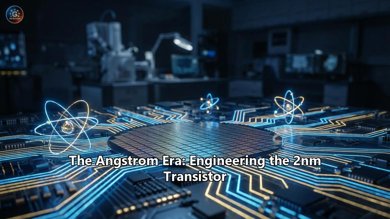
Introduction: The Death of the Nanometer and the Birth of the Angstrom
For nearly two decades, the semiconductor industry has been defined by a single, relentless metric: the nanometer. From 90nm to 14nm, and down to the cutting-edge 3nm chips powering today’s flagship smartphones and AI accelerators, the "node" has been the North Star of technological progress. It was a shorthand for density, speed, and efficiency—a promise that every two years, our digital world would get twice as fast or half as expensive.
But as we stand on the precipice of 2026, that era is effectively over. We have hit the hard wall of physics. The components of a modern transistor are now measured in handfuls of atoms. The "nanometer" is too blunt a tool to describe the precision required to engineer the future.
Welcome to the Angstrom Era.
The shift to the "2nm" process node—and subsequently to 18A (1.8 angstroms) and 14A—is not merely a continuation of the shrinking game. It represents a fundamental reinvention of how chips are built. It involves discarding the transistor architecture that has served us for fifteen years, flipping the power delivery network upside down, and using light so extreme it is absorbed by almost everything in the known universe.
This article explores the engineering marvels, the physics-defying innovations, and the brutal geopolitical and economic stakes of the race to build the 2nm transistor. This is the story of how humanity is learning to manipulate matter at the scale of a single DNA strand to keep the dream of Moore’s Law alive.
Part I: The Architecture of the Impossible
1. The End of the FinFET
To understand the 2nm breakthrough, we must first understand what it is replacing. Since 2011, the industry has relied on the FinFET (Fin Field-Effect Transistor). Before FinFETs, transistors were planar—flat switches on a silicon wafer. As they shrank, they became "leaky," meaning current flowed even when the switch was off, wasting power and generating heat.
The FinFET solved this by pulling the channel (where current flows) up into a 3D vertical fin, allowing the gate (the switch) to wrap around it on three sides. This "tri-gate" control clamped down on leakage and allowed us to scale down to 3nm.
But at 3nm, the FinFET has run out of gas. The fins have become too tall and too narrow to stand upright without collapsing. More importantly, we can no longer fit enough fins in a given footprint to drive the necessary current for high-performance computing. The geometry has hit a dead end.
2. Enter the Nanosheet (Gate-All-Around)
The solution is the Gate-All-Around (GAA) FET, marketed under various names: RibbonFET by Intel, Nanosheet by TSMC, and MBCFET (Multi-Bridge-Channel FET) by Samsung.
If the FinFET was a fin sticking up from the silicon, the GAA FET is a stack of horizontal sheets "floating" above it. Imagine a stack of paper sheets suspended in the air. The gate material wraps completely around each sheet—top, bottom, left, and right.
Why is this revolutionary?- Ultimate Control: By wrapping the gate around all four sides of the channel, engineers achieve the holy grail of electrostatics: near-perfect control over the flow of current. Leakage is virtually eliminated.
- Tunable Performance: In a FinFET, the width of the transistor was determined by the number of fins (1 fin, 2 fins, etc.), which is a discrete integer. You couldn't have 1.5 fins. With Nanosheets, engineers can vary the width of the sheets continuously. A wider sheet equals more drive current (performance); a narrower sheet equals lower power. This allows chip designers to mix and match high-power and high-efficiency transistors with unprecedented granularity.
3. The Manufacturing Nightmare
Building a GAA transistor is akin to constructing a suspension bridge at the atomic scale. The process involves:
- Superlattice Epitaxy: Alternating layers of Silicon (Si) and Silicon-Germanium (SiGe) are grown on the wafer.
- Inner Spacer Formation: A critical step where small pockets are etched into the SiGe layers to create insulation between the gate and source/drain.
- Channel Release: The "magic" step. A selective chemical etch must remove the SiGe layers completely to release the silicon nanosheets, without damaging the silicon itself. The gap between these sheets is often less than 10 nanometers.
- High-K Metal Gate Deposition: The gate dielectric and metal must be deposited into these tiny gaps, wrapping perfectly around each sheet without leaving any air voids. This requires Atomic Layer Deposition (ALD), where materials are laid down one atomic layer at a time.
Part II: Flipping the Script – Backside Power Delivery
While the transistor architecture is getting a makeover, an equally radical change is happening to the wiring. For 60 years, chips have been built like a pizza: the "dough" (transistors) goes on the bottom, and the "toppings" (layers of wiring for signal and power) are stacked on top.
In modern chips, power and data signals fight for space in the same complex web of interconnects (the Back End of Line, or BEOL). Power has to travel through 15-20 layers of increasingly thin wires to reach the transistors at the bottom. This causes two major problems:
- IR Drop: As wires get thinner, resistance increases. By the time power reaches the transistor, a significant voltage has been lost to heat.
- Signal Interference: High-power lines create noise that interferes with delicate data signals nearby.
The Solution: PowerVia and Super Power Rail
The Angstrom Era introduces Backside Power Delivery Network (BSPDN).
The concept is simple but difficult to execute: Separate the power from the data.
- Data wires remain on the front of the wafer.
- Power wires are moved to the back of the wafer.
- Transistors are built as usual.
- Signal wires are built on top.
- The wafer is flipped over.
- The silicon substrate is ground down until it is vanishingly thin (microns thick).
- Nano-Through Silicon Vias (nTSVs) are drilled directly into the back of the wafer to connect power lines straight to the source and drain of the transistors.
- Efficiency: Power paths are shorter and wider (lower resistance), virtually eliminating IR drop.
- Density: Removing power lines from the front side frees up 20-30% of the routing space for data signals, allowing logic cells to be packed tighter. Intel calls their version PowerVia, while TSMC’s version is Super Power Rail.
The biggest risk is thermal management. The silicon substrate used to act as a heat sink. Grinding it away means heat is trapped closer to the transistors. Engineers are developing exotic cooling solutions and thermal interface materials to prevent these dense, powered-from-behind chips from melting.
Part III: Painting with Light – High-NA EUV
To print features at the 2nm node, the industry is transitioning to High-Numerical Aperture (High-NA) Extreme Ultraviolet (EUV) lithography.
Standard EUV machines (0.33 NA) use 13.5nm wavelength light to draw patterns. But at 2nm, the features are so small that 0.33 NA EUV requires "double patterning" (drawing the image twice to get sharper lines), which is slow and expensive.
ASML’s High-NA (0.55 NA) EXE:5000 series machines are the size of a double-decker bus and cost nearly $400 million each. They use larger mirrors to capture light at wider angles, increasing the resolution limit (Rayleigh criterion).The Stochastic Problem
The move to High-NA EUV brings a quantum mechanical headache: Stochastics.
At these scales, light behaves less like a continuous wave and more like a rain of photon particles.
- Photon Shot Noise: If a feature is too small, it might not receive enough photons to define it clearly. It’s like trying to paint a fine line with a spray can; if you don't spray enough dots, the line looks jagged (Line Edge Roughness) or has gaps (Microbridges).
- Defectivity: A single stochastic defect—a gap in a wire or a merged contact—can kill a chip worth thousands of dollars.
To combat this, the industry is moving to massive data analytics, using AI to predict where stochastic defects are likely to occur and adjusting the design (Optical Proximity Correction) to compensate.
Part IV: The Material World – Ruthenium and Beyond
Silicon has been the king of semiconductors, but at the Angstrom scale, copper—the king of interconnects—is being dethroned.
The Copper Problem:In wide wires, copper is an excellent conductor. But as wires shrink below 20nm, the "mean free path" of electrons (the distance an electron travels before hitting an atom) becomes larger than the wire itself. Electrons start bouncing off the walls (grain boundary scattering), and resistance skyrockets. Additionally, copper requires a "barrier layer" (usually Tantalum Nitride) to prevent it from diffusing into silicon. This barrier takes up precious space but conducts no electricity.
The Ruthenium Revolution:Enter Ruthenium (Ru).
- Barrier-less: Ruthenium is chemically stable and doesn't need a thick barrier layer.
- Better Scaling: Even though bulk Ruthenium is less conductive than bulk Copper, at angstrom scales, it wins because you can make the wire entirely out of conductive metal without the "dead space" of a barrier.
- Subtractive Patterning: Intel has pioneered a "subtractive" process for Ruthenium, etching it away to form wires (like a sculpture) rather than filling trenches (like casting). This allows for Airgaps—literally leaving empty space between wires to reduce capacitance and speed up signal transmission.
Part V: The Players and the Roadmap
1. Intel (The Comeback Kid?)
- Node: Intel 18A (1.8 Angstrom class).
- Strategy: Intel is betting the company on beating TSMC to market with the combination of RibbonFET and PowerVia. They plan to reach manufacturing readiness in late 2024/early 2025.
- Key Advantage: They are integrating Backside Power first. If PowerVia works as advertised, Intel could have a significant efficiency lead in 2025.
2. TSMC (The King on the Throne)
- Node: N2 (2nm class).
- Strategy: TSMC is taking a more conservative approach. Their initial N2 node (2025) will introduce Nanosheets but stick with front-side power. They will introduce Backside Power later in the N2P or A16 nodes (2026/2027).
- Key Advantage: Yield and trust. TSMC rarely misses a deadline. By decoupling the two major risks (new transistor + new power delivery), they ensure a smoother ramp for customers like Apple and NVIDIA.
3. Samsung (The Aggressive Challenger)
- Node: SF2 (2nm class).
- Strategy: Samsung was actually the first to mass-produce GAA transistors (MBCFET) at their 3nm node. They have more experience with the architecture than anyone else.
- Key Advantage: First-mover experience on GAA. However, they have struggled with yield and power efficiency compared to TSMC's FinFETs. SF2 is their chance to prove their GAA maturity.
Part VI: Beyond the Chip – Advanced Packaging
In the Angstrom Era, the "System on Chip" (SoC) is dying. It is being replaced by the System of Chips.
You cannot yield a massive 2nm AI processor economically; the defect rate is too high. Instead, companies are breaking chips into "chiplets"—smaller, specialized dies—and stitching them together.
- CoWoS (Chip-on-Wafer-on-Substrate): TSMC’s 2.5D packaging technology that sits at the heart of the AI revolution (powering NVIDIA’s H100/Blackwell). It places memory (HBM) and logic side-by-side on a silicon interposer.
- Hybrid Bonding: The future of 3D stacking. Instead of using solder bumps to connect stacked chips, hybrid bonding fuses the copper pads of two chips directly together (Copper-to-Copper). This allows for connection densities 1,000x higher than standard bumps. This is essential for stacking cache memory directly on top of CPUs (like AMD’s X3D technology) or stacking logic on logic in the future.
Conclusion: The Angstrom Future
The transition to the 2nm node and the Angstrom Era is an inflection point in human history. It is the moment where we stop fighting against quantum mechanics and start engineering with it.
The challenges are immense. The cost of a single wafer is approaching $30,000. The fabs cost $25 billion to build. The energy required to run the EUV lasers is staggering. Yet, the reward is the continuation of the digital revolution: AI models that can reason, smartphones that last for days, and simulations that can model climate change or protein folding with perfect accuracy.
As we look beyond 2nm, towards CFETs (Complementary FETs, where n-type and p-type transistors are stacked on top of each other) and 2D material channels (using Tungsten Disulfide instead of Silicon), one thing is clear: The end of Moore’s Law has been predicted for decades, but the engineers of the Angstrom Era simply refuse to let it die. They are rewriting the rules of physics, one atom at a time.
Reference:
- https://marklapedus.substack.com/p/scaling-copper-interconnects-to-2nm
- https://www.viksnewsletter.com/p/is-ruthenium-the-next-step-in-interconnects
- https://ieeexplore.ieee.org/iel8/16/11049905/11008919.pdf
- https://english.cw.com.tw/article/article.action?id=3921
- https://future-bridge.us/the-high-na-euv-moat-is-this-the-end-of-the-level-playing-field/
- https://www.eenewseurope.com/en/ruthenium-shows-way-to-2nm/