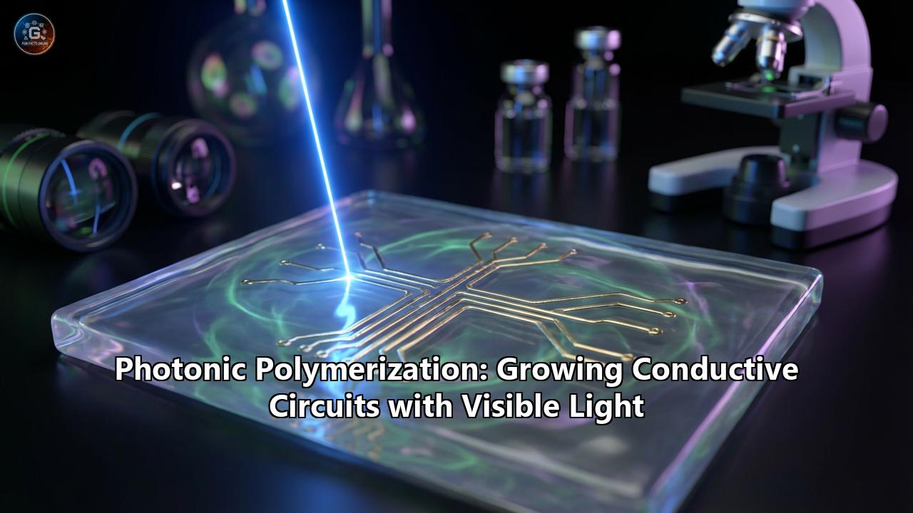
In the shadowy borderlands between materials science and sci-fi, a quiet revolution is taking place. For decades, the creation of electronic circuits has been a violent, industrial affair: etching copper with harsh acids, baking silicon at volcanic temperatures, and soldering metals with lead and tin. It is a process of subtraction—carving pathways out of solid blocks—or forceful addition, melting metal to bind it to plastic. But what if electronics could be grown? What if, instead of soldering a wire, you could simply shine a beam of light into a liquid, and watch a conductive pathway sprout and weave its way toward a connection point, like a vine seeking the sun?
This is the promise of Photonic Polymerization, a cutting-edge field where visible light is used not just to harden plastic, but to synthesize and grow conductive polymer chains in real-time. It is a technology that blurs the line between biology and engineering, allowing us to "write" electricity into soft, living, or flexible matter without heat, vacuum chambers, or toxic solvents.
As we stand in 2025, recent breakthroughs have propelled this concept from niche laboratory curiosity to a scalable manufacturing method. We are no longer just 3D printing plastic shapes; we are optically cultivating the nervous systems of the next generation of robots, wearables, and bio-integrated devices.
Part 1: The Death of the Circuit Board
1.1 The Limitations of "Hard" Electronics
To understand why photonic polymerization is revolutionary, we must first appreciate the tyranny of the printed circuit board (PCB). The PCB is rigid, planar, and brittle. It requires a substrate (usually fiberglass-epoxy) that dictates the form factor of the device. If you want a flexible phone, you have to engineer complex hinges or use expensive flexible PCBs that are prone to fatigue failure.
Furthermore, traditional manufacturing is subtractive and wasteful. Photolithography—the process used to make chips and fine circuits—involves coating a surface with copper, masking it, and then chemically dissolving 90% of the copper. It is an environmentally taxing process.
1.2 The Rise of Organic Conductors
The hero of our story is not copper or gold, but Conductive Polymers. Discovered in the 1970s (earning Heeger, MacDiarmid, and Shirakawa a Nobel Prize in 2000), these are plastics that conduct electricity. Materials like Polyaniline (PANI), Polypyrrole (PPy), and the ubiquitous PEDOT:PSS (poly(3,4-ethylenedioxythiophene) polystyrene sulfonate) combine the mechanical properties of plastic—flexibility, transparency, processability—with the electrical properties of a semiconductor or metal.
For years, the challenge was processing them. You usually had to spray them as an ink or spin-coat them as a thin film. You couldn't easily "build" a 3D wire out of them in mid-air or inside a biological tissue. That is, until we learned how to make them react to light.
Part 2: The Science of Photonic Polymerization
2.1 How Light Becomes Matter
Photonic polymerization differs fundamentally from standard UV-curing used in dental fillings or SLA 3D printers. In standard UV curing, light hits a photoinitiator, creating a radical that freezes a liquid resin into a solid plastic. The plastic is an insulator.
In Photonic Polymerization for Conductivity, the goal is to use light to polymerize a specific monomer (like EDOT) into a long, conjugated chain that allows electrons to flow. This is chemically complex because the oxidation potential required to turn EDOT into conductive PEDOT is high.
The Mechanism: Oxidative Photopolymerization
The magic usually happens via a mechanism called Photogenerated Acid (PGA) or Photoredox Catalysis.
- The Bath: You start with a liquid solution containing the monomer (e.g., EDOT) and a photosensitizer (a molecule that absorbs light).
- The Trigger: When a specific wavelength of visible light (say, a green laser at 532nm or a blue LED at 405nm) hits the photosensitizer, it enters an excited state.
- The Electron Heist: This excited molecule steals an electron from an oxidant or directly transfers energy to an initiator, creating a reactive radical.
- Chain Growth: These radicals attack the EDOT monomers, linking them together. As they link, they expel protons and form a conjugated backbone—a highway for electrons.
- Doping in Real-Time: Crucially, the process must also "dope" the polymer (introduce charge carriers). Often, the byproducts of the reaction act as dopants, locking the polymer into a conductive state instantly.
2.2 The Breakthrough: Initiator-Free Systems (2024-2025)
One of the most significant recent hurdles was the "initiator problem." Traditional photoinitiators are often toxic or require UV light, which damages biological cells and degrades organic materials.
In late 2024 and 2025, researchers unveiled initiator-free visible-light polymerization. By tuning the chemical structure of the monomers themselves to be slightly photo-active, or using biocompatible dyes like Riboflavin (Vitamin B2) as a helper, scientists can now grow conductive wires using soft, safe visible light.
- Self-Catalysis: A groundbreaking study revealed that PEDOT:PSS itself can act as a catalyst. As the wire grows, the growing tip catalyzes the reaction for the next monomer, meaning the light just needs to guide the growth rather than force every single chemical bond. This allows for "living" wires that extend outward from a light source.
Part 3: The Toolkit – Lasers, Projectors, and Holograms
How do you shape a liquid into a wire? The method of light delivery determines the structure.
3.1 Laser Direct Writing (LDW)
Imagine a pen that writes with light. A focused laser beam moves through a bath of monomer solution. Wherever the focal point touches, the liquid turns into a solid conductive wire. This technique, known as Multiphoton Lithography or Two-Photon Polymerization (2PP), allows for sub-micron precision.
- Application: Creating invisible, microscopic wiring on the surface of a contact lens or connecting individual neurons in a petri dish.
3.2 Digital Light Processing (DLP)
Instead of a single point, DLP uses a projector chip (DMD) to flash an entire image of a circuit layer at once.
- The "Vat" Method: A build plate dips into the conductive resin. The projector flashes the image of the circuit traces. The layer solidifies. The plate lifts, and the next layer is flashed.
- Advantage: Speed. You can print a complex, multi-layer circuit board in minutes.
- The Challenge: Most conductive polymers are dark blue or black. They absorb light greedily, preventing the light from curing deep layers. Recent innovations in "bleaching" photoinitiators (which become transparent after reacting) have solved this, allowing for thicker, more robust circuits.
3.3 Holographic Lithography
The frontier of the field. By using interference patterns of light (holograms), scientists can cure an entire 3D volume simultaneously. Imagine a tank of liquid monomer; suddenly, a flash of light occurs, and a fully formed 3D conductive lattice appears floating in the center. This effectively "teleports" a circuit into existence within a second.
Part 4: Materials of the Future
The ink is just as important as the pen.
4.1 PEDOT: The Workhorse
PEDOT:PSS is the standard. It’s stable, transparent, and highly conductive. When polymerized with light, it forms a hydrogel-like structure—soft, wet, and conductive.
- Conductivity: Recent light-cured PEDOT films have reached conductivities of over 2,000 S/cm, rivaling Indium Tin Oxide (ITO) and approaching some metals.
4.2 Metallic Polyaniline (2D PANI)
A massive breakthrough in early 2025 described a "2D Polyaniline Crystal" that conducts electricity like a metal. Unlike standard polymers where electrons hop clumsily between chains, this new structure allows electrons to flow essentially unimpeded in all directions. Integrating this material with photonic growth is the current "Holy Grail," potentially allowing us to print wires as conductive as copper but as flexible as nylon.
4.3 Bio-Hybrid Inks
Researchers are now mixing conductive monomers with biological hydrogels (like gelatin or alginate). The result is a "bionic jelly"—a material that can support living cells while conducting electrical signals. This is the foundation of the new field of Bio-integrated Electronics.
Part 5: Applications – From Cyborg Plants to Brain Interfaces
This is where the rubber meets the road (or rather, where the light meets the liquid).
5.1 In Vivo "Wiring" of Biology
Perhaps the most startling application is growing circuits inside living tissue.
- The Xenobot Link: In experiments involving model organisms (like hydra or even mouse skin), researchers injected a monomer solution into the tissue. By shining a harmless red or near-infrared light through the skin, they triggered polymerization under the surface.
- Result: A conductive electrode grew in situ, perfectly conforming to the complex, squishy geometry of the biological tissue. This eliminates the need for invasive surgery to implant rigid electrodes. We are moving toward a future where a neural interface is "injected and grown" rather than "cut and implanted."
5.2 Soft Robotics and "Sensory Skin"
Robots made of soft silicone need soft sensors. Traditional wires break when stretched. Photonic polymerization allows engineers to print conductive meandering traces directly onto the surface of a soft robot hand.
- Self-Healing Circuits: Because the polymerization is chemical, some of these systems are self-healing. If a wire breaks, you can inject a drop of monomer and shine a light on the break to "regrow" the connection.
5.3 4D Printing (Time-Evolving Circuits)
4D printing adds the dimension of time—objects that change shape. By patterning conductive polymer heaters into a shape-memory polymer, engineers can create flat sheets that, when activated by a current, fold themselves into complex origami robots. Photonic polymerization allows these heating elements to be patterned with extreme precision, controlling the folding sequence perfectly.
5.4 Smart Plants
In a vivid display of "Solarpunk" technology, scientists have used this method to print circuits on the leaves of living plants without harming them.
- The Idea: Turn a leaf into a sensor that detects environmental pollutants or drought stress and transmits the data via the printed antenna.
- The Method: A gel containing the monomer is brushed onto the leaf. A projector maps the veins of the leaf and projects a circuit pattern that avoids blocking the stomata (breathing pores). The light cures the circuit instantly.
Part 6: Challenges and The "Dark" Cure
Despite the excitement, significant hurdles remain.
6.1 The Oxygen Inhibition Problem
Oxygen is the enemy of radical polymerization. It scavenges the radicals before they can build the chain. Traditionally, this meant printing had to happen in an inert nitrogen chamber—expensive and impractical for "growing wires on a patient's skin."
- The Solution: The "Polymerizing Through Oxygen" mechanism. New additive-free systems consume oxygen faster than it can diffuse in, creating a localized oxygen-free zone where the wire can grow.
6.2 Resolution vs. Conductivity Trade-off
Generally, to get higher resolution (finer wires), you need faster polymerization. But faster polymerization often leads to shorter, more chaotic polymer chains, which conduct electricity poorly. Slow growth yields long, ordered, highly conductive chains but takes... well, too long. Finding the "Goldilocks" zone of light intensity is an active area of AI-driven materials research.
6.3 Cytotoxicity of Monomers
While the light is safe, the unpolymerized monomers (like pure pyrrole or EDOT) can be toxic to cells. The reaction must be 100% efficient, leaving no toxic residue, or the precursors must be encapsulated in safe carriers until the light hits them.
Part 7: The Future – The "Photosynthetic" Computer
Looking forward, the convergence of photonics and polymerization suggests a radical shift in manufacturing.
7.1 The Desktop Fab
Imagine a desktop device that looks like a fish tank. You place a damaged smartphone or a blank piece of plastic inside. Lasers scan the object, identify the geometry, and "grow" a new antenna, a battery connector, or a touch sensor directly onto it. No waste, no soldering fumes.
7.2 Neuromorphic Computing Hardware
The brain grows connections (synapses) based on activity. Photonic polymerization allows us to mimic this hardware. We could build "optical neural networks" where connections are strengthened (polymerized thicker) or weakened (photodegraded) by light pulses, creating a physical computer that learns by physically rewiring itself.
7.3 Space Manufacturing
On deep space missions, carrying spare parts is heavy. Carrying a liter of "universal conductive resin" is light. Astronauts could use sunlight—concentrated by lenses—to polymerize spare circuit boards, sensor arrays, or solar cell interconnects on demand.
Conclusion
Photonic Polymerization is more than just a new way to make wires. It is a fundamental shift in our relationship with materials. It represents a move away from the "heat and beat" metallurgy of the Iron Age and the toxic lithography of the Silicon Age, toward an era of soft, grown, and light-sculpted electronics.As we master the ability to grow conductive pathways with the precision of a laser and the gentleness of a sunbeam, we unlock a future where our technology is as organic, adaptable, and seamless as nature itself. The circuit board of the future won't be a green rectangle inside a black box; it will be a transparent, flexible web grown directly on, in, or around the things that matter most.
Reference:
- https://ouci.dntb.gov.ua/en/works/7qYrBLb7/
- https://pmc.ncbi.nlm.nih.gov/articles/PMC12021782/
- https://patents.google.com/patent/US5545308A/en
- https://www.mdpi.com/2073-4352/12/8/1109
- https://pubs.acs.org/doi/10.1021/acsomega.5c08520
- http://www.diva-portal.org/smash/get/diva2:1163572/FULLTEXT01.pdf
- https://www.youtube.com/watch?v=V86t5td1gVg
- https://www.mdpi.com/2076-3417/15/7/4028
- https://en.wikipedia.org/wiki/Conductive_polymer