For decades, the foundation of our modern technological world has been built on a single, fundamental particle: the electron. Through the microscopic circuitry of silicon chips, the controlled flow of electrons has given us everything from the personal computer to the smartphone, from the early internet to the dawn of artificial intelligence. But we are rapidly approaching a physical and thermal wall. As we pack billions of transistors into spaces no larger than a fingernail, electrons face resistance, generating massive amounts of heat and consuming astronomical levels of energy. The era of Moore’s Law—the historical trend of computing power doubling every two years—is slowing down under the weight of its own thermal limitations.
To push the boundaries of what is possible, science is turning to a faster, more elegant, and infinitely more efficient messenger: the photon.
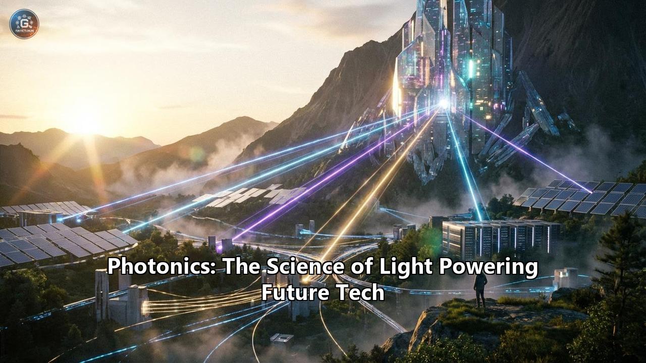
Welcome to the era of photonics. This is the science of generating, controlling, and detecting light to process and transmit information. By replacing the flow of electricity with the flow of light, we are fundamentally rewriting the physical rules of computing, telecommunications, healthcare, and global infrastructure. In a world hungering for massive computational power to feed artificial intelligence and quantum systems, photonics stands as the ultimate paradigm shift—a transition from the electronic age to the light age.
This comprehensive exploration will dive deep into the mechanics of photonics, its revolutionary impact on current and future technologies, and how the mastery of light is quite literally illuminating the path forward for human progress.
1. The Physics of Light: Why Photons Beat Electrons
To understand why photonics is the future, we must look at the fundamental differences between photons and electrons.
Electrons have mass and interact strongly with one another. When they travel through copper wires or silicon tracks, they experience electrical resistance. This resistance results in energy loss, primarily in the form of heat. In a modern data center, managing this heat requires massive cooling infrastructure, which often consumes nearly as much electricity as the processors themselves.
Photons, on the other hand, are massless particles of light. They do not carry an electrical charge, meaning they do not interact with one another in the same way electrons do. You can cross two beams of light, and they will pass right through each other without interference. Furthermore, photons travel at the absolute speed limit of the universe: the speed of light.
When applied to computing and data transmission, these physical properties offer distinct advantages:
- Unprecedented Speed: Light can transmit data across vast distances with near-zero latency.
- Massive Bandwidth: Through a technique called wavelength-division multiplexing (WDM), multiple streams of data can be transmitted simultaneously over the same channel simply by using different colors (wavelengths) of light.
- Extreme Energy Efficiency: Because photons do not suffer from the same resistance as electrons, photonic systems generate virtually no heat during data transmission, drastically reducing the energy required for cooling and power.
2. The Core Building Blocks of the Photonic Ecosystem
Just as traditional electronics rely on capacitors, resistors, and transistors, the field of photonics relies on its own set of microscopic components, integrated onto what are known as Photonic Integrated Circuits (PICs).
Lasers and Light SourcesEverything begins with the generation of light. While early photonic systems relied on bulky external lasers, modern silicon photonics integrates microscopic laser arrays directly onto the chip. Innovations such as frequency-comb-based sources allow a single laser to generate multiple precisely spaced wavelengths, each capable of carrying an independent data stream.
WaveguidesIf lasers are the power plants, waveguides are the transmission lines. Usually made of silicon or silicon nitride, waveguides act as microscopic tunnels that trap and guide light across the chip. Because of the high refractive index of silicon, light bounces off the internal walls of the waveguide, traveling exactly where it is needed without leaking out.
ModulatorsA constant beam of light carries no information. To transmit data, the light must be modulated—turned on and off, or altered in phase and intensity, to represent digital 1s and 0s. Advances in microring modulators have allowed researchers to manipulate light with stunning efficiency. Recently, devices as small as a strand of hair have demonstrated the ability to transmit data at a blistering 1,000 gigabits per second while consuming a mere 4 joules of energy.
PhotodetectorsAt the receiving end of a photonic circuit, light must be translated back into a language that traditional electronic systems can understand. Photodetectors absorb the incoming photons and convert them back into electrical signals.
Interferometers and Beam SplittersComponents like Mach-Zehnder interferometers (MZIs) split a beam of light, alter the phase of one half, and recombine them. This creates constructive or destructive interference, a property that is increasingly being used not just to route light, but to perform complex mathematical calculations purely through optics.
3. Artificial Intelligence: The Photonic Rescue Mission
No sector is driving the commercialization of photonics faster than Artificial Intelligence. The rapid rise of Large Language Models (LLMs), generative AI, and deep learning has created an insatiable hunger for computational power.
We are currently facing an AI energy crisis. Estimates suggest that by 2030, data center power demand could surge by 160%, reaching 945 terawatt-hours annually—an amount equivalent to the entire electricity consumption of countries like Japan. Today’s AI training facilities house hundreds of thousands of specialized silicon chips, each drawing immense amounts of power and generating blistering heat. If AI continues scaling on traditional silicon electronics, the energy requirements will soon outpace the capacity of our global power grids.
This is where Photonic AI Chips enter the stage. By transitioning from pure electronic computation to optical interconnected architectures, we can bypass the copper bottlenecks that throttle current AI systems.
In-Memory Compute and Optical InterconnectsIn a traditional computing architecture, a significant amount of time and energy is wasted simply shuttling data back and forth between the processor and the memory (the "von Neumann bottleneck"). Photonic chips utilize optical interconnects—using light to bridge the gap between memory and processing units. Co-packaged optics (CPO) bring the optical connections directly into the processor package, allowing data to flow at terabits per second with minimal energy loss. Implementing optical interconnects in data centers can reduce energy consumption by up to 50% and increase data transfer rates by 30%.
Photonic Neural Networks and Native Processing UnitsBeyond just moving data, light is now being used to compute data. Companies are deploying commercial photonic processors, sometimes referred to as Native Processing Units (NPUs) or neuromorphic processors. These chips emulate the human brain's neural networks, performing complex matrix multiplications—the foundational math of AI deep learning—at the speed of light. Because light can naturally perform multiple operations simultaneously (analog parallel processing) without generating heat, these photonic AI accelerators can reduce the power consumption of deep learning workloads by up to 90%.
By moving AI processing into the optical domain, we ensure that the future of artificial intelligence is not only exponentially faster but environmentally sustainable.
4. Quantum Photonics: Engineering the Impossible
If standard photonics represents a leap in computing and communication, quantum photonics represents an entirely new dimension of physics. While classical computers process information in bits (representing exactly 0 or 1), quantum computers use quantum bits, or qubits, which can exist in a superposition of both 0 and 1 simultaneously.
Photonics has emerged as the most promising platform for unlocking the true potential of quantum technologies.
Optical Quantum ComputingMany early quantum computers rely on superconducting qubits or ion traps, which must be kept in massive, multi-million-dollar cryogenic refrigeration systems operating at temperatures colder than deep space. Photonic quantum computers, however, offer a groundbreaking alternative: they can largely operate at room temperature.
Using single photons as qubits, companies like QuiX Quantum, Xanadu, and ORCA Computing are building quantum processors that guide individual particles of light through complex networks of optical channels. Because photons naturally do not interact with the environment, they maintain their fragile quantum states (coherence) much better than other types of qubits. Furthermore, because photonic quantum chips can be interconnected using standard fiber-optic cables, scaling up to massive, distributed quantum supercomputers is vastly more feasible. These optical quantum computers will soon be capable of simulating complex molecular structures in seconds, revolutionizing drug discovery, materials science, and battery development.
The Unhackable Internet: Quantum Key Distribution (QKD)With the impending rise of quantum computers comes a terrifying security threat: the ability to crack the encryption that currently protects all global digital communications, banking systems, and government secrets. The solution lies in the very technology that creates the threat.
Quantum Key Distribution (QKD) is a secure communication method driven by quantum photonics. It involves encoding cryptographic keys into individual photons. According to the laws of quantum mechanics (specifically Heisenberg's Uncertainty Principle), merely observing or measuring a quantum system alters its state. Therefore, if a hacker attempts to intercept a photon carrying a quantum key, the photon's state immediately changes, alerting the sender and receiver to the breach.
This technology is not science fiction; it is a reality today. Researchers have already developed Quantum Random Number Generators (QRNGs) and integrated transmitter/receiver chips that make QKD scalable, paving the way for a mathematically unhackable "Quantum Internet".
Quantum Sensors and GravimetryBeyond computing and networking, quantum photonics is redefining how we measure the physical world. Quantum sensors exploit the extreme sensitivity of quantum states to detect minute changes in gravity, magnetic fields, and time. In navigation, quantum gravimeters and accelerometers can provide ultra-precise positioning data without relying on GPS satellites, making them invaluable for deep-sea exploration, space travel, and autonomous systems operating in signal-denied environments.
5. Telecommunications and the 6G Horizon
The internet as we know it is already a largely photonic construct. Global data travels through millions of miles of undersea fiber-optic cables. However, the "last mile" of data delivery and the internal routing within data centers have remained largely electronic.
As we look toward the deployment of 6G networks and the expansion of edge computing, the sheer volume of data being generated requires a fully integrated photonic infrastructure. Integrated photonics allows for ultra-high-frequency signal processing in the gigahertz and terahertz ranges. This translates to wireless and wired networks capable of handling augmented reality (AR) metaverses, real-time remote robotic surgery, and vast arrays of Internet of Things (IoT) devices without dropping a single packet of data.
Furthermore, photonics is taking communication to the stars. In satellite networks and space exploration, size, weight, and power (SWaP) are critical constraints. Photonic communication systems replace heavy copper wiring and bulky radio frequency antennas with lightweight, highly reliable laser communication terminals. This allows satellites to transmit massive amounts of high-resolution Earth-observation data back to the ground more efficiently.
6. Sensing the World: Lidar and Autonomous Machines
The dream of fully autonomous vehicles relies heavily on the machine's ability to perceive its surroundings with flawless accuracy in real time. Cameras and traditional radar can only do so much. The ultimate solution is LiDAR (Light Detection and Ranging).
LiDAR systems emit rapid pulses of laser light—millions per second—bouncing them off surrounding objects and measuring the time it takes for the light to return. This creates a hyper-accurate, 3D point-cloud map of the environment. Historically, LiDAR units were bulky, mechanical, spinning cylinders mounted on the roofs of cars, costing tens of thousands of dollars.
Thanks to advancements in Photonic Integrated Circuits, solid-state LiDAR has been miniaturized onto single chips. By using optical phased arrays (OPAs) to steer laser beams electronically without any moving parts, photonic LiDAR is now compact, robust, and inexpensive enough to be integrated invisibly into the bumpers and headlights of consumer vehicles, or the chassis of delivery drones. This miniaturization is the key to unlocking safe, mass-market autonomous mobility.
7. Biophotonics: Illuminating the Human Body
The intersection of photonics and biology—biophotonics—is transforming medical diagnostics and treatment. Light is non-invasive, fast, and capable of interacting with biological tissues at the molecular level.
Advanced Imaging and DiagnosticsBreakthroughs in optical coherence tomography (OCT) and multi-photon microscopy allow doctors to capture high-resolution, 3D images of tissue structures beneath the skin without the need for surgical biopsies. Photonic sensors can detect biomarkers for diseases like cancer or viral infections in blood or saliva with unprecedented speed and accuracy.
Surface-Enhanced Raman Spectroscopy (SERS)One of the most profound breakthroughs in the past decade is the development of photonic-enabled Surface-Enhanced Raman Spectroscopy (SERS). This technique uses light to identify the unique molecular "fingerprints" of substances. By integrating SERS onto portable photonic chips, doctors can perform rapid, point-of-care diagnostics, and security personnel can instantly detect trace amounts of explosives or biological hazards in the environment.
Wearables and In-Vivo SensorsAs photonic chips become smaller and cheaper, they are being integrated into wearable health devices. Future smartwatches will use advanced photonic sensors to non-invasively monitor blood glucose levels, oxygen saturation, and hydration by safely shining specific wavelengths of light through the skin and analyzing the reflected spectra.
8. Precision Manufacturing and Ultrafast Lasers
The physical things we interact with daily are increasingly being shaped by light. The manufacturing sector has been revolutionized by the deployment of ultrafast lasers—such as femtosecond lasers, which emit pulses of light lasting just quadrillionths of a second.
These ultrafast pulses deliver massive peak power to a highly targeted area, instantly vaporizing material before heat has a chance to spread to surrounding areas. This "cold ablation" process allows for the ultra-precise cutting of delicate materials like medical stents, smartphone display glass, and even the silicon wafers used to make electronic chips themselves. Without photonics, the modern manufacturing tolerances required to build today's advanced technology would be physically impossible to achieve.
9. The Bottlenecks and Challenges Ahead
While the promise of a photonics-driven future is breathtaking, the industry faces significant hurdles as it transitions from laboratory breakthroughs to massive commercial scale.
The Integration ChallengeThe most difficult engineering hurdle has been integrating active light-emitting components directly onto silicon chips. Silicon is an excellent material for routing light, but it is an incredibly poor material for generating light. Consequently, manufacturers have historically had to use exotic materials like Indium Phosphide or Gallium Arsenide to build lasers, and then meticulously bond them to silicon wafers. Developing seamless, scalable, and high-yield manufacturing processes for these hybrid chips is a top priority for semiconductor giants and specialized foundries.
Packaging and AlignmentIn electronics, connecting a chip to a circuit board requires soldering metal pins. In photonics, connecting a microscopic optical fiber to a waveguide on a chip requires sub-micron precision. If the alignment is off by even a fraction of a hair's width, the light escapes, and the signal is lost. Advanced optical packaging techniques are highly complex and represent a significant portion of the cost of photonic devices.
StandardizationUnlike the electronics industry, which has spent fifty years developing standardized libraries of transistors and universal design rules (PDKs - Process Design Kits), the integrated photonics industry is still in its relative infancy. There is a lack of uniform design and manufacturing standards, making it harder for fabless startups to quickly design and prototype new chips. However, massive investments from global tech alliances and governments are rapidly maturing the ecosystem.
10. The Road Ahead: A Brilliant Future
We are standing on the precipice of the most significant architectural shift in computing since the invention of the transistor. As Moore's Law draws to its inevitable close, the science of light is stepping in to shatter the ceiling of technological progress.
The timeline is accelerating. Technologies that were considered speculative laboratory experiments a decade ago are now being deployed in commercial data centers. Gartner recently included photonic computing in its Hype Cycle for Data Center Infrastructure, signaling its arrival as a core, investable reality. From the development of AI models that process data with zero heat generation, to unhackable quantum networks, to medical sensors that can detect illness from a single drop of blood, photonics is the foundational layer of tomorrow's infrastructure.
The future of information technology, sensing, and global connectivity is no longer written solely in copper and electrons. It is being written in glass, silicon, and the boundless potential of the photon. The age of light is here, and it is illuminating a smarter, faster, and more sustainable future for humanity.
Reference:
- https://www.aishe24.com/2026/01/photonic-chips-usher-in-new-era-for.html
- https://www.photonics.com/Articles/Photonics-Reshapes-the-Future-of-Computing/a69683
- https://lumiaires.ai/f/why-photonic-ai-chips-are-the-next-frontier
- https://www.photonics.com/Articles/Photonic-Hardware-Ascends-in-the-Age-of-AI/a71985
- https://newsroom.lamresearch.com/silicon-photonics-ai-energy-efficiency?blog=true
- https://www.quantum-photonics.de/en/news-detail-page/integrated-photonics-the-future-of-optical-technology.63985
- https://www.technavio.com/report/photonic-chips-for-ai-market-industry-analysis
- https://www.techbriefs.com/component/content/article/54249-doc-9796
- https://www.weforum.org/stories/2025/08/photonic-computing-promise-commercialization/
- https://www.asphericon.com/en/blog/250916-quantum-technology-and-photonics-how-photonics-is-driving-the-quantum-revolution/
- https://eicscalingclub.eu/news/quix-quantum-interview
- https://www.findlight.net/blog/top-photonics-breakthroughs-decade/
- https://picmagazine.net/article/122042/10th_PIC_International_explores_the_future_of_quantum_photonics
- https://ioplus.nl/en/posts/pic-summit-2025-global-photonic-industry-to-scale-for-the-ai-era